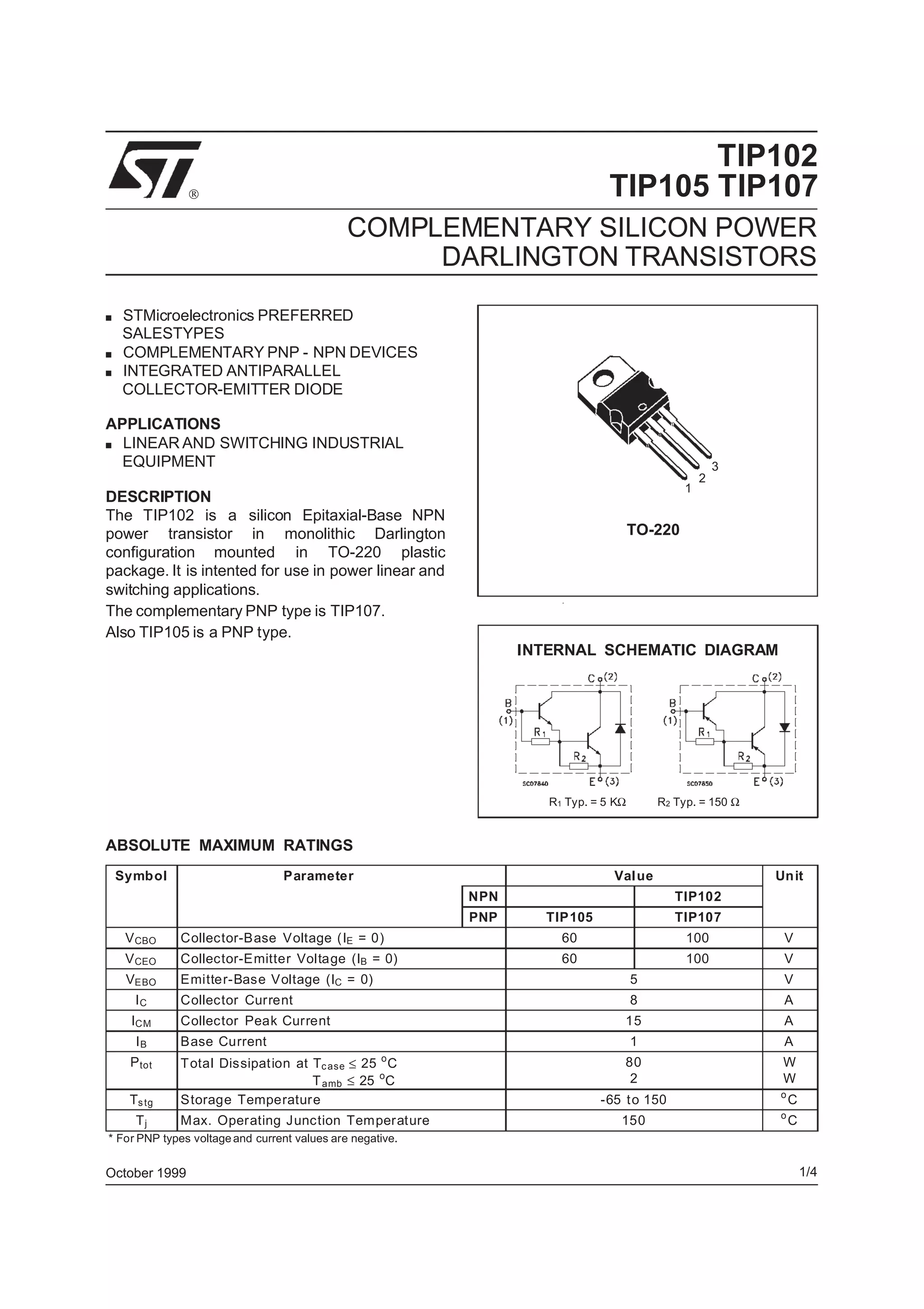
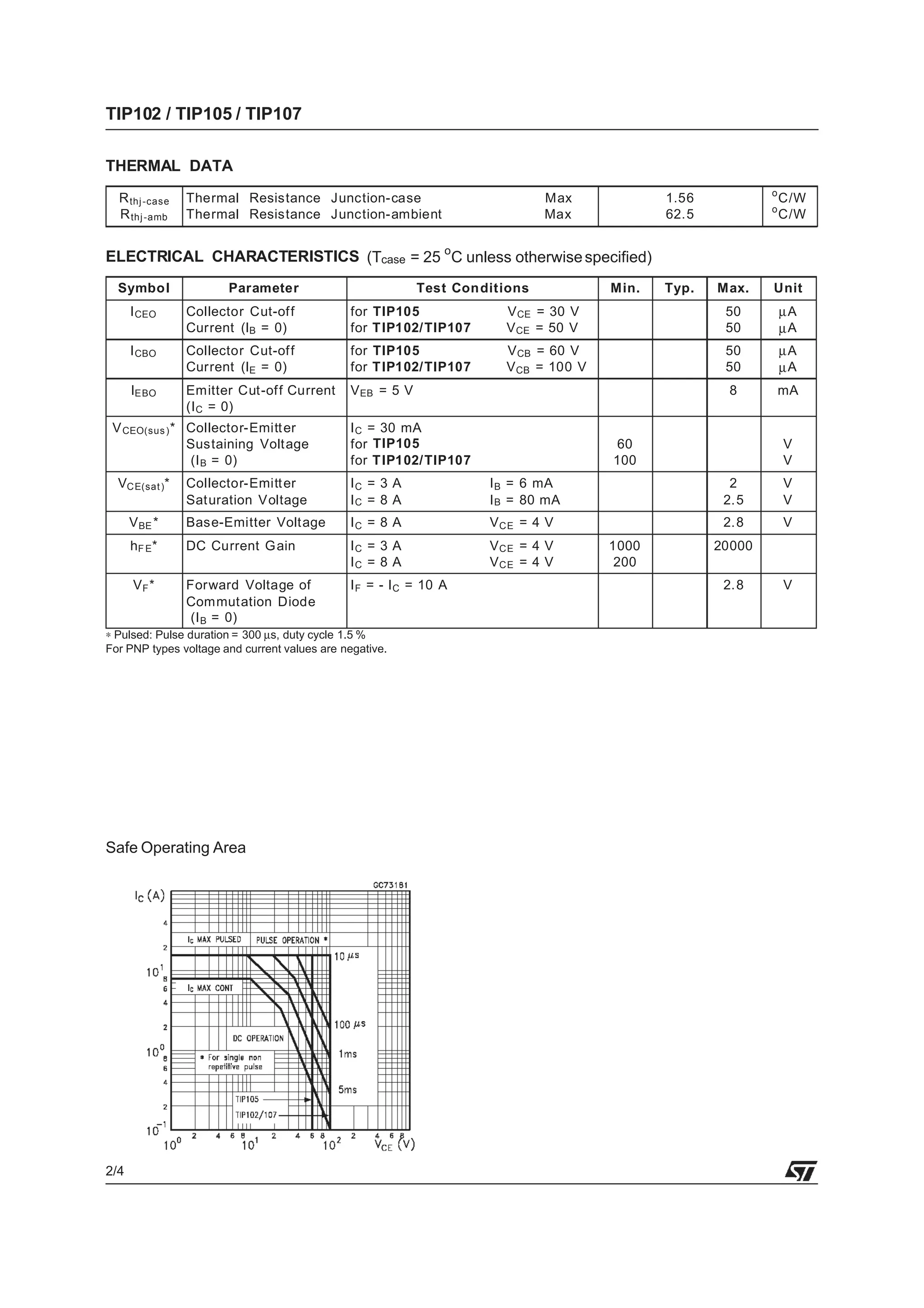
Original PNP Transistor TIP102 TO-220 New STMicroelectronics
1. TIP102
TIP105 TIP107
COMPLEMENTARY SILICON POWER
DARLINGTON TRANSISTORS
s STMicroelectronics PREFERRED
SALESTYPES
s COMPLEMENTARY PNP - NPN DEVICES
s INTEGRATED ANTIPARALLEL
COLLECTOR-EMITTER DIODE
APPLICATIONS
s LINEAR AND SWITCHING INDUSTRIAL
EQUIPMENT
DESCRIPTION
The TIP102 is a silicon Epitaxial-Base NPN
power transistor in monolithic Darlington
configuration mounted in TO-220 plastic
package. It is intented for use in power linear and
switching applications.
The complementary PNP type is TIP107.
Also TIP105 is a PNP type.
®
INTERNAL SCHEMATIC DIAGRAM
October 1999
ABSOLUTE MAXIMUM RATINGS
Symbol Parameter Value Unit
NPN TIP102
PNP TIP105 TIP107
VCBO Collector-Base Voltage (IE = 0) 60 100 V
VCEO Collector-Emitter Voltage (IB = 0) 60 100 V
VEBO Emitter-Base Voltage (IC = 0) 5 V
IC Collector Current 8 A
ICM Collector Peak Current 15 A
IB Base Current 1 A
Ptot Total Dissipation at Tcase ≤ 25 o
C
Tamb ≤ 25 o
C
80
2
W
W
Tstg Storage Temperature -65 to 150 o
C
Tj Max. Operating Junction Temperature 150 o
C
* For PNP types voltageand current values are negative.
1
2
3
TO-220
R1 Typ. = 5 KΩ R2 Typ. = 150 Ω
1/4
2. THERMAL DATA
Rthj-case
Rthj-amb
Thermal Resistance Junction-case Max
Thermal Resistance Junction-ambient Max
1.56
62.5
o
C/W
o
C/W
ELECTRICAL CHARACTERISTICS (Tcase = 25 o
C unless otherwisespecified)
Symbol Parameter Test Conditions Min. Typ. Max. Unit
ICEO Collector Cut-off
Current (IB = 0)
for TIP105 VCE = 30 V
for TIP102/TIP107 VCE = 50 V
50
50
µA
µA
ICBO Collector Cut-off
Current (IE = 0)
for TIP105 VCB = 60 V
for TIP102/TIP107 VCB = 100 V
50
50
µA
µA
IEBO Emitter Cut-off Current
(IC = 0)
VEB = 5 V 8 mA
VCEO(sus)* Collector-Emitter
Sustaining Voltage
(IB = 0)
IC = 30 mA
for TIP105
for TIP102/TIP107
60
100
V
V
VCE(sat)* Collector-Emitter
Saturation Voltage
IC = 3 A IB = 6 mA
IC = 8 A IB = 80 mA
2
2.5
V
V
VBE* Base-Emitter Voltage IC = 8 A VCE = 4 V 2.8 V
hFE* DC Current Gain IC = 3 A VCE = 4 V
IC = 8 A VCE = 4 V
1000
200
20000
VF* Forward Voltage of
Commutation Diode
(IB = 0)
IF = - IC = 10 A 2.8 V
∗ Pulsed: Pulse duration = 300 µs, duty cycle 1.5 %
For PNP types voltage and current values are negative.
Safe Operating Area
TIP102 / TIP105 / TIP107
2/4
3. DIM.
mm inch
MIN. TYP. MAX. MIN. TYP. MAX.
A 4.40 4.60 0.173 0.181
C 1.23 1.32 0.048 0.051
D 2.40 2.72 0.094 0.107
D1 1.27 0.050
E 0.49 0.70 0.019 0.027
F 0.61 0.88 0.024 0.034
F1 1.14 1.70 0.044 0.067
F2 1.14 1.70 0.044 0.067
G 4.95 5.15 0.194 0.203
G1 2.4 2.7 0.094 0.106
H2 10.0 10.40 0.393 0.409
L2 16.4 0.645
L4 13.0 14.0 0.511 0.551
L5 2.65 2.95 0.104 0.116
L6 15.25 15.75 0.600 0.620
L7 6.2 6.6 0.244 0.260
L9 3.5 3.93 0.137 0.154
DIA. 3.75 3.85 0.147 0.151
P011C
TO-220 MECHANICAL DATA
TIP102 / TIP105 / TIP107
3/4