Download to read offline
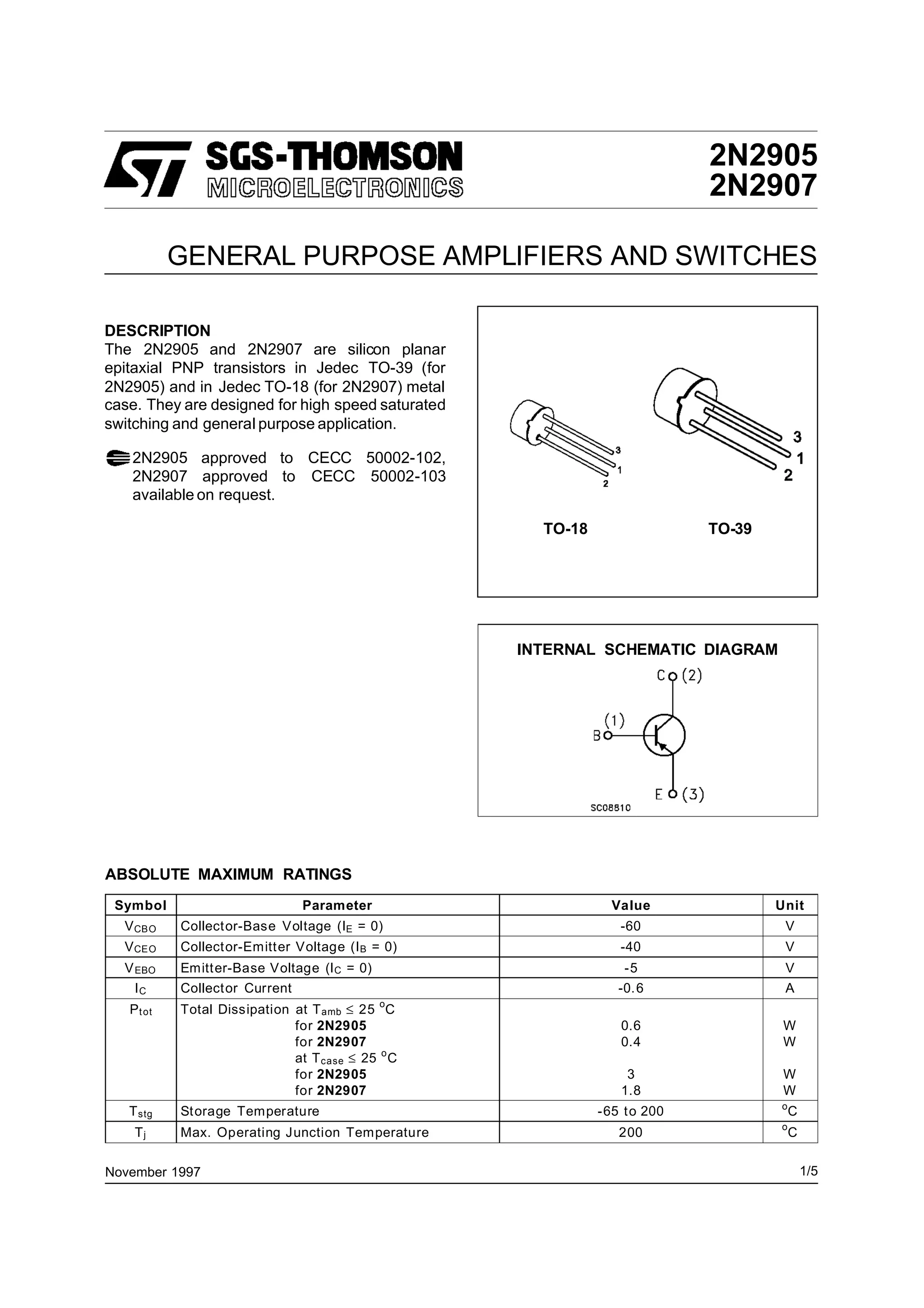
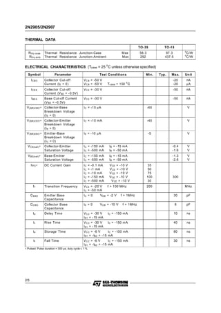
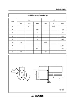
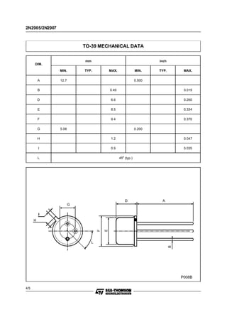

This document provides specifications for the 2N2905 and 2N2907 silicon planar epitaxial PNP transistors. The 2N2905 is housed in a JEDEC TO-39 metal case and the 2N2907 is in a JEDEC TO-18 metal case. Both transistors are designed for high-speed saturated switching and general purpose applications. The document includes maximum ratings, thermal characteristics, electrical characteristics under pulsed test conditions, and mechanical dimension drawings for each package type.