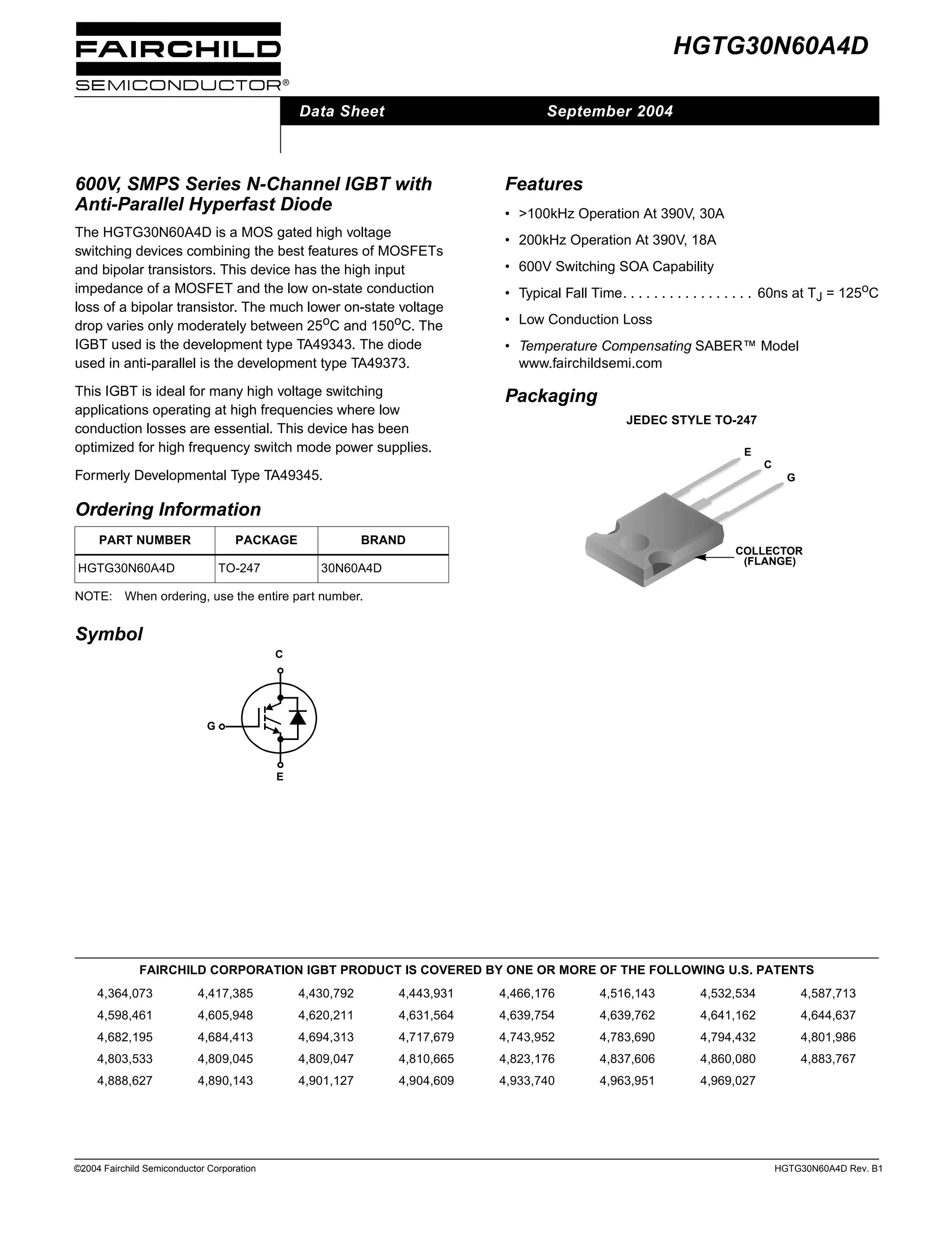
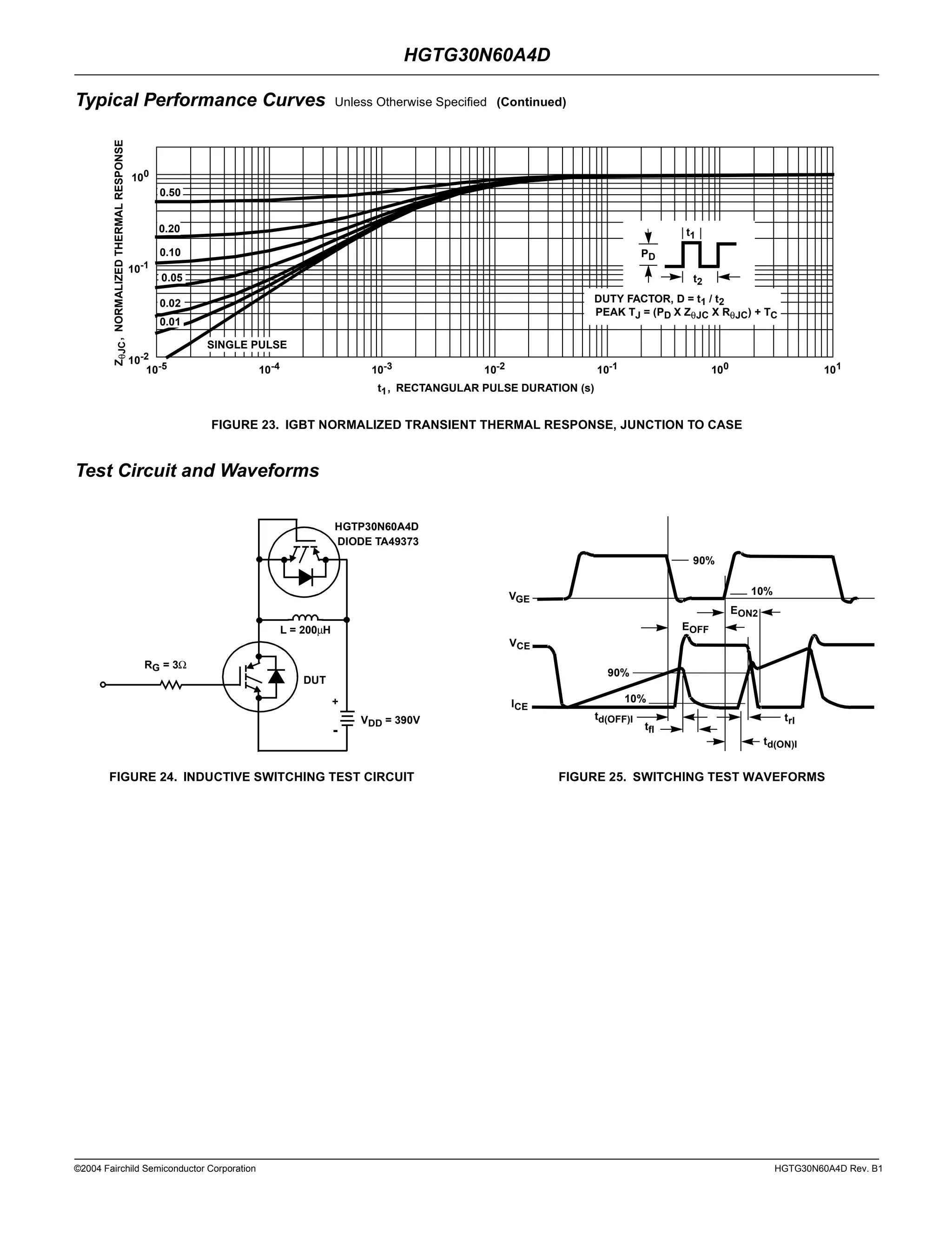
©2004 Fairchild Semiconductor Corporation HGTG30N60A4D Rev. B1
HGTG30N60A4D
600V, SMPS Series N-Channel IGBT with
Anti-Parallel Hyperfast Diode
The HGTG30N60A4D is a MOS gated high voltage
switching devices combining the best features of MOSFETs
and bipolar transistors. This device has the high input
impedance of a MOSFET and the low on-state conduction
loss of a bipolar transistor. The much lower on-state voltage
drop varies only moderately between 25oC and 150oC. The
IGBT used is the development type TA49343. The diode
used in anti-parallel is the development type TA49373.
This IGBT is ideal for many high voltage switching
applications operating at high frequencies where low
conduction losses are essential. This device has been
optimized for high frequency switch mode power supplies.
Formerly Developmental Type TA49345.
Symbol
Features
• >100kHz Operation At 390V, 30A
• 200kHz Operation At 390V, 18A
• 600V Switching SOA Capability
• Typical Fall Time. . . . . . . . . . . . . . . . . 60ns at TJ = 125oC
• Low Conduction Loss
• Temperature Compensating SABER™ Model
www.fairchildsemi.com
Packaging
JEDEC STYLE TO-247
Ordering Information
PART NUMBER PACKAGE BRAND
HGTG30N60A4D TO-247 30N60A4D
NOTE: When ordering, use the entire part number.
C
E
G
COLLECTOR
(FLANGE)
C
E
G
FAIRCHILD CORPORATION IGBT PRODUCT IS COVERED BY ONE OR MORE OF THE FOLLOWING U.S. PATENTS
4,364,073 4,417,385 4,430,792 4,443,931 4,466,176 4,516,143 4,532,534 4,587,713
4,598,461 4,605,948 4,620,211 4,631,564 4,639,754 4,639,762 4,641,162 4,644,637
4,682,195 4,684,413 4,694,313 4,717,679 4,743,952 4,783,690 4,794,432 4,801,986
4,803,533 4,809,045 4,809,047 4,810,665 4,823,176 4,837,606 4,860,080 4,883,767
4,888,627 4,890,143 4,901,127 4,904,609 4,933,740 4,963,951 4,969,027
Data Sheet September 2004
©2004 Fairchild Semiconductor Corporation HGTG30N60A4D Rev. B1
Absolute Maximum Ratings TC = 25oC, Unless Otherwise Specified
HGTG30N60A4D, UNITS
Collector to Emitter Voltage . . . . . . . . . . . . . . . . . . . . . . . . . . . . . . . . . . . . . . . . . . . . . .BVCES 600 V
Collector Current Continuous
At TC = 25oC . . . . . . . . . . . . . . . . . . . . . . . . . . . . . . . . . . . . . . . . . . . . . . . . . . . . . . . . . IC25 75 A
At TC = 110oC . . . . . . . . . . . . . . . . . . . . . . . . . . . . . . . . . . . . . . . . . . . . . . . . . . . . . . . IC110 60 A
Collector Current Pulsed (Note 1) . . . . . . . . . . . . . . . . . . . . . . . . . . . . . . . . . . . . . . . . . . . ICM 240 A
Gate to Emitter Voltage Continuous. . . . . . . . . . . . . . . . . . . . . . . . . . . . . . . . . . . . . . . . . VGES ±20 V
Gate to Emitter Voltage Pulsed . . . . . . . . . . . . . . . . . . . . . . . . . . . . . . . . . . . . . . . . . . . .VGEM ±30 V
Switching Safe Operating Area at TJ = 150oC (Figure 2) . . . . . . . . . . . . . . . . . . . . . . . SSOA 150A at 600V
Power Dissipation Total at TC = 25oC . . . . . . . . . . . . . . . . . . . . . . . . . . . . . . . . . . . . . . . . . PD 463 W
Power Dissipation Derating TC > 25oC . . . . . . . . . . . . . . . . . . . . . . . . . . . . . . . . . . . . . . . . . . 3.7 W/oC
Operating and Storage Junction Temperature Range . . . . . . . . . . . . . . . . . . . . . . . . TJ, TSTG -55 to 150 oC
Maximum Temperature for Soldering. . . . . . . . . . . . . . . . . . . . . . . . . . . . . . . . . . . . . . . . . . TL 260 oC
CAUTION: Stresses above those listed in “Absolute Maximum Ratings” may cause permanent damage to the device. This is a stress only rating and operation of the
device at these or any other conditions above those indicated in the operational sections of this specification is not implied.
NOTE:
1. Pulse width limited by maximum junction temperature.
Electrical Specifications TJ = 25oC, Unless Otherwise Specified
PARAMETER SYMBOL TEST CONDITIONS MIN TYP MAX UNITS
Collector to Emitter Breakdown Voltage BVCES IC = 250µA, VGE = 0V 600 - - V
Collector to Emitter Leakage Current ICES VCE = 600V TJ = 25oC - - 250 µA
TJ = 125oC - - 2.8 mA
Collector to Emitter Saturation Voltage VCE(SAT) IC = 30A,
VGE = 15V
TJ = 25oC - 1.8 2.6 V
TJ = 125oC - 1.6 2.0 V
Gate to Emitter Threshold Voltage VGE(TH) IC = 250µA, VCE = VGE 4.5 5.2 7.0 V
Gate to Emitter Leakage Current IGES VGE = ±20V - - ±250 nA
Switching SOA SSOA TJ = 150oC, RG = 3Ω, VGE = 15V,
L = 100µH, VCE = 600V
150 - - A
Gate to Emitter Plateau Voltage VGEP IC = 30A, VCE = 300V - 8.5 - V
On-State Gate Charge Qg(ON) IC = 30A,
VCE = 300V
VGE = 15V - 225 270 nC
VGE = 20V - 300 360 nC
Current Turn-On Delay Time td(ON)I IGBT and Diode at TJ = 25oC,
ICE = 30A,
VCE = 390V,
VGE = 15V,
RG = 3Ω,
L = 200µH,
Test Circuit (Figure 24)
- 25 - ns
Current Rise Time trI - 12 - ns
Current Turn-Off Delay Time td(OFF)I - 150 - ns
Current Fall Time tfI - 38 - ns
Turn-On Energy (Note 2) EON1 - 280 - µJ
Turn-On Energy (Note 2) EON2 - 600 - µJ
Turn-Off Energy (Note 3) EOFF - 240 350 µJ
Current Turn-On Delay Time td(ON)I IGBT and Diode at TJ = 125oC,
ICE = 30A,
VCE = 390V, VGE = 15V,
RG = 3Ω,
L = 200µH,
Test Circuit (Figure 24)
- 24 - ns
Current Rise Time trI - 11 - ns
Current Turn-Off Delay Time td(OFF)I - 180 200 ns
Current Fall Time tfI - 58 70 ns
Turn-On Energy (Note 2) EON1 - 280 - µJ
Turn-On Energy (Note 2) EON2 - 1000 1200 µJ
Turn-Off Energy (Note 3) EOFF - 450 750 µJ
Diode Forward Voltage VEC IEC = 30A - 2.2 2.5 V
Diode Reverse Recovery Time trr IEC = 30A, dIEC/dt = 200A/µs - 40 55 ns
IEC = 1A, dIEC/dt = 200A/µs - 30 42 ns
HGTG30N60A4D
©2004 Fairchild Semiconductor Corporation HGTG30N60A4D Rev. B1
Thermal Resistance Junction To Case RθJC IGBT - - 0.27 oC/W
Diode - - 0.65 oC/W
NOTES:
2. Values for two Turn-On loss conditions are shown for the convenience of the circuit designer. EON1 is the turn-on loss of the IGBT only. EON2
is the turn-on loss when a typical diode is used in the test circuit and the diode is at the same TJ as the IGBT. The diode type is specified in
Figure 24.
3. Turn-Off Energy Loss (EOFF) is defined as the integral of the instantaneous power loss starting at the trailing edge of the input pulse and ending
at the point where the collector current equals zero (ICE = 0A). All devices were tested per JEDEC Standard No. 24-1 Method for Measurement
of Power Device Turn-Off Switching Loss. This test method produces the true total Turn-Off Energy Loss.
Typical Performance Curves Unless Otherwise Specified
FIGURE 1. DC COLLECTOR CURRENT vs CASE
TEMPERATURE
FIGURE 2. MINIMUM SWITCHING SAFE OPERATING AREA
FIGURE 3. OPERATING FREQUENCY vs COLLECTOR TO
EMITTER CURRENT
FIGURE 4. SHORT CIRCUIT WITHSTAND TIME
Electrical Specifications TJ = 25oC, Unless Otherwise Specified (Continued)
PARAMETER SYMBOL TEST CONDITIONS MIN TYP MAX UNITS
TC, CASE TEMPERATURE (oC)
ICE,DCCOLLECTORCURRENT(A)
50
10
0
40
20
30
25 75 100 125 150
60
60
VGE = 15V
70
50
VCE, COLLECTOR TO EMITTER VOLTAGE (V)
7000
ICE,COLLECTORTOEMITTERCURRENT(A)
300 400200100 500 600
0
100
150
50
200
TJ = 150oC, RG = 3Ω, VGE = 15V, L = 500µH
TC VGE
15V75oC
fMAX,OPERATINGFREQUENCY(kHz)
3
ICE, COLLECTOR TO EMITTER CURRENT (A)
30
300
6010 30
500
fMAX1 = 0.05 / (td(OFF)I + td(ON)I)
RØJC = 0.27oC/W, SEE NOTES
PC = CONDUCTION DISSIPATION
(DUTY FACTOR = 50%)
fMAX2 = (PD - PC) / (EON2 + EOFF)
TJ = 125oC, RG = 3Ω, L = 200µH, VCE = 390V
100
VGE, GATE TO EMITTER VOLTAGE (V)
ISC,PEAKSHORTCIRCUITCURRENT(A)
tSC,SHORTCIRCUITWITHSTANDTIME(µs)
10 11 12 15
10
16
300
500
900
tSC
ISC
800
13 14
4
6
8
12
14
18
200
400
600
700
VCE = 390V, RG = 3Ω, TJ = 125oC
HGTG30N60A4D
©2004 Fairchild Semiconductor Corporation HGTG30N60A4D Rev. B1
FIGURE 5. COLLECTOR TO EMITTER ON-STATE VOLTAGE FIGURE 6. COLLECTOR TO EMITTER ON-STATE VOLTAGE
FIGURE 7. TURN-ON ENERGY LOSS vs COLLECTOR TO
EMITTER CURRENT
FIGURE 8. TURN-OFF ENERGY LOSS vs COLLECTOR TO
EMITTER CURRENT
FIGURE 9. TURN-ON DELAY TIME vs COLLECTOR TO
EMITTER CURRENT
FIGURE 10. TURN-ON RISE TIME vs COLLECTOR TO
EMITTER CURRENT
Typical Performance Curves Unless Otherwise Specified (Continued)
0 1.0
VCE, COLLECTOR TO EMITTER VOLTAGE (V)
ICE,COLLECTORTOEMITTERCURRENT(A)
0
10
20
1.5 2.0 2.5
40
30
TJ = 150oC
PULSE DURATION = 250µs
DUTY CYCLE < 0.5%, VGE = 12V
50
TJ = 25oC
0.5
TJ = 125oC
ICE,COLLECTORTOEMITTERCURRENT(A)
VCE, COLLECTOR TO EMITTER VOLTAGE (V)
DUTY CYCLE < 0.5%, VGE = 15V
PULSE DURATION = 250µs
TJ = 150oC TJ = 25oC
TJ = 125oC
0
10
20
40
30
50
0 1.0 1.5 2.0 2.50.5
EON2,TURN-ONENERGYLOSS(µJ)
1000
ICE, COLLECTOR TO EMITTER CURRENT (A)
500
1500
0
3500
10 20 30 40 50 60
TJ = 125oC, VGE = 12V, VGE = 15V
RG = 3Ω, L = 200µH, VCE = 390V
TJ = 25oC, VGE = 12V, VGE = 15V
0
2500
2000
3000
1000
ICE, COLLECTOR TO EMITTER CURRENT (A)
EOFF,TURN-OFFENERGYLOSS(µJ)
0
600
200
800
1200
1400
TJ = 25oC, VGE = 12V OR 15V
TJ = 125oC, VGE = 12V OR 15V
400
RG = 3Ω, L = 200µH, VCE = 390V
10 20 30 40 50 600
ICE, COLLECTOR TO EMITTER CURRENT (A)
td(ON)I,TURN-ONDELAYTIME(ns)
20
22
24
26
28
34
10 20 30 40 50 600
TJ = 25oC, TJ = 125oC, VGE = 15V
TJ = 25oC, TJ = 125oC, VGE = 12V
RG = 3Ω, L = 200µH, VCE = 390V
32
30
ICE, COLLECTOR TO EMITTER CURRENT (A)
trI,RISETIME(ns)
0
40
20
100
80
60
RG = 3Ω, L = 200µH, VCE = 390V
TJ = 125oC, VGE = 15V, VGE = 12V
2010 30 40 50 600
TJ = 25oC, VGE = 12V
TJ = 25oC, VGE = 15V
HGTG30N60A4D
©2004 Fairchild Semiconductor Corporation HGTG30N60A4D Rev. B1
FIGURE 11. TURN-OFF DELAY TIME vs COLLECTOR TO
EMITTER CURRENT
FIGURE 12. FALL TIME vs COLLECTOR TO EMITTER
CURRENT
FIGURE 13. TRANSFER CHARACTERISTIC FIGURE 14. GATE CHARGE WAVEFORMS
FIGURE 15. TOTAL SWITCHING LOSS vs CASE
TEMPERATURE
FIGURE 16. TOTAL SWITCHING LOSS vs GATE RESISTANCE
Typical Performance Curves Unless Otherwise Specified (Continued)
160
120
140
ICE, COLLECTOR TO EMITTER CURRENT (A)
td(OFF)I,TURN-OFFDELAYTIME(ns)
220
200
180
VGE = 12V, VGE = 15V, TJ = 25oC
VGE = 12V, VGE = 15V, TJ = 125oC
RG = 3Ω, L = 200µH, VCE = 390V
2010 30 40 50 600
ICE, COLLECTOR TO EMITTER CURRENT (A)
tfI,FALLTIME(ns)
20
30
40
RG = 3Ω, L = 200µH, VCE = 390V
TJ = 25oC, VGE = 12V OR 15V
50
70
2010 30 40 50 600
TJ = 125oC, VGE = 12V OR 15V
60
ICE,COLLECTORTOEMITTERCURRENT(A)
0
50
100
7 8 9 10 12
VGE, GATE TO EMITTER VOLTAGE (V)
11
150
300
350
6
PULSE DURATION = 250µs
DUTY CYCLE < 0.5%, VCE = 10V
TJ = 125oC
TJ = -55oC
250
200
TJ = 25oC
VGE,GATETOEMITTERVOLTAGE(V)
QG, GATE CHARGE (nC)
2.5
12.5
0
7.5
IG(REF) = 1mA, RL = 15Ω, TJ = 25oC
VCE = 200V
5.0
10.0
15.0
VCE = 600V
50 100 150 200 2500
VCE = 400V
ICE = 15A
0
2
50 75 100
TC, CASE TEMPERATURE (oC)
3
12525 150
5
ETOTAL,TOTALSWITCHINGENERGYLOSS(mJ)
RG = 3Ω, L = 200µH, VCE = 390V, VGE = 15V
4
ICE = 60A
ICE = 30A
1
ETOTAL = EON2 + EOFF
0
10 100
RG, GATE RESISTANCE (Ω)
16
3 300
ETOTAL,TOTALSWITCHINGENERGYLOSS(mJ)
20
TJ = 125oC, L = 200µH, VCE = 390V, VGE = 15V
ETOTAL = EON2 + EOFF
ICE = 15A
ICE = 30A
ICE = 60A
12
8
4
HGTG30N60A4D
©2004 Fairchild Semiconductor Corporation HGTG30N60A4D Rev. B1
FIGURE 17. CAPACITANCE vs COLLECTOR TO EMITTER
VOLTAGE
FIGURE 18. COLLECTOR TO EMITTER ON-STATE VOLTAGE
vs GATE TO EMITTER VOLTAGE
FIGURE 19. DIODE FORWARD CURRENT vs FORWARD
VOLTAGE DROP
FIGURE 20. RECOVERY TIMES vs FORWARD CURRENT
FIGURE 21. RECOVERY TIMES vs RATE OF CHANGE OF
CURRENT
FIGURE 22. STORED CHARGE vs RATE OF CHANGE OF
CURRENT
Typical Performance Curves Unless Otherwise Specified (Continued)
VCE, COLLECTOR TO EMITTER VOLTAGE (V)
C,CAPACITANCE(nF)
CRES
0 5 10 15 20 25
0
2
6
8
10
4
FREQUENCY = 1MHz
COES
CIES
VGE, GATE TO EMITTER VOLTAGE (V)
9
1.7
12
1.8
2.0
1.9
11 13 14 15 16
2.1
2.3
VCE,COLLECTORTOEMITTERVOLTAGE(V)
ICE = 60A
DUTY CYCLE < 0.5%, VGE = 15V
PULSE DURATION = 250µs, TJ = 25oC
ICE = 30A
ICE = 15A
2.2
10
0.5 1.0 1.5 2.5
IEC,FORWARDCURRENT(A)
VEC, FORWARD VOLTAGE (V)
0 2.0
0
10
15
20
25
25oC125oC
5
35
30
PULSE DURATION = 250µs
DUTY CYCLE < 0.5%,
60
40
20
0
trr,RECOVERYTIMES(ns)
IEC, FORWARD CURRENT (A)
0 3020
70
50
30
10
10 15 25
80
100
25oC trr
25oC ta
25oC tb
125oC tb
125oC ta
dIEC/dt = 200A/µs
125oC trr
5
90
300 400 500 700 800
trr,RECOVERYTIMES(ns)
dIEC/dt, RATE OF CHANGE OF CURRENT (A/µs)
200 600
10
0
20
30
40
50
60
900 1000
125oC ta
125oC tb
25oC ta
25oC tb
IEC = 30A, VCE = 390V
1000
600
200
0
Qrr,REVERSERECOVERYCHARGE(nC)
dIEC/dt, RATE OF CHANGE OF CURRENT (A/µs)
1000500
1200
800
400
200 300 400 900
1400
600 700 800
125oC, IEC = 30A
125oC, IEC = 15A
25oC, IEC = 15A
25oC, IEC = 30A
VCE = 390V
HGTG30N60A4D
©2004 Fairchild Semiconductor Corporation HGTG30N60A4D Rev. B1
FIGURE 23. IGBT NORMALIZED TRANSIENT THERMAL RESPONSE, JUNCTION TO CASE
Typical Performance Curves Unless Otherwise Specified (Continued)
t1, RECTANGULAR PULSE DURATION (s)
ZθJC,NORMALIZEDTHERMALRESPONSE
10-2
10-1
100
10-5 10-3 10-2 10-1 100 10110-4
0.10
t1
t2
PD
DUTY FACTOR, D = t1 / t2
PEAK TJ = (PD X ZθJC X RθJC) + TC
SINGLE PULSE
0.50
0.20
0.05
0.02
0.01
Test Circuit and Waveforms
FIGURE 24. INDUCTIVE SWITCHING TEST CIRCUIT FIGURE 25. SWITCHING TEST WAVEFORMS
RG = 3Ω
L = 200µH
VDD = 390V
+
-
DUT
HGTP30N60A4D
DIODE TA49373
tfI
td(OFF)I trI
td(ON)I
10%
90%
10%
90%
VCE
ICE
VGE
EOFF
EON2
HGTG30N60A4D
©2004 Fairchild Semiconductor Corporation HGTG30N60A4D Rev. B1
Handling Precautions for IGBTs
Insulated Gate Bipolar Transistors are susceptible to gate-
insulation damage by the electrostatic discharge of energy
through the devices. When handling these devices, care
should be exercised to assure that the static charge built in
the handler’s body capacitance is not discharged through the
device. With proper handling and application procedures,
however, IGBTs are currently being extensively used in
production by numerous equipment manufacturers in
military, industrial and consumer applications, with virtually
no damage problems due to electrostatic discharge. IGBTs
can be handled safely if the following basic precautions are
taken:
1. Prior to assembly into a circuit, all leads should be kept
shorted together either by the use of metal shorting
springs or by the insertion into conductive material such
as “ECCOSORBD™ LD26” or equivalent.
2. When devices are removed by hand from their carriers,
the hand being used should be grounded by any suitable
means - for example, with a metallic wristband.
3. Tips of soldering irons should be grounded.
4. Devices should never be inserted into or removed from
circuits with power on.
5. Gate Voltage Rating - Never exceed the gate-voltage
rating of VGEM. Exceeding the rated VGE can result in
permanent damage to the oxide layer in the gate region.
6. Gate Termination - The gates of these devices are
essentially capacitors. Circuits that leave the gate open-
circuited or floating should be avoided. These conditions
can result in turn-on of the device due to voltage buildup
on the input capacitor due to leakage currents or pickup.
7. Gate Protection - These devices do not have an internal
monolithic Zener diode from gate to emitter. If gate
protection is required an external Zener is recommended.
Operating Frequency Information
Operating frequency information for a typical device
(Figure 3) is presented as a guide for estimating device
performance for a specific application. Other typical
frequency vs collector current (ICE) plots are possible using
the information shown for a typical unit in Figures 5, 6, 7, 8, 9
and 11. The operating frequency plot (Figure 3) of a typical
device shows fMAX1 or fMAX2; whichever is smaller at each
point. The information is based on measurements of a
typical device and is bounded by the maximum rated
junction temperature.
fMAX1 is defined by fMAX1 = 0.05/(td(OFF)I+ td(ON)I).
Deadtime (the denominator) has been arbitrarily held to 10%
of the on-state time for a 50% duty factor. Other definitions
are possible. td(OFF)I and td(ON)I are defined in Figure 25.
Device turn-off delay can establish an additional frequency
limiting condition for an application other than TJM. td(OFF)I
is important when controlling output ripple under a lightly
loaded condition.
fMAX2 is defined by fMAX2 = (PD - PC)/(EOFF + EON2). The
allowable dissipation (PD) is defined by PD = (TJM - TC)/RθJC.
The sum of device switching and conduction losses must
not exceed PD. A 50% duty factor was used (Figure 3) and
the conduction losses (PC) are approximated by
PC = (VCE x ICE)/2.
EON2 and EOFF are defined in the switching waveforms
shown in Figure 25. EON2 is the integral of the
instantaneous power loss (ICE x VCE) during turn-on and
EOFF is the integral of the instantaneous power loss
(ICE x VCE) during turn-off. All tail losses are included in the
calculation for EOFF; i.e., the collector current equals zero
(ICE = 0).
HGTG30N60A4D
DISCLAIMER
FAIRCHILDSEMICONDUCTORRESERVESTHERIGHTTOMAKECHANGESWITHOUTFURTHERNOTICETOANY
PRODUCTS HEREINTO IMPROVE RELIABILITY, FUNCTION OR DESIGN. FAIRCHILD DOES NOTASSUMEANYLIABILITY
ARISINGOUTOFTHEAPPLICATIONORUSEOFANYPRODUCTORCIRCUITDESCRIBEDHEREIN;NEITHERDOESIT
CONVEYANYLICENSE UNDER ITS PATENTRIGHTS, NORTHE RIGHTS OF OTHERS.
TRADEMARKS
The following are registered and unregistered trademarks Fairchild Semiconductor owns or is authorized to use and is
not intended to be an exhaustive list of all such trademarks.
LIFE SUPPORT POLICY
FAIRCHILD’S PRODUCTS ARE NOT AUTHORIZED FOR USE AS CRITICAL COMPONENTS IN LIFE SUPPORT
DEVICESORSYSTEMSWITHOUTTHEEXPRESSWRITTENAPPROVALOFFAIRCHILDSEMICONDUCTORCORPORATION.
As used herein:
1. Life support devices or systems are devices or
systems which, (a) are intended for surgical implant into
the body, or (b) support or sustain life, or (c) whose
failure to perform when properly used in accordance
with instructions for use provided in the labeling, can be
reasonably expected to result in significant injury to the
user.
2. A critical component is any component of a life
support device or system whose failure to perform can
be reasonably expected to cause the failure of the life
support device or system, or to affect its safety or
effectiveness.
PRODUCT STATUS DEFINITIONS
Definition of Terms
Datasheet Identification Product Status Definition
Advance Information
Preliminary
No Identification Needed
Obsolete
This datasheet contains the design specifications for
product development. Specifications may change in
any manner without notice.
This datasheet contains preliminary data, and
supplementary data will be published at a later date.
Fairchild Semiconductor reserves the right to make
changes at any time without notice in order to improve
design.
This datasheet contains final specifications. Fairchild
Semiconductor reserves the right to make changes at
any time without notice in order to improve design.
This datasheet contains specifications on a product
that has been discontinued by Fairchild semiconductor.
The datasheet is printed for reference information only.
Formative or
In Design
First Production
Full Production
Not In Production
ISOPLANAR™
LittleFET™
MICROCOUPLER™
MicroFET™
MicroPak™
MICROWIRE™
MSX™
MSXPro™
OCX™
OCXPro™
OPTOLOGIC
OPTOPLANAR™
PACMAN™
POP™
FAST
FASTr™
FPS™
FRFET™
GlobalOptoisolator™
GTO™
HiSeC™
I2
C™
i-Lo™
ImpliedDisconnect™
Rev. I11
ACEx™
ActiveArray™
Bottomless™
CoolFET™
CROSSVOLT™
DOME™
EcoSPARK™
E2
CMOS™
EnSigna™
FACT™
FACT Quiet Series™
Power247™
PowerSaver™
PowerTrench
QFET
QS™
QT Optoelectronics™
Quiet Series™
RapidConfigure™
RapidConnect™
µSerDes™
SILENT SWITCHER
SMART START™
SPM™
Stealth™
SuperFET™
SuperSOT™-3
SuperSOT™-6
SuperSOT™-8
SyncFET™
TinyLogic
TINYOPTO™
TruTranslation™
UHC™
UltraFET
VCX™
Across the board. Around the world.™
The Power Franchise
ProgrammableActive Droop™
Mouser Electronics
Authorized Distributor
Click to View Pricing, Inventory, Delivery & Lifecycle Information:
Fairchild Semiconductor:
HGTG30N60A4D

Fairchild semiconductor hgtg30n60a4d 320413

  • 1.
    ©2004 Fairchild SemiconductorCorporation HGTG30N60A4D Rev. B1 HGTG30N60A4D 600V, SMPS Series N-Channel IGBT with Anti-Parallel Hyperfast Diode The HGTG30N60A4D is a MOS gated high voltage switching devices combining the best features of MOSFETs and bipolar transistors. This device has the high input impedance of a MOSFET and the low on-state conduction loss of a bipolar transistor. The much lower on-state voltage drop varies only moderately between 25oC and 150oC. The IGBT used is the development type TA49343. The diode used in anti-parallel is the development type TA49373. This IGBT is ideal for many high voltage switching applications operating at high frequencies where low conduction losses are essential. This device has been optimized for high frequency switch mode power supplies. Formerly Developmental Type TA49345. Symbol Features • >100kHz Operation At 390V, 30A • 200kHz Operation At 390V, 18A • 600V Switching SOA Capability • Typical Fall Time. . . . . . . . . . . . . . . . . 60ns at TJ = 125oC • Low Conduction Loss • Temperature Compensating SABER™ Model www.fairchildsemi.com Packaging JEDEC STYLE TO-247 Ordering Information PART NUMBER PACKAGE BRAND HGTG30N60A4D TO-247 30N60A4D NOTE: When ordering, use the entire part number. C E G COLLECTOR (FLANGE) C E G FAIRCHILD CORPORATION IGBT PRODUCT IS COVERED BY ONE OR MORE OF THE FOLLOWING U.S. PATENTS 4,364,073 4,417,385 4,430,792 4,443,931 4,466,176 4,516,143 4,532,534 4,587,713 4,598,461 4,605,948 4,620,211 4,631,564 4,639,754 4,639,762 4,641,162 4,644,637 4,682,195 4,684,413 4,694,313 4,717,679 4,743,952 4,783,690 4,794,432 4,801,986 4,803,533 4,809,045 4,809,047 4,810,665 4,823,176 4,837,606 4,860,080 4,883,767 4,888,627 4,890,143 4,901,127 4,904,609 4,933,740 4,963,951 4,969,027 Data Sheet September 2004
  • 2.
    ©2004 Fairchild SemiconductorCorporation HGTG30N60A4D Rev. B1 Absolute Maximum Ratings TC = 25oC, Unless Otherwise Specified HGTG30N60A4D, UNITS Collector to Emitter Voltage . . . . . . . . . . . . . . . . . . . . . . . . . . . . . . . . . . . . . . . . . . . . . .BVCES 600 V Collector Current Continuous At TC = 25oC . . . . . . . . . . . . . . . . . . . . . . . . . . . . . . . . . . . . . . . . . . . . . . . . . . . . . . . . . IC25 75 A At TC = 110oC . . . . . . . . . . . . . . . . . . . . . . . . . . . . . . . . . . . . . . . . . . . . . . . . . . . . . . . IC110 60 A Collector Current Pulsed (Note 1) . . . . . . . . . . . . . . . . . . . . . . . . . . . . . . . . . . . . . . . . . . . ICM 240 A Gate to Emitter Voltage Continuous. . . . . . . . . . . . . . . . . . . . . . . . . . . . . . . . . . . . . . . . . VGES ±20 V Gate to Emitter Voltage Pulsed . . . . . . . . . . . . . . . . . . . . . . . . . . . . . . . . . . . . . . . . . . . .VGEM ±30 V Switching Safe Operating Area at TJ = 150oC (Figure 2) . . . . . . . . . . . . . . . . . . . . . . . SSOA 150A at 600V Power Dissipation Total at TC = 25oC . . . . . . . . . . . . . . . . . . . . . . . . . . . . . . . . . . . . . . . . . PD 463 W Power Dissipation Derating TC > 25oC . . . . . . . . . . . . . . . . . . . . . . . . . . . . . . . . . . . . . . . . . . 3.7 W/oC Operating and Storage Junction Temperature Range . . . . . . . . . . . . . . . . . . . . . . . . TJ, TSTG -55 to 150 oC Maximum Temperature for Soldering. . . . . . . . . . . . . . . . . . . . . . . . . . . . . . . . . . . . . . . . . . TL 260 oC CAUTION: Stresses above those listed in “Absolute Maximum Ratings” may cause permanent damage to the device. This is a stress only rating and operation of the device at these or any other conditions above those indicated in the operational sections of this specification is not implied. NOTE: 1. Pulse width limited by maximum junction temperature. Electrical Specifications TJ = 25oC, Unless Otherwise Specified PARAMETER SYMBOL TEST CONDITIONS MIN TYP MAX UNITS Collector to Emitter Breakdown Voltage BVCES IC = 250µA, VGE = 0V 600 - - V Collector to Emitter Leakage Current ICES VCE = 600V TJ = 25oC - - 250 µA TJ = 125oC - - 2.8 mA Collector to Emitter Saturation Voltage VCE(SAT) IC = 30A, VGE = 15V TJ = 25oC - 1.8 2.6 V TJ = 125oC - 1.6 2.0 V Gate to Emitter Threshold Voltage VGE(TH) IC = 250µA, VCE = VGE 4.5 5.2 7.0 V Gate to Emitter Leakage Current IGES VGE = ±20V - - ±250 nA Switching SOA SSOA TJ = 150oC, RG = 3Ω, VGE = 15V, L = 100µH, VCE = 600V 150 - - A Gate to Emitter Plateau Voltage VGEP IC = 30A, VCE = 300V - 8.5 - V On-State Gate Charge Qg(ON) IC = 30A, VCE = 300V VGE = 15V - 225 270 nC VGE = 20V - 300 360 nC Current Turn-On Delay Time td(ON)I IGBT and Diode at TJ = 25oC, ICE = 30A, VCE = 390V, VGE = 15V, RG = 3Ω, L = 200µH, Test Circuit (Figure 24) - 25 - ns Current Rise Time trI - 12 - ns Current Turn-Off Delay Time td(OFF)I - 150 - ns Current Fall Time tfI - 38 - ns Turn-On Energy (Note 2) EON1 - 280 - µJ Turn-On Energy (Note 2) EON2 - 600 - µJ Turn-Off Energy (Note 3) EOFF - 240 350 µJ Current Turn-On Delay Time td(ON)I IGBT and Diode at TJ = 125oC, ICE = 30A, VCE = 390V, VGE = 15V, RG = 3Ω, L = 200µH, Test Circuit (Figure 24) - 24 - ns Current Rise Time trI - 11 - ns Current Turn-Off Delay Time td(OFF)I - 180 200 ns Current Fall Time tfI - 58 70 ns Turn-On Energy (Note 2) EON1 - 280 - µJ Turn-On Energy (Note 2) EON2 - 1000 1200 µJ Turn-Off Energy (Note 3) EOFF - 450 750 µJ Diode Forward Voltage VEC IEC = 30A - 2.2 2.5 V Diode Reverse Recovery Time trr IEC = 30A, dIEC/dt = 200A/µs - 40 55 ns IEC = 1A, dIEC/dt = 200A/µs - 30 42 ns HGTG30N60A4D
  • 3.
    ©2004 Fairchild SemiconductorCorporation HGTG30N60A4D Rev. B1 Thermal Resistance Junction To Case RθJC IGBT - - 0.27 oC/W Diode - - 0.65 oC/W NOTES: 2. Values for two Turn-On loss conditions are shown for the convenience of the circuit designer. EON1 is the turn-on loss of the IGBT only. EON2 is the turn-on loss when a typical diode is used in the test circuit and the diode is at the same TJ as the IGBT. The diode type is specified in Figure 24. 3. Turn-Off Energy Loss (EOFF) is defined as the integral of the instantaneous power loss starting at the trailing edge of the input pulse and ending at the point where the collector current equals zero (ICE = 0A). All devices were tested per JEDEC Standard No. 24-1 Method for Measurement of Power Device Turn-Off Switching Loss. This test method produces the true total Turn-Off Energy Loss. Typical Performance Curves Unless Otherwise Specified FIGURE 1. DC COLLECTOR CURRENT vs CASE TEMPERATURE FIGURE 2. MINIMUM SWITCHING SAFE OPERATING AREA FIGURE 3. OPERATING FREQUENCY vs COLLECTOR TO EMITTER CURRENT FIGURE 4. SHORT CIRCUIT WITHSTAND TIME Electrical Specifications TJ = 25oC, Unless Otherwise Specified (Continued) PARAMETER SYMBOL TEST CONDITIONS MIN TYP MAX UNITS TC, CASE TEMPERATURE (oC) ICE,DCCOLLECTORCURRENT(A) 50 10 0 40 20 30 25 75 100 125 150 60 60 VGE = 15V 70 50 VCE, COLLECTOR TO EMITTER VOLTAGE (V) 7000 ICE,COLLECTORTOEMITTERCURRENT(A) 300 400200100 500 600 0 100 150 50 200 TJ = 150oC, RG = 3Ω, VGE = 15V, L = 500µH TC VGE 15V75oC fMAX,OPERATINGFREQUENCY(kHz) 3 ICE, COLLECTOR TO EMITTER CURRENT (A) 30 300 6010 30 500 fMAX1 = 0.05 / (td(OFF)I + td(ON)I) RØJC = 0.27oC/W, SEE NOTES PC = CONDUCTION DISSIPATION (DUTY FACTOR = 50%) fMAX2 = (PD - PC) / (EON2 + EOFF) TJ = 125oC, RG = 3Ω, L = 200µH, VCE = 390V 100 VGE, GATE TO EMITTER VOLTAGE (V) ISC,PEAKSHORTCIRCUITCURRENT(A) tSC,SHORTCIRCUITWITHSTANDTIME(µs) 10 11 12 15 10 16 300 500 900 tSC ISC 800 13 14 4 6 8 12 14 18 200 400 600 700 VCE = 390V, RG = 3Ω, TJ = 125oC HGTG30N60A4D
  • 4.
    ©2004 Fairchild SemiconductorCorporation HGTG30N60A4D Rev. B1 FIGURE 5. COLLECTOR TO EMITTER ON-STATE VOLTAGE FIGURE 6. COLLECTOR TO EMITTER ON-STATE VOLTAGE FIGURE 7. TURN-ON ENERGY LOSS vs COLLECTOR TO EMITTER CURRENT FIGURE 8. TURN-OFF ENERGY LOSS vs COLLECTOR TO EMITTER CURRENT FIGURE 9. TURN-ON DELAY TIME vs COLLECTOR TO EMITTER CURRENT FIGURE 10. TURN-ON RISE TIME vs COLLECTOR TO EMITTER CURRENT Typical Performance Curves Unless Otherwise Specified (Continued) 0 1.0 VCE, COLLECTOR TO EMITTER VOLTAGE (V) ICE,COLLECTORTOEMITTERCURRENT(A) 0 10 20 1.5 2.0 2.5 40 30 TJ = 150oC PULSE DURATION = 250µs DUTY CYCLE < 0.5%, VGE = 12V 50 TJ = 25oC 0.5 TJ = 125oC ICE,COLLECTORTOEMITTERCURRENT(A) VCE, COLLECTOR TO EMITTER VOLTAGE (V) DUTY CYCLE < 0.5%, VGE = 15V PULSE DURATION = 250µs TJ = 150oC TJ = 25oC TJ = 125oC 0 10 20 40 30 50 0 1.0 1.5 2.0 2.50.5 EON2,TURN-ONENERGYLOSS(µJ) 1000 ICE, COLLECTOR TO EMITTER CURRENT (A) 500 1500 0 3500 10 20 30 40 50 60 TJ = 125oC, VGE = 12V, VGE = 15V RG = 3Ω, L = 200µH, VCE = 390V TJ = 25oC, VGE = 12V, VGE = 15V 0 2500 2000 3000 1000 ICE, COLLECTOR TO EMITTER CURRENT (A) EOFF,TURN-OFFENERGYLOSS(µJ) 0 600 200 800 1200 1400 TJ = 25oC, VGE = 12V OR 15V TJ = 125oC, VGE = 12V OR 15V 400 RG = 3Ω, L = 200µH, VCE = 390V 10 20 30 40 50 600 ICE, COLLECTOR TO EMITTER CURRENT (A) td(ON)I,TURN-ONDELAYTIME(ns) 20 22 24 26 28 34 10 20 30 40 50 600 TJ = 25oC, TJ = 125oC, VGE = 15V TJ = 25oC, TJ = 125oC, VGE = 12V RG = 3Ω, L = 200µH, VCE = 390V 32 30 ICE, COLLECTOR TO EMITTER CURRENT (A) trI,RISETIME(ns) 0 40 20 100 80 60 RG = 3Ω, L = 200µH, VCE = 390V TJ = 125oC, VGE = 15V, VGE = 12V 2010 30 40 50 600 TJ = 25oC, VGE = 12V TJ = 25oC, VGE = 15V HGTG30N60A4D
  • 5.
    ©2004 Fairchild SemiconductorCorporation HGTG30N60A4D Rev. B1 FIGURE 11. TURN-OFF DELAY TIME vs COLLECTOR TO EMITTER CURRENT FIGURE 12. FALL TIME vs COLLECTOR TO EMITTER CURRENT FIGURE 13. TRANSFER CHARACTERISTIC FIGURE 14. GATE CHARGE WAVEFORMS FIGURE 15. TOTAL SWITCHING LOSS vs CASE TEMPERATURE FIGURE 16. TOTAL SWITCHING LOSS vs GATE RESISTANCE Typical Performance Curves Unless Otherwise Specified (Continued) 160 120 140 ICE, COLLECTOR TO EMITTER CURRENT (A) td(OFF)I,TURN-OFFDELAYTIME(ns) 220 200 180 VGE = 12V, VGE = 15V, TJ = 25oC VGE = 12V, VGE = 15V, TJ = 125oC RG = 3Ω, L = 200µH, VCE = 390V 2010 30 40 50 600 ICE, COLLECTOR TO EMITTER CURRENT (A) tfI,FALLTIME(ns) 20 30 40 RG = 3Ω, L = 200µH, VCE = 390V TJ = 25oC, VGE = 12V OR 15V 50 70 2010 30 40 50 600 TJ = 125oC, VGE = 12V OR 15V 60 ICE,COLLECTORTOEMITTERCURRENT(A) 0 50 100 7 8 9 10 12 VGE, GATE TO EMITTER VOLTAGE (V) 11 150 300 350 6 PULSE DURATION = 250µs DUTY CYCLE < 0.5%, VCE = 10V TJ = 125oC TJ = -55oC 250 200 TJ = 25oC VGE,GATETOEMITTERVOLTAGE(V) QG, GATE CHARGE (nC) 2.5 12.5 0 7.5 IG(REF) = 1mA, RL = 15Ω, TJ = 25oC VCE = 200V 5.0 10.0 15.0 VCE = 600V 50 100 150 200 2500 VCE = 400V ICE = 15A 0 2 50 75 100 TC, CASE TEMPERATURE (oC) 3 12525 150 5 ETOTAL,TOTALSWITCHINGENERGYLOSS(mJ) RG = 3Ω, L = 200µH, VCE = 390V, VGE = 15V 4 ICE = 60A ICE = 30A 1 ETOTAL = EON2 + EOFF 0 10 100 RG, GATE RESISTANCE (Ω) 16 3 300 ETOTAL,TOTALSWITCHINGENERGYLOSS(mJ) 20 TJ = 125oC, L = 200µH, VCE = 390V, VGE = 15V ETOTAL = EON2 + EOFF ICE = 15A ICE = 30A ICE = 60A 12 8 4 HGTG30N60A4D
  • 6.
    ©2004 Fairchild SemiconductorCorporation HGTG30N60A4D Rev. B1 FIGURE 17. CAPACITANCE vs COLLECTOR TO EMITTER VOLTAGE FIGURE 18. COLLECTOR TO EMITTER ON-STATE VOLTAGE vs GATE TO EMITTER VOLTAGE FIGURE 19. DIODE FORWARD CURRENT vs FORWARD VOLTAGE DROP FIGURE 20. RECOVERY TIMES vs FORWARD CURRENT FIGURE 21. RECOVERY TIMES vs RATE OF CHANGE OF CURRENT FIGURE 22. STORED CHARGE vs RATE OF CHANGE OF CURRENT Typical Performance Curves Unless Otherwise Specified (Continued) VCE, COLLECTOR TO EMITTER VOLTAGE (V) C,CAPACITANCE(nF) CRES 0 5 10 15 20 25 0 2 6 8 10 4 FREQUENCY = 1MHz COES CIES VGE, GATE TO EMITTER VOLTAGE (V) 9 1.7 12 1.8 2.0 1.9 11 13 14 15 16 2.1 2.3 VCE,COLLECTORTOEMITTERVOLTAGE(V) ICE = 60A DUTY CYCLE < 0.5%, VGE = 15V PULSE DURATION = 250µs, TJ = 25oC ICE = 30A ICE = 15A 2.2 10 0.5 1.0 1.5 2.5 IEC,FORWARDCURRENT(A) VEC, FORWARD VOLTAGE (V) 0 2.0 0 10 15 20 25 25oC125oC 5 35 30 PULSE DURATION = 250µs DUTY CYCLE < 0.5%, 60 40 20 0 trr,RECOVERYTIMES(ns) IEC, FORWARD CURRENT (A) 0 3020 70 50 30 10 10 15 25 80 100 25oC trr 25oC ta 25oC tb 125oC tb 125oC ta dIEC/dt = 200A/µs 125oC trr 5 90 300 400 500 700 800 trr,RECOVERYTIMES(ns) dIEC/dt, RATE OF CHANGE OF CURRENT (A/µs) 200 600 10 0 20 30 40 50 60 900 1000 125oC ta 125oC tb 25oC ta 25oC tb IEC = 30A, VCE = 390V 1000 600 200 0 Qrr,REVERSERECOVERYCHARGE(nC) dIEC/dt, RATE OF CHANGE OF CURRENT (A/µs) 1000500 1200 800 400 200 300 400 900 1400 600 700 800 125oC, IEC = 30A 125oC, IEC = 15A 25oC, IEC = 15A 25oC, IEC = 30A VCE = 390V HGTG30N60A4D
  • 7.
    ©2004 Fairchild SemiconductorCorporation HGTG30N60A4D Rev. B1 FIGURE 23. IGBT NORMALIZED TRANSIENT THERMAL RESPONSE, JUNCTION TO CASE Typical Performance Curves Unless Otherwise Specified (Continued) t1, RECTANGULAR PULSE DURATION (s) ZθJC,NORMALIZEDTHERMALRESPONSE 10-2 10-1 100 10-5 10-3 10-2 10-1 100 10110-4 0.10 t1 t2 PD DUTY FACTOR, D = t1 / t2 PEAK TJ = (PD X ZθJC X RθJC) + TC SINGLE PULSE 0.50 0.20 0.05 0.02 0.01 Test Circuit and Waveforms FIGURE 24. INDUCTIVE SWITCHING TEST CIRCUIT FIGURE 25. SWITCHING TEST WAVEFORMS RG = 3Ω L = 200µH VDD = 390V + - DUT HGTP30N60A4D DIODE TA49373 tfI td(OFF)I trI td(ON)I 10% 90% 10% 90% VCE ICE VGE EOFF EON2 HGTG30N60A4D
  • 8.
    ©2004 Fairchild SemiconductorCorporation HGTG30N60A4D Rev. B1 Handling Precautions for IGBTs Insulated Gate Bipolar Transistors are susceptible to gate- insulation damage by the electrostatic discharge of energy through the devices. When handling these devices, care should be exercised to assure that the static charge built in the handler’s body capacitance is not discharged through the device. With proper handling and application procedures, however, IGBTs are currently being extensively used in production by numerous equipment manufacturers in military, industrial and consumer applications, with virtually no damage problems due to electrostatic discharge. IGBTs can be handled safely if the following basic precautions are taken: 1. Prior to assembly into a circuit, all leads should be kept shorted together either by the use of metal shorting springs or by the insertion into conductive material such as “ECCOSORBD™ LD26” or equivalent. 2. When devices are removed by hand from their carriers, the hand being used should be grounded by any suitable means - for example, with a metallic wristband. 3. Tips of soldering irons should be grounded. 4. Devices should never be inserted into or removed from circuits with power on. 5. Gate Voltage Rating - Never exceed the gate-voltage rating of VGEM. Exceeding the rated VGE can result in permanent damage to the oxide layer in the gate region. 6. Gate Termination - The gates of these devices are essentially capacitors. Circuits that leave the gate open- circuited or floating should be avoided. These conditions can result in turn-on of the device due to voltage buildup on the input capacitor due to leakage currents or pickup. 7. Gate Protection - These devices do not have an internal monolithic Zener diode from gate to emitter. If gate protection is required an external Zener is recommended. Operating Frequency Information Operating frequency information for a typical device (Figure 3) is presented as a guide for estimating device performance for a specific application. Other typical frequency vs collector current (ICE) plots are possible using the information shown for a typical unit in Figures 5, 6, 7, 8, 9 and 11. The operating frequency plot (Figure 3) of a typical device shows fMAX1 or fMAX2; whichever is smaller at each point. The information is based on measurements of a typical device and is bounded by the maximum rated junction temperature. fMAX1 is defined by fMAX1 = 0.05/(td(OFF)I+ td(ON)I). Deadtime (the denominator) has been arbitrarily held to 10% of the on-state time for a 50% duty factor. Other definitions are possible. td(OFF)I and td(ON)I are defined in Figure 25. Device turn-off delay can establish an additional frequency limiting condition for an application other than TJM. td(OFF)I is important when controlling output ripple under a lightly loaded condition. fMAX2 is defined by fMAX2 = (PD - PC)/(EOFF + EON2). The allowable dissipation (PD) is defined by PD = (TJM - TC)/RθJC. The sum of device switching and conduction losses must not exceed PD. A 50% duty factor was used (Figure 3) and the conduction losses (PC) are approximated by PC = (VCE x ICE)/2. EON2 and EOFF are defined in the switching waveforms shown in Figure 25. EON2 is the integral of the instantaneous power loss (ICE x VCE) during turn-on and EOFF is the integral of the instantaneous power loss (ICE x VCE) during turn-off. All tail losses are included in the calculation for EOFF; i.e., the collector current equals zero (ICE = 0). HGTG30N60A4D
  • 9.
    DISCLAIMER FAIRCHILDSEMICONDUCTORRESERVESTHERIGHTTOMAKECHANGESWITHOUTFURTHERNOTICETOANY PRODUCTS HEREINTO IMPROVERELIABILITY, FUNCTION OR DESIGN. FAIRCHILD DOES NOTASSUMEANYLIABILITY ARISINGOUTOFTHEAPPLICATIONORUSEOFANYPRODUCTORCIRCUITDESCRIBEDHEREIN;NEITHERDOESIT CONVEYANYLICENSE UNDER ITS PATENTRIGHTS, NORTHE RIGHTS OF OTHERS. TRADEMARKS The following are registered and unregistered trademarks Fairchild Semiconductor owns or is authorized to use and is not intended to be an exhaustive list of all such trademarks. LIFE SUPPORT POLICY FAIRCHILD’S PRODUCTS ARE NOT AUTHORIZED FOR USE AS CRITICAL COMPONENTS IN LIFE SUPPORT DEVICESORSYSTEMSWITHOUTTHEEXPRESSWRITTENAPPROVALOFFAIRCHILDSEMICONDUCTORCORPORATION. As used herein: 1. Life support devices or systems are devices or systems which, (a) are intended for surgical implant into the body, or (b) support or sustain life, or (c) whose failure to perform when properly used in accordance with instructions for use provided in the labeling, can be reasonably expected to result in significant injury to the user. 2. A critical component is any component of a life support device or system whose failure to perform can be reasonably expected to cause the failure of the life support device or system, or to affect its safety or effectiveness. PRODUCT STATUS DEFINITIONS Definition of Terms Datasheet Identification Product Status Definition Advance Information Preliminary No Identification Needed Obsolete This datasheet contains the design specifications for product development. Specifications may change in any manner without notice. This datasheet contains preliminary data, and supplementary data will be published at a later date. Fairchild Semiconductor reserves the right to make changes at any time without notice in order to improve design. This datasheet contains final specifications. Fairchild Semiconductor reserves the right to make changes at any time without notice in order to improve design. This datasheet contains specifications on a product that has been discontinued by Fairchild semiconductor. The datasheet is printed for reference information only. Formative or In Design First Production Full Production Not In Production ISOPLANAR™ LittleFET™ MICROCOUPLER™ MicroFET™ MicroPak™ MICROWIRE™ MSX™ MSXPro™ OCX™ OCXPro™ OPTOLOGIC OPTOPLANAR™ PACMAN™ POP™ FAST FASTr™ FPS™ FRFET™ GlobalOptoisolator™ GTO™ HiSeC™ I2 C™ i-Lo™ ImpliedDisconnect™ Rev. I11 ACEx™ ActiveArray™ Bottomless™ CoolFET™ CROSSVOLT™ DOME™ EcoSPARK™ E2 CMOS™ EnSigna™ FACT™ FACT Quiet Series™ Power247™ PowerSaver™ PowerTrench QFET QS™ QT Optoelectronics™ Quiet Series™ RapidConfigure™ RapidConnect™ µSerDes™ SILENT SWITCHER SMART START™ SPM™ Stealth™ SuperFET™ SuperSOT™-3 SuperSOT™-6 SuperSOT™-8 SyncFET™ TinyLogic TINYOPTO™ TruTranslation™ UHC™ UltraFET VCX™ Across the board. Around the world.™ The Power Franchise ProgrammableActive Droop™
  • 10.
    Mouser Electronics Authorized Distributor Clickto View Pricing, Inventory, Delivery & Lifecycle Information: Fairchild Semiconductor: HGTG30N60A4D