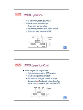
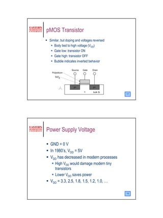
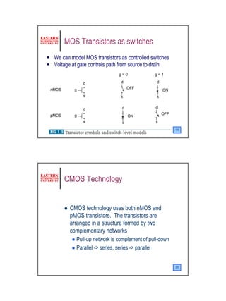
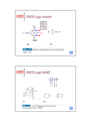
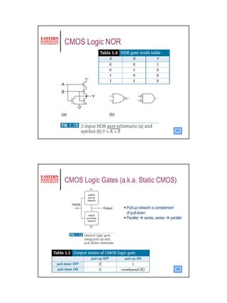
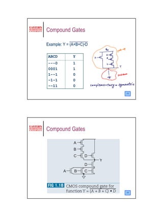
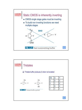
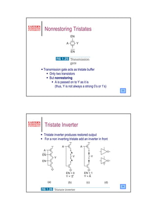
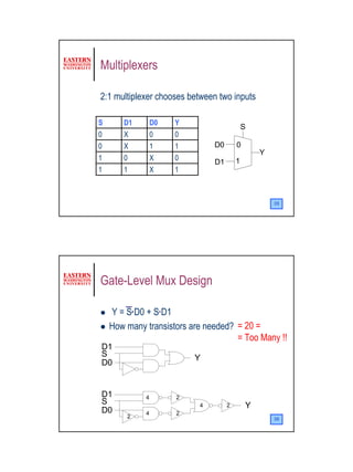
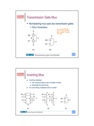
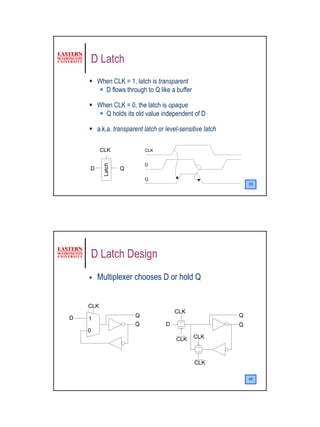
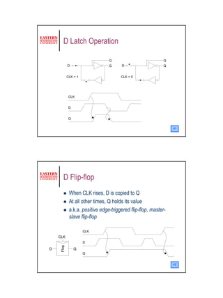
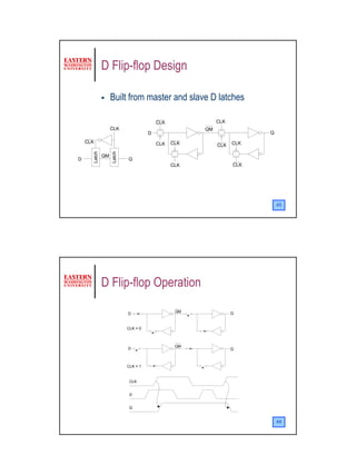
Introduction to
                     CMOS VLSI
                     Design

        Slides adapted from:

        N. Weste, D. Harris, CMOS VLSI Design,
        © Addison-Wesley, 3/e, 2004


                                                 1


     Introduction

Integrated Circuits:
many transistors on one chip
Very Large Scale Integration (VLSI):
very many transistors on one chip
Complementary Metal Oxide Semiconductor (CMOS):
fast, cheap, low power


                                                     2


                                                         1
Outline

 A Brief History
 MOS transistors
 CMOS Logic
 CMOS Fabrication and Layout
 Chip Design Challenges
      System Design
      Logic Design
      Physical Design
      Design Verification
      Fabrication, Packaging and Testing

                                                                          3


A Brief History
 T-R-A-N-S-I-S-T-O-R = TRANsfer resiSTOR

 1947: John Bardeen, Walter Brattain and William Schokley at Bell
 laboratories built the first working point contact transistor (Nobel
 Prize in Physics in 1956)
 1958: Jack Kylby built the first integrated circuit flip flop at Texas
 Instruments (Nobel Prize in Physics in 2000)
 1925: Julius Lilienfield patents the original idea of field effect
 transistors
 1935: Oskar Heil patents the first MOSFET
 1963: Frank Wanlass at Fairchild describes the first CMOS logic
 gate (nMOS and pMOS)
 1970: Processes using nMOS became dominant
 1980: Power consumption become a major issue. CMOS process
 are widely adopted.
                                                                          4


                                                                              2
A Brief History
Integrated Circuits enabled today’s way of life
1018 transistors manufactured in 2003
   100 million for every human on the planet


                                                                         5


Moore’s Law
 In 1963 Gordon Moore predicted that as a result of continuous miniaturization
 transistor count would double every 18 months
  53% compound annual growth rate over 45 years
     No other technology has grown so fast so long
 Transistors become smaller, faster, consume less power, and are
 cheaper to manufacture


                                                                         6


                                                                                 3
Clock Frequencies of Intel Processors
Transistor count is not the only factor that has grown exponentially, e.g.
clock frequencies have doubled roughly every 34 months


                                                                      7


       Chip Integration Level

          SSI = small-scale integration
          ( up to 10 gates)
          MSI = medium-scale integration
          ( up to 1000 gates)
          LSI = large-scale integration
          (up to 10000 gates)
          VLSI = very large-scale integration
          (over 10000 gates)
                                                                      8


                                                                             4
Technology Scaling

    1971: Intel 4004
    transistors with minimum dimension of 10um
    2003: Pentium 4
    transistors with minimum dimension of 130 nm

    Scaling cannot go on forever because
    transistors cannot be smaller than atoms ☺

                                                              9


 The Productivity Gap
Designers rely increasingly on design automation software tools:
• to seek productivity gains
• to cope with increased complexity


                                        Source: SEMATECH     10


                                                                   5
Silicon Lattice
 Silicon is a semiconductor
 Transistors are built on a silicon substrate
 Silicon is a Group IV material
 Forms crystal lattice with bonds to four neighbors


                                                          11


Dopants
  Pure silicon has no free carriers and conducts poorly
  Adding dopants increases the conductivity
  Group V: extra electron (n-type)
  Group III: missing electron, called hole (p-type)


        Si   Si       Si         Si   Si      Si
                  -                       +

              +                           -
        Si   As       Si         Si   B       Si

        Si   Si       Si         Si   Si      Si


                                                          12


                                                               6
Transistor Types
        Bipolar transistors
           npn or pnp silicon structure
           Small current into very thin base layer controls large
           currents between emitter and collector
           Base currents limit integration density

        Metal Oxide Semiconductor Field Effect Transistors
           nMOS and pMOS MOSFETS
           Voltage applied to insulated gate controls current
           between source and drain
           Low power allows very high integration
                                                                    13


     MOS Transistors

Four terminals: gate, source, drain, body (= bulk = substrate)


                                                                    14


                                                                         7
nMOS Operation
 Body is commonly tied to ground (0 V)
 When the gate is at a low voltage:
    P-type body is at low voltage
    Source-body and drain-body diodes are OFF
    No current flows, transistor is OFF

          Source      Gate          Drain
                                                 Polysilicon
                                                         SiO2


                                                         0
           n+                       n+
                                                 S            D
                         p          bulk Si
                                                                  15


nMOS Operation Cont.
 When the gate is at a high voltage:
   Positive charge on gate of MOS capacitor
   Negative charge attracted to body
   channel under gate gets “inverted” to n-type
   Now current can flow through n-type silicon from
   source through channel to drain, transistor is ON

                Source       Gate    Drain
                                                Polysilicon
                                                    SiO2


                                                     1
                 n+                   n+
                                                S         D
                              p       bulk Si

                                                                  16


                                                                       8
pMOS Transistor
 Similar, but doping and voltages reversed
    Body tied to high voltage (VDD)
    Gate low: transistor ON
    Gate high: transistor OFF
    Bubble indicates inverted behavior

                 Source   Gate   Drain
  Polysilicon
     SiO2


                   p+            p+

                           n     bulk Si
                                             17


Power Supply Voltage

 GND = 0 V
 In 1980’s, VDD = 5V
 VDD has decreased in modern processes
     High VDD would damage modern tiny
     transistors
     Lower VDD saves power
 VDD = 3.3, 2.5, 1.8, 1.5, 1.2, 1.0, …

                                             18


                                                  9
MOS Transistors as switches
We can model MOS transistors as controlled switches
Voltage at gate controls path from source to drain


                                                      19


    CMOS Technology


      CMOS technology uses both nMOS and
      pMOS transistors. The transistors are
      arranged in a structure formed by two
      complementary networks
         Pull-up network is complement of pull-down
         Parallel -> series, series -> parallel


                                                      20


                                                           10
CMOS Logic Inverter
                A   Y
                0   1
                1   0
         ON OFF
1= 0=       =1 =0
         OFF ON


                         21


   CMOS Logic NAND


                         22


                              11
CMOS Logic NOR


                                                23


CMOS Logic Gates (a.k.a. Static CMOS)


                    Pull-up network is complement
                    of pull-down
                    Parallel series, series parallel


                                                24


                                                       12
Compound Gates

Example: Y = (A+B+C) D

ABCD          Y
---0          1
0001          1
1--1          0
-1-1          0
--11          0
                         25


Compound Gates


                         26


                              13
How good is the output signal ?
        Signal Strength
 Strength of signal
    How close it approximates ideal voltage source
 VDD and GND rails are strongest 1 and 0 sources
 nMOS and pMOS are not ideal switches
   nMOS pass strong 0, but degraded or weak 1
   pMOS pass strong 1, but degraded or weak 0

 Thus:
    nMOS are best for pull-down network
    pMOS are best for pull-up network
                                                     27


Pass Transistors
 Transistors can be used as switches


                                                     28


                                                          14
Transmission Gates
 Pass transistors produce degraded outputs
 Transmission gates pass both 0 and 1 well


                                                   29


Static CMOS gates are fully restored

 In static CMOS, the nMOS transistors only
 need to pass 0’s and the pMOS only pass 1’s,
 so the output is always strongly driven and the
 levels are never degraded
 This is called a fully restored logic gate


                                                   30


                                                        15
Static CMOS is inherently inverting
 CMOS single stage gates must be inverting
 To build non inverting functions we need
 multiple stages


                                                       31


Tristates

 Tristate buffer produces Z when not enabled


                                     EN        A   Y
                                     0         0   Z
                                     0         1   Z
                                     1         0   0
                                     1         1   1


                                                       32


                                                            16
Nonrestoring Tristates


Transmission gate acts as tristate buffer
    Only two transistors
    But nonrestoring
        A is passed on to Y as it is
        (thus, Y is not always a strong 0’s or 1’s)
                                                        33


Tristate Inverter
Tristate inverter produces restored output
For a non inverting tristate add an inverter in front


                                                        34


                                                             17
Multiplexers

2:1 multiplexer chooses between two inputs

S      D1        D0   Y
                                            S
0      X         0    0
0      X         1    1        D0       0
                                                Y
1      0         X    0        D1       1
1      1         X    1


                                                    35


Gate-Level Mux Design

    Y = S D0 + S D1
    How many transistors are needed? = 20 =
                                     = Too Many !!
D1
S                         Y
D0


D1           4        2
S                          4        2       Y
D0           4        2
        2                                           36


                                                         18
Transmission Gate Mux
 Nonrestoring mux uses two transmission gates
     Only 4 transistors


                                                       37


Inverting Mux
 Inverting multiplexer
     Use compound gate or pair of tristate inverters
     Essentially the same thing
 For noninverting multiplexer add an inverter


                                                       38


                                                            19
D Latch
         When CLK = 1, latch is transparent
           D flows through to Q like a buffer

         When CLK = 0, the latch is opaque
           Q holds its old value independent of D

         a.k.a. transparent latch or level-sensitive latch

          CLK               CLK


                            D
           Latch


    D              Q
                            Q
                                                                 39


        D Latch Design
         Multiplexer chooses D or hold Q


    CLK
                                         CLK
D                       Q                                    Q
    1
                        Q            D                       Q
    0
                                         CLK    CLK


                                                 CLK

                                                                 40


                                                                      20
D Latch Operation

                                Q                           Q
           D                    Q     D                     Q


           CLK = 1                    CLK = 0


            CLK


            D


            Q


                                                                41


      D Flip-flop
            When CLK rises, D is copied to Q
            At all other times, Q holds its value
            a.k.a. positive edge-triggered flip-flop, master-
            slave flip-flop

                     CLK
    CLK
                     D
    Flop


D               Q
                     Q


                                                                42


                                                                     21
D Flip-flop Design

                   Built from master and slave D latches

                                         CLK              CLK
                   CLK                               QM
                                     D                                Q
    CLK                                  CLK   CLK              CLK
                                                          CLK
      Latch


                   Latch


              QM
D                          Q
                                               CLK              CLK


                                                                          43


              D Flip-flop Operation
                                                QM              Q
                           D


                           CLK = 0


                                                QM
                           D                                    Q


                           CLK = 1


                            CLK


                            D


                            Q


                                                                          44


                                                                               22
Summary

 “If the automobile had followed the same
 development cycle as the computer, a Rolls
 Royce would today cost $100, get one million
 miles per gallon, and explode once a year …”
                          Robert X. Cringely,
                          InfoWorld Magazine


                                                45


                                                     23

L1 print

  • 1.
    Introduction to CMOS VLSI Design Slides adapted from: N. Weste, D. Harris, CMOS VLSI Design, © Addison-Wesley, 3/e, 2004 1 Introduction Integrated Circuits: many transistors on one chip Very Large Scale Integration (VLSI): very many transistors on one chip Complementary Metal Oxide Semiconductor (CMOS): fast, cheap, low power 2 1
  • 2.
    Outline A BriefHistory MOS transistors CMOS Logic CMOS Fabrication and Layout Chip Design Challenges System Design Logic Design Physical Design Design Verification Fabrication, Packaging and Testing 3 A Brief History T-R-A-N-S-I-S-T-O-R = TRANsfer resiSTOR 1947: John Bardeen, Walter Brattain and William Schokley at Bell laboratories built the first working point contact transistor (Nobel Prize in Physics in 1956) 1958: Jack Kylby built the first integrated circuit flip flop at Texas Instruments (Nobel Prize in Physics in 2000) 1925: Julius Lilienfield patents the original idea of field effect transistors 1935: Oskar Heil patents the first MOSFET 1963: Frank Wanlass at Fairchild describes the first CMOS logic gate (nMOS and pMOS) 1970: Processes using nMOS became dominant 1980: Power consumption become a major issue. CMOS process are widely adopted. 4 2
  • 3.
    A Brief History IntegratedCircuits enabled today’s way of life 1018 transistors manufactured in 2003 100 million for every human on the planet 5 Moore’s Law In 1963 Gordon Moore predicted that as a result of continuous miniaturization transistor count would double every 18 months 53% compound annual growth rate over 45 years No other technology has grown so fast so long Transistors become smaller, faster, consume less power, and are cheaper to manufacture 6 3
  • 4.
    Clock Frequencies ofIntel Processors Transistor count is not the only factor that has grown exponentially, e.g. clock frequencies have doubled roughly every 34 months 7 Chip Integration Level SSI = small-scale integration ( up to 10 gates) MSI = medium-scale integration ( up to 1000 gates) LSI = large-scale integration (up to 10000 gates) VLSI = very large-scale integration (over 10000 gates) 8 4
  • 5.
    Technology Scaling 1971: Intel 4004 transistors with minimum dimension of 10um 2003: Pentium 4 transistors with minimum dimension of 130 nm Scaling cannot go on forever because transistors cannot be smaller than atoms ☺ 9 The Productivity Gap Designers rely increasingly on design automation software tools: • to seek productivity gains • to cope with increased complexity Source: SEMATECH 10 5
  • 6.
    Silicon Lattice Siliconis a semiconductor Transistors are built on a silicon substrate Silicon is a Group IV material Forms crystal lattice with bonds to four neighbors 11 Dopants Pure silicon has no free carriers and conducts poorly Adding dopants increases the conductivity Group V: extra electron (n-type) Group III: missing electron, called hole (p-type) Si Si Si Si Si Si - + + - Si As Si Si B Si Si Si Si Si Si Si 12 6
  • 7.
    Transistor Types Bipolar transistors npn or pnp silicon structure Small current into very thin base layer controls large currents between emitter and collector Base currents limit integration density Metal Oxide Semiconductor Field Effect Transistors nMOS and pMOS MOSFETS Voltage applied to insulated gate controls current between source and drain Low power allows very high integration 13 MOS Transistors Four terminals: gate, source, drain, body (= bulk = substrate) 14 7
  • 8.
    nMOS Operation Bodyis commonly tied to ground (0 V) When the gate is at a low voltage: P-type body is at low voltage Source-body and drain-body diodes are OFF No current flows, transistor is OFF Source Gate Drain Polysilicon SiO2 0 n+ n+ S D p bulk Si 15 nMOS Operation Cont. When the gate is at a high voltage: Positive charge on gate of MOS capacitor Negative charge attracted to body channel under gate gets “inverted” to n-type Now current can flow through n-type silicon from source through channel to drain, transistor is ON Source Gate Drain Polysilicon SiO2 1 n+ n+ S D p bulk Si 16 8
  • 9.
    pMOS Transistor Similar,but doping and voltages reversed Body tied to high voltage (VDD) Gate low: transistor ON Gate high: transistor OFF Bubble indicates inverted behavior Source Gate Drain Polysilicon SiO2 p+ p+ n bulk Si 17 Power Supply Voltage GND = 0 V In 1980’s, VDD = 5V VDD has decreased in modern processes High VDD would damage modern tiny transistors Lower VDD saves power VDD = 3.3, 2.5, 1.8, 1.5, 1.2, 1.0, … 18 9
  • 10.
    MOS Transistors asswitches We can model MOS transistors as controlled switches Voltage at gate controls path from source to drain 19 CMOS Technology CMOS technology uses both nMOS and pMOS transistors. The transistors are arranged in a structure formed by two complementary networks Pull-up network is complement of pull-down Parallel -> series, series -> parallel 20 10
  • 11.
    CMOS Logic Inverter A Y 0 1 1 0 ON OFF 1= 0= =1 =0 OFF ON 21 CMOS Logic NAND 22 11
  • 12.
    CMOS Logic NOR 23 CMOS Logic Gates (a.k.a. Static CMOS) Pull-up network is complement of pull-down Parallel series, series parallel 24 12
  • 13.
    Compound Gates Example: Y= (A+B+C) D ABCD Y ---0 1 0001 1 1--1 0 -1-1 0 --11 0 25 Compound Gates 26 13
  • 14.
    How good isthe output signal ? Signal Strength Strength of signal How close it approximates ideal voltage source VDD and GND rails are strongest 1 and 0 sources nMOS and pMOS are not ideal switches nMOS pass strong 0, but degraded or weak 1 pMOS pass strong 1, but degraded or weak 0 Thus: nMOS are best for pull-down network pMOS are best for pull-up network 27 Pass Transistors Transistors can be used as switches 28 14
  • 15.
    Transmission Gates Passtransistors produce degraded outputs Transmission gates pass both 0 and 1 well 29 Static CMOS gates are fully restored In static CMOS, the nMOS transistors only need to pass 0’s and the pMOS only pass 1’s, so the output is always strongly driven and the levels are never degraded This is called a fully restored logic gate 30 15
  • 16.
    Static CMOS isinherently inverting CMOS single stage gates must be inverting To build non inverting functions we need multiple stages 31 Tristates Tristate buffer produces Z when not enabled EN A Y 0 0 Z 0 1 Z 1 0 0 1 1 1 32 16
  • 17.
    Nonrestoring Tristates Transmission gateacts as tristate buffer Only two transistors But nonrestoring A is passed on to Y as it is (thus, Y is not always a strong 0’s or 1’s) 33 Tristate Inverter Tristate inverter produces restored output For a non inverting tristate add an inverter in front 34 17
  • 18.
    Multiplexers 2:1 multiplexer choosesbetween two inputs S D1 D0 Y S 0 X 0 0 0 X 1 1 D0 0 Y 1 0 X 0 D1 1 1 1 X 1 35 Gate-Level Mux Design Y = S D0 + S D1 How many transistors are needed? = 20 = = Too Many !! D1 S Y D0 D1 4 2 S 4 2 Y D0 4 2 2 36 18
  • 19.
    Transmission Gate Mux Nonrestoring mux uses two transmission gates Only 4 transistors 37 Inverting Mux Inverting multiplexer Use compound gate or pair of tristate inverters Essentially the same thing For noninverting multiplexer add an inverter 38 19
  • 20.
    D Latch When CLK = 1, latch is transparent D flows through to Q like a buffer When CLK = 0, the latch is opaque Q holds its old value independent of D a.k.a. transparent latch or level-sensitive latch CLK CLK D Latch D Q Q 39 D Latch Design Multiplexer chooses D or hold Q CLK CLK D Q Q 1 Q D Q 0 CLK CLK CLK 40 20
  • 21.
    D Latch Operation Q Q D Q D Q CLK = 1 CLK = 0 CLK D Q 41 D Flip-flop When CLK rises, D is copied to Q At all other times, Q holds its value a.k.a. positive edge-triggered flip-flop, master- slave flip-flop CLK CLK D Flop D Q Q 42 21
  • 22.
    D Flip-flop Design Built from master and slave D latches CLK CLK CLK QM D Q CLK CLK CLK CLK CLK Latch Latch QM D Q CLK CLK 43 D Flip-flop Operation QM Q D CLK = 0 QM D Q CLK = 1 CLK D Q 44 22
  • 23.
    Summary “If theautomobile had followed the same development cycle as the computer, a Rolls Royce would today cost $100, get one million miles per gallon, and explode once a year …” Robert X. Cringely, InfoWorld Magazine 45 23