Download to read offline
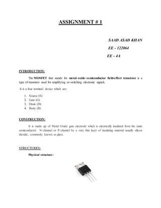
![MODES OF OPERATION:
1. Operation with zero gate voltage:
It implies that with zero voltage at both ends there is tremendous (huge) amount
of resistance (of order 1012Ω)
2. Operation with creating a channel for current flow:
It Implies that C = CoxWL
3. Operation with applying a small Vds:
It implies that rds= 1/(μnCox)(W/L)(Vgs – Vt)
4. Operation with Vds is increased:
It implies that Id = K'n(W/L)[(Vgs-V1)*Vds – ½(Vds)^2]
5. Operation with Vds > Vov:
It implies that Id = 1/2K'n(W/L)*(Vgs – V1)2
6. Operation with MOS transistor in the sub threshold region:
It implies that Vgs < Vd
CHARACTERISTICS OF MOSFETS:
1. The Id – Vds characteristic
2. The Id – Vgs characteristic
3. The finite output resistance in Saturation characteristic
4. The voltage transfer characteristic (VTC)
5. The biasing characteristic
CONFIGURATIONS OF MOSFETS:
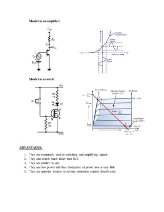
1. Mosfet as an amplifier
2. Mosfet as a switch](https://image.slidesharecdn.com/mosfetsassignment1-141023160745-conversion-gate01/85/Mosfets-5-320.jpg)


This document discusses the MOSFET (metal-oxide-semiconductor field-effect transistor). It describes the basic construction of a MOSFET including its four terminals - source, gate, drain, and body. It discusses different types of MOSFETs including depletion-mode and enhancement-mode. The working, characteristics, configurations, and advantages/disadvantages of MOSFETs are also summarized.


