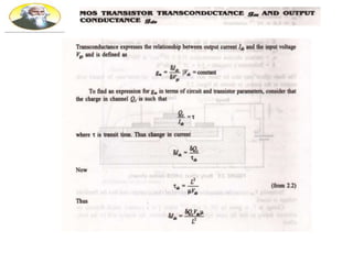
UNIT - 1
Introduction:Basic steps of IC fabrication, PMOS, NMOS, CMOS
& BiCMOS, and SOI process technologies, MOS transistors - MOS
transistor switches – Basic gate using switches, working polar
transistor Resistors and Capacitors.
Basic Electrical Properties of MOS and BiCMOS Circuits: Working
of MOS transistors – threshold voltage; MOS design equations: Ids–
Vds relationships, Threshold Voltage, Body effect, Channel length
modulation , gm, gds, figure of merit ω0; Pass transistor, NMOS
Inverter, CMOS Inverter analysis and design, Various pull ups
loads, Bi-CMOS Inverters.
VLSI DESIGN(Unit-1 )
RCEW, Pasupula (V), Nandikotkur Road, Near
Venkayapalli, KURNOOL
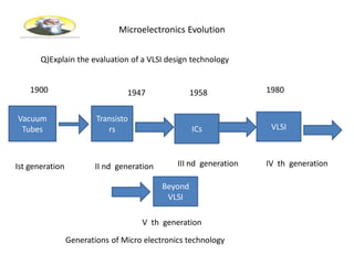
2.
Vacuum
Tubes
1900
Ist generation
Transisto
rs
II ndgeneration
1947
ICs
1958
IV th generation
VLSI
III nd generation
Beyond
VLSI
V th generation
1980
Generations of Micro electronics technology
Microelectronics Evolution
Q)Explain the evaluation of a VLSI design technology
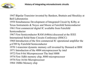
3.
History of integratingmicroelectronic circuits
1947 Bipolar Transistor invented by Bardeen, Brattain and Shockley at
Bell Laboratories
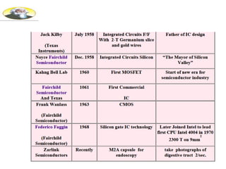
1958 Simultaneous Development of Integrated Circuit by Kilby at
Texas Instruments & Noyce and Moore at Fairchild Semiconductor
1961 First commercial digital IC available from Fairchild
Semiconductor
1967 First Semiconductor RAM (64bits) discussed at the IEEE
International Solid-State Circuits Conference (ISSCC)
1968 Introduction of the first commercial IC operational amplifier the
µA709 by Fairchild Semiconductor
1970 1-transistor dynamic memory cell invented by Dennard at IBM
1971 Introduction of the 4004 microprocessor by intel
1972 First 8-bit Microprocessor The Intel 8008
1974 First 1kBit memory chip, 8080 microprocessor
1978 First 16-bit Microprocessor
1984 1MBit Memory chip
4.
• Very-large-scale integration(VLSI): is the process of creating an integrated
circuit (IC) by combining thousands of transistors into a single chip. VLSI began in
1970s when complex semiconductor and communication technologies were being
developed. The microprocessor is a VLSI device. Before the introduction of VLSI
technology most ICs had a limited set of functions they could perform. An
electronic circuit might consist of a CPU, ROM, RAM and other glue logic. VLSI
lets IC designers add all of these into one chip.
• What are the four generations of Integration Circuits?
SSI (Small Scale Integration)
MSI (Medium Scale Integration)
LSI (Large Scale Integration)
VLSI (Very Large Scale Integration)
• What are the advantages of IC?
Size is less
High Speed
Less Power Dissipation
Q What is VLSI
5.
Level of
integration
Design
rule
No of
Transistors
YearExample
SSI 30-20 2 to 64 1960-65 Flipflops
&gates
MSI 20-10 64 to2000 1965-70 Mux,adders
LSI 10-3 1/2 2000-64000 1970-78 ROM,ROM
VLSI 3 ½ -1
1/4
64000-2
million
1978-86 16.32 bit MP
ULSI
<1 1/4 >2 million after1986 Special
purpose
processors
GSI 10 million Embedded
Systems,SOC
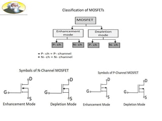
Classification of ICS
Q)Classify ICs based on Number of Transistors per chip
8.
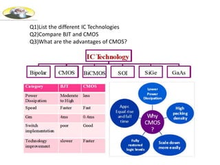
Q1)List the differentIC Technologies
Q2)Compare BJT and CMOS
Q3)What are the advantages of CMOS?
9.
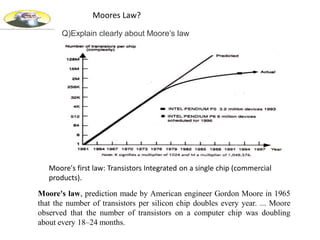
Moore's first law:Transistors Integrated on a single chip (commercial
products).
Moore's law, prediction made by American engineer Gordon Moore in 1965
that the number of transistors per silicon chip doubles every year. ... Moore
observed that the number of transistors on a computer chip was doubling
about every 18–24 months.
Moores Law?
Q)Explain clearly about Moore's law
METAL-OXIDE-SEMICONDUCTOR (MOS) ANDRELATED VLSI
TECHNOWGY
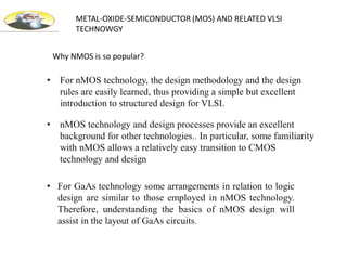
Why NMOS is so popular?
• For nMOS technology, the design methodology and the design
rules are easily learned, thus providing a simple but excellent
introduction to structured design for VLSI.
• nMOS technology and design processes provide an excellent
background for other technologies.. In particular, some familiarity
with nMOS allows a relatively easy transition to CMOS
technology and design
• For GaAs technology some arrangements in relation to logic
design are similar to those employed in nMOS technology.
Therefore, understanding the basics of nMOS design will
assist in the layout of GaAs circuits.
13.
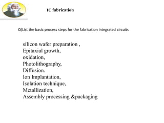
silicon wafer preparation,
Epitaxial growth,
oxidation,
Photolithography,
Diffusion.
Ion Implantation,
Isolation technique,
Metallization,
Assembly processing &packaging
IC fabrication
Q)List the basic process steps for the fabrication integrated circuits
14.
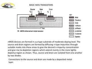
BASIC MOS TRANSISTORS
nMOSdevices are formed in a p-type substrate of moderate doping level. The
source and drain regions are formed by diffusing n-type impurities through
suitable masks into these areas to give the desired n-impurity concentration
and give rise to depletion regions which extend mainly in the more lightly
doped p-region as shown. Thus, source and drain are isolated from one another
by two diodes.
Connections to the source and drain are made by a deposited metal
layer.
15.
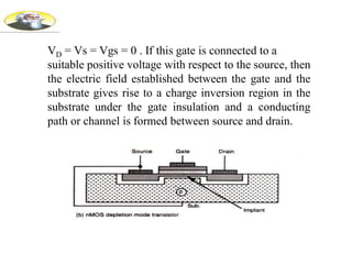
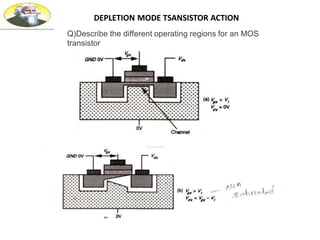
VD = Vs= Vgs = 0 . If this gate is connected to a
suitable positive voltage with respect to the source, then
the electric field established between the gate and the
substrate gives rise to a charge inversion region in the
substrate under the gate insulation and a conducting
path or channel is formed between source and drain.
16.
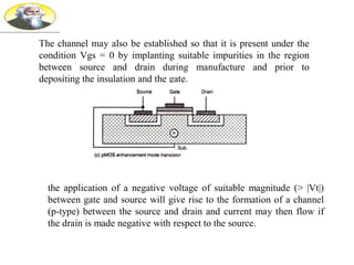
The channel mayalso be established so that it is present under the
condition Vgs = 0 by implanting suitable impurities in the region
between source and drain during manufacture and prior to
depositing the insulation and the gate.
the application of a negative voltage of suitable magnitude (> |Vt|)
between gate and source will give rise to the formation of a channel
(p-type) between the source and drain and current may then flow if
the drain is made negative with respect to the source.
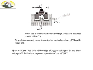
Note: Vds isthe drain-to-source voltage. Substrate assumed
connected to 0 V.
Figure:Enhancement mode transistor for particular values of Vds with
(Vgs > Vt).
Q)An n-MOSFET has threshold voltage of 1v, gate voltage of 2v and drain
voltage of 2.5v.Find the region of operation of the MOSFET.
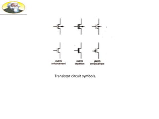
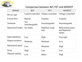
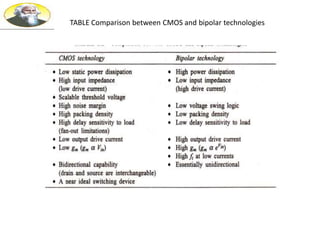
Comparison between BJT,FET and MOSFET
TERMS BJT FET MOSFET
Device type Current controlled Voltage controlled Voltage Controlled
Current flow Bipolar Unipolar Unipolar
Terminals
Not
interchangeable
Interchangeable Interchangeable
Operational modes No modes Depletion mode
only
Both Enhancement
and Depletion
modes
Input impedance Low High Very high
Output resistance Moderate Moderate Low
Operational speed Low Moderate High
Noise High Low Low
Thermal stability Low Better High
22.
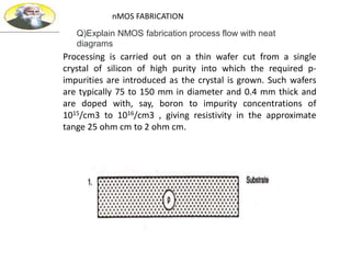
Processing is carriedout on a thin wafer cut from a single
crystal of silicon of high purity into which the required p-
impurities are introduced as the crystal is grown. Such wafers
are typically 75 to 150 mm in diameter and 0.4 mm thick and
are doped with, say, boron to impurity concentrations of
1015/cm3 to 1016/cm3 , giving resistivity in the approximate
tange 25 ohm cm to 2 ohm cm.
nMOS FABRICATION
Q)Explain NMOS fabrication process flow with neat
diagrams
23.
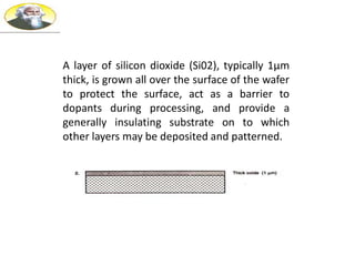
A layer ofsilicon dioxide (Si02), typically 1µm
thick, is grown all over the surface of the wafer
to protect the surface, act as a barrier to
dopants during processing, and provide a
generally insulating substrate on to which
other layers may be deposited and patterned.
24.
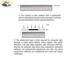
3. The surfaceis now covered with a photoresist
which is deposited onto the wafer and spun to achieve
an even distribution of the required thickness.
4. The photoresist layer is then exposed to ultraviolet light
through a mask which defines those regions into which
diffusion is to take place together with transistor channels.
Assume, for example, that those areas exposed to ultraviolet
radiation are polymerized (hardened), but that the areas
required for diffusion are shielded by the mask and remain
unaffected
25.
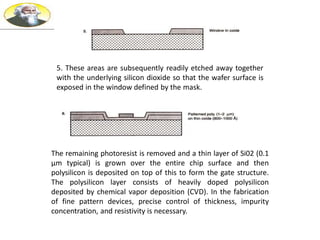
5. These areasare subsequently readily etched away together
with the underlying silicon dioxide so that the wafer surface is
exposed in the window defined by the mask.
The remaining photoresist is removed and a thin layer of Si02 (0.1
µm typical) is grown over the entire chip surface and then
polysilicon is deposited on top of this to form the gate structure.
The polysilicon layer consists of heavily doped polysilicon
deposited by chemical vapor deposition (CVD). In the fabrication
of fine pattern devices, precise control of thickness, impurity
concentration, and resistivity is necessary.
26.
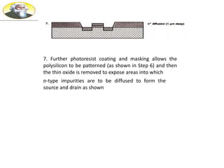
7. Further photoresistcoating and masking allows the
polysilicon to be patterned (as shown in Step 6) and then
the thin oxide is removed to expose areas into which
.
n-type impurities are to be diffused to form the
source and drain as shown
27.
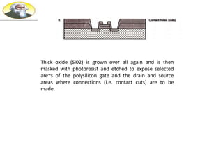
Thick oxide (Si02)is grown over all again and is then
masked with photoresist and etched to expose selected
are~s of the polysilicon gate and the drain and source
areas where connections (i.e. contact cuts) are to be
made.
28.
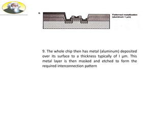
9. The wholechip then has metal (aluminum) deposited
over its surface to a thickness typically of I µm. This
metal layer is then masked and etched to form the
required interconnection pattern
29.
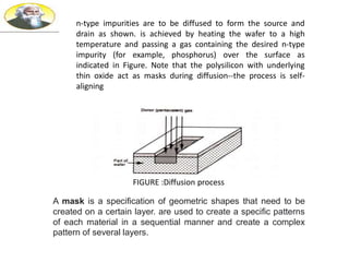
n-type impurities areto be diffused to form the source and
drain as shown. is achieved by heating the wafer to a high
temperature and passing a gas containing the desired n-type
impurity (for example, phosphorus) over the surface as
indicated in Figure. Note that the polysilicon with underlying
thin oxide act as masks during diffusion--the process is self-
aligning
FIGURE :Diffusion process
A mask is a specification of geometric shapes that need to be
created on a certain layer. are used to create a specific patterns
of each material in a sequential manner and create a complex
pattern of several layers.
30.
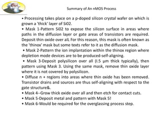
Summary of AnnMOS Process
• Processing takes place on a p-doped silicon crystal wafer on which is
grown a 'thick' layer of Si02.
• Mask 1-Pattern Si02 to expose the silicon surface in areas where
paths in the diffusion layer or gate areas of transistors are required.
Deposit thin oxide over alL For this reason, this mask is often known as
the 'thinox' mask but some texts refer to it as the diffusion mask.
• Mask 2-Pattern the ion implantation within the thinox region where
depletion mode devices are to be produced-self-aligning.
• Mask 3-Deposit polysilicon over all (I.5 µm thick typically), then
pattern using Mask 3. Using the same mask, remove thin oxide layer
where it is not covered by polysilicon.
• Diffuse n + regions into areas where thin oxide has been removed.
Transistor drains and sources are thus self-aligning with respect to the
gate structure&.
• Mask 4--Grow thick oxide over all and then etch for contact cuts.
• Mask 5-Deposit metal and pattern with Mask 5!
• Mask 6-Would be required for the overglassing process step.
31.
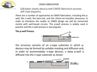
CMOS FABRICATION
There area number of approaches to CMOS fabrication, including the p-
well, the n-well, the twin-tub, and the silicon-on-insulator processes. In
order to introduce the reader to CMOS design we will be concerned
mainly with well-based circuits. The p-well process is widely used in
practice and the n-well process is also popular,
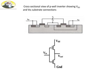
The p-well Process
the structure consists of an n-type substrate in which p-
devices may be formed by suitable masking and diffusion and,
in order to accommodate n-type devices, a deep p-well is
diffused into the n-type substrate as shown
Q)Explain clearly about p-well CMOS fabrication process
with neat diagrams.
32.
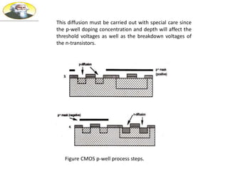
Figure CMOS p-wellprocess steps.
This diffusion must be carried out with special care since
the p-well doping concentration and depth will affect the
threshold voltages as well as the breakdown voltages of
the n-transistors.
33.
In all otherrespects-masking, patterning, and diffusion-the
process is similar to nMOS fabrication. In summary, typical
processing steps are:
Mask 1 - defines the areas in which the deep p-well diffusions are to take
place.
• Mask 2 - defines the thinox regions, namely those areas where the thick
oxide is to be stripped and thin oxide grown to accommodate p- and n-
transistors and wires.
• Mask 3 - used to pattern the polysilicon layer which is deposited after the
thin oxide.
• Mask 4 - A p-plus mask is now used (to be in effect "Anded" with Mask 2)
to define all areas where p-diffusion is to take place.
• Mask 5 - This is usually performed using the negative form of the p-plus
mask and defines those areas where n-type diffusion is to take place.
• Mask 6 - Contact cuts are now defined.
• Mask 7 - The metal layer pattern is defined by this mask.
Mask 8 - An overall passivation (overglass) layer is now applied and Mask 8
is needed to define the openings for access to bonding pads.
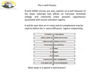
The n-well Process
N-wellCMOS circuits are also superior to p-well because of
the lower substrate bias effects on transistor threshold
voltage and inherently lower parasitic capacitances
associated with source and drain regions.
lt will be seen that an n+ mask and its complement may be
used to define the n- and p diffusions regions respectively.
Main steps in a typical n-well process~
36.
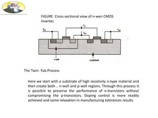
FIGURE Cross-sectional viewof n-wen CMOS
Inverter.
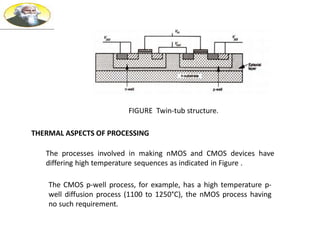
The Twin -Tub Process
Here we start with a substrate of high resistivity n-type material and
then create both .. n-well and p-well regions. Through this process it
is possib!e to preserve the performance of n-transistors without
compromising the p-transistors. Doping control is more readily
achieved and some relaxation in manufacturing tolerances results
37.
FIGURE Twin-tub structure.
THERMALASPECTS OF PROCESSING
The processes involved in making nMOS and CMOS devices have
differing high temperature sequences as indicated in Figure .
The CMOS p-well process, for example, has a high temperature p-
well diffusion process (1100 to 1250°C), the nMOS process having
no such requirement.
38.
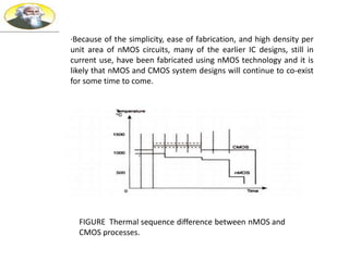
·Because of thesimplicity, ease of fabrication, and high density per
unit area of nMOS circuits, many of the earlier IC designs, still in
current use, have been fabricated using nMOS technology and it is
likely that nMOS and CMOS system designs will continue to co-exist
for some time to come.
FIGURE Thermal sequence difference between nMOS and
CMOS processes.
39.
BICMOS TECHNOWGY
A knowndeficiency of MOS technology lies in the limited load driving
capabilities of MOS transistors. This is due to the limited current sourcing and
current sinking abilities associated with both p- and n-transistors and
although it is possible, for example, to design so called super-buffers using
MOS transistors alone, such arrangements do riot always compare well with
the capabilities of bipolar transistors.
Bipolar transistors also provide higher gain and have generally better noise
and high frequency characteristics than MOS transistors and it may be seen
that BiCMOS gates could be an effective way of speeding up VLSI circuits.
However, the application of BiCMOS in sub-systems such as ALU, ROM, a
register-file, or, for that matter, a barrel shifter, is not always an effective
way of improving speed.
This is because most gates in such structures do not have to drive large
capacitive loads so that the BiCMOS arrangements give no speed
advantage.
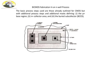
BICMOS Fabrication Inan n-well Process
The basic process steps used are those already outlined for CMOS but
with additional process steps and additional masks defining: (i) the p+
base region; (ii) n+ collector area; and (iii) the buried subcollector (BCCD).
42.
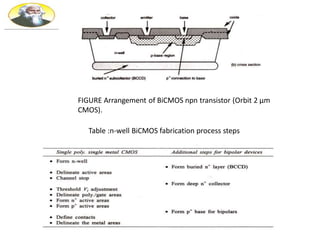
Table :n-well BiCMOSfabrication process steps
FIGURE Arrangement of BiCMOS npn transistor (Orbit 2 µm
CMOS).
43.
Basic Electrical Propertiesof MOS and BiCMOS Circuits
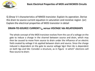
DRAIN-TO-SOURCE CURRENT Ids versus VOLTAGE Vds RELATIONSHIPS
The whole concept of the MOS transistor evolves from the use of a voltage on the
gate to induce a charge in the channel between source and drain, which may
then be caused to move from source to drain under the influence of an electric
field created by voltage V ds applied between drain and source. Since the charge
induced is dependent on the gate to source voltage Vgs• then Ids is dependent
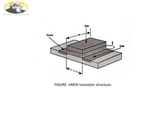
on both Vgs and Vds· Consider a structure, as in Figure in which" electrons will
flow source to drain:
Q )Draw V-I characteristics of NMOS transistor. Explain its operation. Derive
the drain to source current equation in saturation and resistive region (or)
Explain the electrical properties of MOS transistor in detail
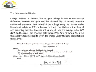
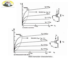
The Non-saturated Region
Chargeinduced in channel due to gate voltage is due to the voltage
difference between the gate and the channel, Vgs (assuming substrate
connected to source). Now note that the voltage along the channel varies
linearly with distance X from the source due to the IR drop in the channel
and assuming that the device is not saturated then the average value is V
ds/2. Furthermore, the effective gate voltage Vg = Vgs - Vt where Vt, is the
threshold voltage needed to invert the charge under the gate and establish
the channel
49.
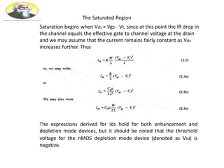
The Saturated Region
Saturationbegins when Vds = Vgs - Vt, since at this point the IR drop in
the channel equals the effective gate to channel voltage at the drain
and we may assume that the current remains fairly constant as Vds
increases further. Thus
The expressions derived for Ids hold for both enhancement and
depletion mode devices, but it should be noted that the threshold
voltage for the nMOS depletion mode device (denoted as Vtd) is
negative.
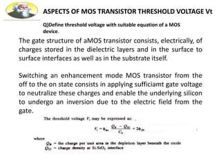
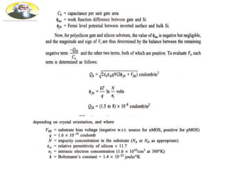
ASPECTS OF MOSTRANSISTOR THRESHOLD VOLTAGE Vt
The gate structure of aMOS transistor consists, electrically, of
charges stored in the dielectric layers and in the surface to
surface interfaces as well as in the substrate itself.
Switching an enhancement mode MOS transistor from the
off to the on state consists in applying sufficiamt gate voltage
to neutralize these charges and enable the underlying silicon
to undergo an inversion due to the electric field from the
gate.
Q)Define threshold voltage with suitable equation of a MOS
device.
53.
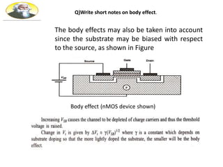
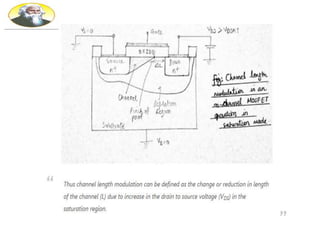
The body effectsmay also be taken into account
since the substrate may be biased with respect
to the source, as shown in Figure
Body effect (nMOS device shown)
Q)Write short notes on body effect.
56.
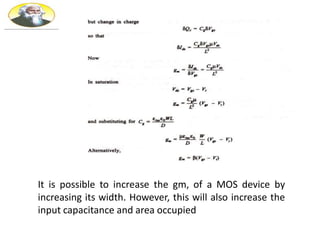
It is possibleto increase the gm, of a MOS device by
increasing its width. However, this will also increase the
input capacitance and area occupied
57.
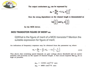
MOS TRANSISTOR FIGUREOF MERIT ω0
Q)What is the figure of merit of a MOS transistor? Mention the
suitable expression for figure of merit.
58.
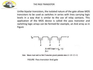
THE PASS TRANSISTOR
Unlikebipolar transistors, the isolated nature of the gate allows MOS
transistors to be used as switches in series with lines carrying logic
levels in a way that is similar to the use of relay contacts. This
application of the MOS device is called the pass transistor and
switching logic arrays can be formed-for example, an And array as in
Figure
FIGURE Pass transistor And gate
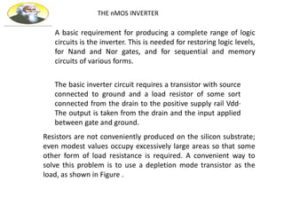
THE nMOS INVERTER
Abasic requirement for producing a complete range of logic
circuits is the inverter. This is needed for restoring logic levels,
for Nand and Nor gates, and for sequential and memory
circuits of various forms.
The basic inverter circuit requires a transistor with source
connected to ground and a load resistor of some sort
connected from the drain to the positive supply rail Vdd·
The output is taken from the drain and the input applied
between gate and ground.
Resistors are not conveniently produced on the silicon substrate;
even modest values occupy excessively large areas so that some
other form of load resistance is required. A convenient way to
solve this problem is to use a depletion mode transistor as the
load, as shown in Figure .
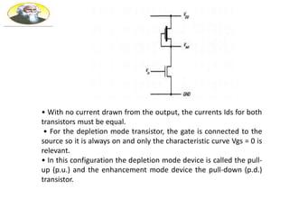
66.
• With nocurrent drawn from the output, the currents Ids for both
transistors must be equal.
• For the depletion mode transistor, the gate is connected to the
source so it is always on and only the characteristic curve Vgs = 0 is
relevant.
• In this configuration the depletion mode device is called the pull-
up (p.u.) and the enhancement mode device the pull-down (p.d.)
transistor.
67.
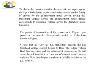
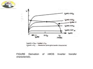
To obtain theinverter transfer characteristic we superimpose
the Vgs = 0 depletion mode characteristic curve on the family
of curves for the enhancement mode device, noting that
maximum voltage across the enhancement mode device
corresponds to minimum voltage across the depletion mode
transistor.
The points of intersection of the curves as in Figure give
points on the transfer characteristic, which is of the form
shown in Figure.
• Note that as Vin(=Vgs p.d. transistor) exceeds the p.d.
threshold voltage current begins to flow. The output voltage
Vout thus decreases and the subsequent increases in Vin will
cause the p.d. transistor to come out of saturation and become
resistive. Note that the p.u. transistor is initially resistive as the
p.d. turns on.
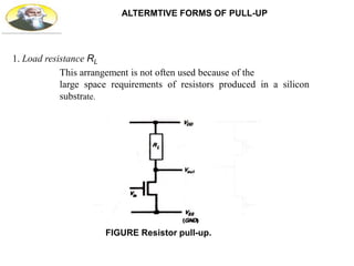
ALTERMTIVE FORMS OFPULL-UP
1. Load resistance RL
This arrangement is not often used because of the
large space requirements of resistors produced in a silicon
substrate.
FIGURE Resistor pull-up.
71.
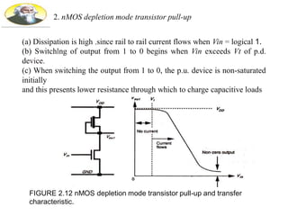
2. nMOS depletionmode transistor pull-up
(a) Dissipation is high ,since rail to rail current flows when Vin = logical 1.
(b) Switchlng of output from 1 to 0 begins when Vin exceeds Vt of p.d.
device.
(c) When switching the output from 1 to 0, the p.u. device is non-saturated
initially
and this presents lower resistance through which to charge capacitive loads
FIGURE 2.12 nMOS depletion mode transistor pull-up and transfer
characteristic.
72.
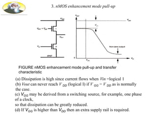
3. nMOS enhancementmode pull-up
FIGURE nMOS enhancement mode pull-up and transfer
characteristic
(a) Dissipation is high since current flows when Vin =logical 1
(b) Vout can never reach V DD (logical I) if V GG = V DD as is normally
the case.
(c) VGG may be derived from a switching source, for example, one phase
of a clock,
so that dissipation can be greatly reduced.
(d) If VGG is higher than VDD then an extra supply rail is required.
73.
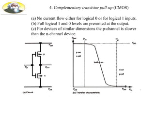
4. Complementary transistorpull-up (CMOS)
(a) No current flow either for logical 0 or for logical 1 inputs.
(b) Full logical 1 and 0 levels are presented at the output.
(c) For devices of similar dimensions the p-channel is slower
than the n-channel device.
74.
THE CMOS INVERTER
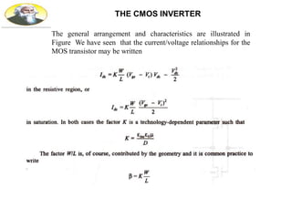
Thegeneral arrangement and characteristics are illustrated in
Figure We have seen that the current/voltage relationships for the
MOS transistor may be written
75.
where Wn andLm WP and LP are the n- and p-transistor dimensions
respectively. it may be seen that the CMOS inverter has five distinct
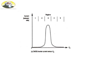
regions of operation.
77.
in region 1for which Vin . =
logic 0, we have the p-transistor fully turned on while the n-
transistor is fully turned off.
Thus no current flows through the inverter and the output is
directly connected to V DD
through the p-transistor. A good logic 1 output voltage is thus
present at the output
In region 5 Vin = logic 1, the n-transistor is fully on while the p-
transistor is fully off.
Again, no current flows and a good logic 0 appears at the output
78.
In region 2the input voltage has increased to a level which just exceeds the
threshold voltage of the n-transistor. The n-transistor conducts and has a large
voltage between source and drain; so it is in saturation. The p-transistor is also
conducting but with only a small voltage across it, it operates in the
unsaturated resistive region. A small current now flows through the inverter
from VDD to Vss. If we wish to analyze the behavior in this region, we equate
the p-device resistive region current with the n-device saturation current and
thus obtain the voltage and current relationships
Region 4 is similar to region 2 but with the roles of the p- and n-transistors
reversed. However, the current magnitudes in regions 2 and 4 are small and
most of the energy
consumed in switching from one state to the other is due to the larger current
which flows in region 3.
Region 3 is the region in which the inverter exhibits gain and in which
both transistors are in saturation.
79.
The currents ineach device must be the same: since the
transistors are in series, so we may write
from whence we can express Vin in terms of the β ~ ratio and the other
circuit voltages and currents
80.
Since both transistorsare in saturation, they act as current sources so
that the equivalent circuit in this region is two current sources in series
between VDD and Vss with the output voltage coming from their
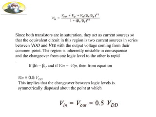
common point. The region is inherently unstable in consequence
and the changeover from one logic level to the other is rapid
.
If βn = βP and if Vtn = -Vtp, then from equation
Vin = 0.5 VDD
This implies that the changeover between logic levels is
symmetrically disposed about the point at which
82.
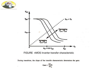
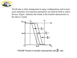
The β ratiois often unimportant in many configurations and in most
cases minimum size transistor geometries are used for both n- and p-
devices. Figure indicates the trends in the transfer characteristic as
the ratio is varied.
FIGURE Trends In transfer characteristic with β ratio
83.
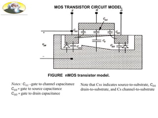
MOS TRANSISTOR CIRCUITMODEL
Notes: CGC = gate to channel capacitance
CGS = gate to source capacitance
CGD = gate to drain capacitance
Note that Css indicates source-to-substrate, CDS
drain-to-substrate, and Cs channel-to-substrate
FIGURE nMOS transistor model.
84.
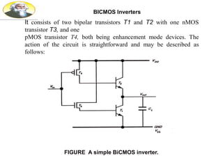
BICMOS Inverters
It consistsof two bipolar transistors T1 and T2 with one nMOS
transistor T3, and one
pMOS transistor T4, both being enhancement mode devices. The
action of the circuit is straightforward and may be described as
follows:
FIGURE A simple BiCMOS inverter.
85.
• With Vin·= 0 volts (GND) T3 is off so that T1 will be non-
conducting. But T4 is on and supplies current to the base of T2
which will conduct and act as a current source to charge the load
CL toward +5 volts(VDD). The output of the inverter will rise to
+5 volts less the · base to emitter voltage VBE of T2.
• With Vin = +5 volts(VDD) T4 is off so that T2 will be non-
conducting. But T3 will now be on and will supply current to the
base of T1 which will conduct and act as current to the load CL
discharging it toward 0 volts(GND).The output of the inverter
will follow to 0 volts plus the saturation voltage VCE Sat from the
collecter to the emitter of T1
.
86.
• The outputlogic levels will be good and will be close to the rail
voltages since V CEsat
is quite small and VBE is approximately + 0.7 volts.
• The inverter has a high input impedance.
• The inverter has a low output impedance.
• The inverter has a high current drive capability but occupies a
relatively small area.
• The inverter has high noise margins.
87.
However, owing tothe presence of a DC path from VDD to
GND through T3 and T1 this
is not a good arrangement to implement since there will be a
significant static current flow
whenever Vin = logic I.
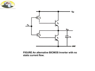
An improved version of this circuit is given in Figure , in which the
DC path through T3 and T1 is eliminated, but the output voltage
swing is now reduced, since the output cannot fall below the base
to emitter voltage VBE of T1.
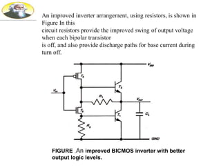
An improved inverterarrangement, using resistors, is shown in
Figure In this
circuit resistors provide the improved swing of output voltage
when each bipolar transistor
is off, and also provide discharge paths for base current during
turn off.
FIGURE ,An improved BICMOS inverter with better
output logic levels.
90.
FIGURE An ImprovedBICMOS Inverter using MOS transistors for
base current discharge
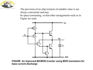
The provision of on chip resistors of suitable value is not
always convenient and may
be space-consuming, so that other arrangements-such as in
Figure are used.
91.
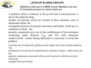
LATCH-UP IN CMOSCIRCUITS
A problem which is inherent in the p-well and n-well processes is
due to the relatively large
number of junctions which are formed in these structures and, as
mentioned earlier, the
consequent presence of parasitic transistors and diodes. Latch-up is a
condition in which . the
parasitic components give rise to the establishment of low-resistance
conducting paths between VDD and Vss with disastrous
results.Careful control during fabrication is necessary to avoid this
problem
Latch-up may be induced by glitches on the supply rails or by incident radiation.
The
mechanism involved may be understood by referring to Figure , which shows the
key
parasitic components associated with a p-well structure in which an inverter
circuit (for
example) has been formed
Q)Define Latch-up in a MOS circuit. Mention any one
of remedial process to reduce latch-up
92.
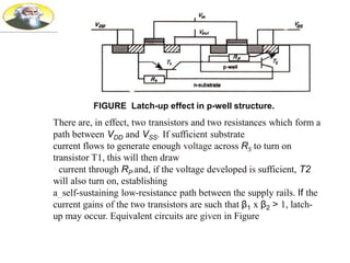
FIGURE Latch-up effectin p-well structure.
There are, in effect, two transistors and two resistances which form a
path between VDD and VSS. If sufficient substrate
current flows to generate enough voltage across RS to turn on
transistor T1, this will then draw
· current through RP and, if the voltage developed is sufficient, T2
will also turn on, establishing
a_self-sustaining low-resistance path between the supply rails. If the
current gains of the two transistors are such that β1 x β2 > 1, latch-
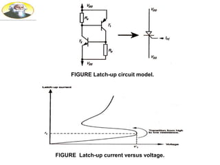
up may occur. Equivalent circuits are given in Figure
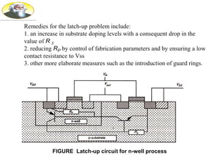
Remedies for thelatch-up problem include:
1. an increase in substrate doping levels with a consequent drop in the
value of R S
2. reducing RP by control of fabrication parameters and by ensuring a low
contact resistance to Vss
3. other more elaborate measures such as the introduction of guard rings.
FIGURE Latch-up circuit for n-well process
95.
BICMOS LATCH-UP SUSCEPTIBILITY
Onebenefit of the BiCMOS process is that it produces circuits which are
less likely to suffer from latch-up problems. This is due to several factors:
• A reduction of substrate resistance RS
• A reduction of n-well resistance Rw.
• A reduction of RS and Rw means that a larger lateral current is necessary to
invite latch-up and a higher value of holding current is also required.