SlideShare a Scribd company logo
LPC2141/42/44/46/48 Microcontrollers
Dr. P. H. Zope
Assistant Professor
SSBT’s COET Bambhori Jalgaon
North Maharashtra University Jalgaon India
phzope@gmail.com
9860631040
Study of on-chip peripherals
ADC Analog-to-Digital Converter
BOD Brown-Out Detection
CPU Central Processing Unit
DAC Digital-to-Analog Converter
DCC Debug Communications Channel
DMA Direct Memory Access
FIFO First In, First Out
GPIO General Purpose Input/Output
PLL Phase-Locked Loop
POR Power-On Reset
PWM Pulse Width Modulator
List of On-chip Devices
RAM Random Access Memory
SPI Serial Peripheral Interface
SRAM Static Random Access Memory
SSP Synchronous Serial Port
UART Universal Asynchronous Receiver/Transmitter
USB Universal Serial Bus
VPB VLSI Peripheral Bus
Key features
• 16-bit/32-bit ARM7TDMI-S microcontroller in a tiny LQFP64
package.
• 8 kB to 40 kB of on-chip static RAM and 32 kB to 512 kB of on-
chip flash memory.
• 128-bit wide interface/accelerator enables high-speed 60 MHz
operation.
• In-System Programming/In-Application Programming (ISP/IAP)
via on-chip boot loader software. Single flash sector or full chip
erase in 400 ms and programming of 256 B in 1 ms.
• Embedded ICE RT and Embedded Trace interfaces offer real-time
debugging with the on-chip Real Monitor software and high-
speed tracing of instruction execution.
• USB 2.0 Full-speed compliant device controller with 2 kB of
endpoint RAM.
• In addition, the LPC2146/48 provides 8 kB of on-chip RAM
accessible to USB by DMA.
• One or two (LPC2141/42 vs. LPC2144/46/48) 10-bit ADCs
provide a total of 6/14 analog inputs, with conversion times as
low as 2.44 ms per channel.
• Single 10-bit DAC provides variable analog output
(LPC2142/44/46/48 only).
• Two 32-bit timers/external event counters (with four capture and
four compare
channels each), PWM unit (six outputs) and watchdog.
• Low power Real-Time Clock (RTC) with independent power and
32 kHz clock input.
• Processor wake-up from Power-down mode via external interrupt.
•CPU operating voltage range of 3.0 V to 3.6 V (3.3 V ± 10 %) with 5
V tolerant I/O pads.
•Multiple serial interfaces including two UARTs (16C550), two Fast
I2C-bus (400 kbit/s), SPI and SSP with buffering and variable data
length capabilities.
• Vectored Interrupt Controller (VIC) with configurable priorities and
vector addresses.
•Up to 45 of 5 V tolerant fast general purpose I/O pins in a tiny
LQFP64 package.
•60 MHz maximum CPU clock available from programmable on-chip
PLL with settling time of 100 ms.
• On-chip integrated oscillator operates with an external crystal from
1 MHz to 25 MHz.
• Power saving modes include Idle and Power-down.
• Individual enable/disable of peripheral functions as well as
peripheral clock scaling for additional power optimization.
On-chip flash program memory
The LPC2141/42/44/46/48 incorporate a 32 kB, 64 kB, 128 kB, 256
kB and 512 kB flash memory system respectively.
On-chip static RAM
On-chip static RAM may be used for code and/or data storage.
The SRAM may be accessed as 8-bit, 16-bit, and 32-bit.
The LPC2141, LPC2142/44 and LPC2146/48 provide 8 kB, 16 kB
and 32 kB of static RAM respectively.
Memory map
10-bit ADC
LPC2144/46/48 contain two analog to digital converters.
These converters are single 10-bit successive approximation analog to digital
converters. While ADC0 has six channels, ADC1 has eight channels.
Therefore, total number of available ADC inputs for LPC2144/46/48 is 14.
Features
•10 bit successive approximation analog to digital converter.
•Measurement range of 0 V to VREF (2.0 V £ VREF £ VDDA).
•Each converter capable of performing more than 400000 10-bit samples per
second.
•Every analog input has a dedicated result register to reduce interrupt
overhead.
•Burst conversion mode for single or multiple inputs.
•Optional conversion on transition on input pin or timer match signal.
•Global Start command for both converters (LPC2142/44/46/48 only).
10-bit DAC
The DAC enables the LPC2141/42/44/46/48 to generate a variable analog output.
The maximum DAC output voltage is the VREF voltage.
Features
•10-bit DAC.
• Buffered output.
• Power-down mode available.
•Selectable speed versus power.
USB 2.0 device controller
•The USB is a 4-wire serial bus that supports communication between a host and a number
(127 max) of peripherals.
•The host controller allocates the USB bandwidth to attached devices through a token
based protocol.
•The bus supports hot plugging, unplugging, and dynamic configuration of the devices.
•All transactions are initiated by the host controller.
•The LPC2141/42/44/46/48 is equipped with a USB device controller that enables 12
Mbit/s data exchange with a USB host controller.
•It consists of a register interface, serial interface engine, endpoint buffer memory and
DMA controller.
•The serial interface engine decodes the USB data stream and writes data to the
appropriate end point buffer memory.
•The status of a completed USB transfer or error condition is indicated via status registers.
• An interrupt is also generated if enabled.
•A DMA controller (available in LPC2146/48 only) can transfer data between an endpoint
buffer and the USB RAM.
• Fully compliant with USB 2.0 Full-speed specification.
• Supports 32 physical (16 logical) endpoints.
• Supports control, bulk, interrupt and isochronous endpoints.
• Scalable realization of endpoints at run time.
• Endpoint maximum packet size selection (up to USB maximum specification) by
software at run time.
• RAM message buffer size based on endpoint realization and maximum packet size.
• Supports SoftConnect and GoodLink LED indicator. These two functions are sharing
one pin.
• Supports bus-powered capability with low suspend current.
• Supports DMA transfer on all non-control endpoints (LPC2146/48 only).
• One duplex DMA channel serves all endpoints (LPC2146/48 only).
• Allows dynamic switching between CPU controlled and DMA modes (only in
LPC2146/48).
• Double buffer implementation for bulk and isochronous endpoints.
Features
UARTs
Features
The LPC2141/42/44/46/48 each contain two UARTs. In addition to standard transmit and
receive data lines, the LPC2144/46/48 UART1 also provides a full modem control handshake
interface.
UARTs in LPC2141/42/44/46/48 introduce a fractional baud rate generator for both UARTs,
enabling these microcontrollers to achieve standard baud rates such as 115200 with any
crystal frequency above 2 MHz.
In addition, auto-CTS/RTS flow-control functions are fully implemented in hardware
• B Receive and Transmit FIFOs.
• ‘egiste lo atio s o fo to C i dust sta da d.
• ‘e ei e FIFO t igge poi ts at B, B, 8 B, a d B
• Built-in fractional baud rate generator covering wide range of baud rates without a
need for external crystals of particular values.
• T a s issio FIFO o t ol e a les i ple e tatio of soft a e XON/XOFF flo
control on both UARTs.
• LPC / / 8 UA‘T e uipped ith sta da d ode i te fa e sig als. This module
also provides full support for hardware flow control (auto-CTS/RTS).
UART0 block diagram
I2C-bus serial I/O controller
The I2C-bus is bidirectional, for inter-IC control using only two
wires: a serial clock line (SCL), and a serial data line (SDA).
Each device is recognized by a unique address and can operate as
either a receiver-only device (e.g., an LCD driver or a transmitter with
the capability to both receive and send information (such as
memory)).
Transmitters and/or receivers can operate in either master or slave
mode, depending on whether the chip has to initiate a data transfer or
is only addressed.
The I2C-bus is a multi-master bus, it can be controlled by more than
one bus master connected to it.
The I2C-bus implemented in LPC2141/42/44/46/48 supports bit rates
up to 400 kbit/s
Features
• Compliant with standard I2C-bus interface.
• Easy to configure as master, slave, or master/slave.
• Programmable clocks allow versatile rate control.
• Bidirectional data transfer between masters and slaves.
• Multi-master bus (no central master).
• Arbitration between simultaneously transmitting masters without
corruption of serial data on the bus.
• Serial clock synchronization allows devices with different bit rates to
communicate via one serial bus.
• Serial clock synchronization can be used as a handshake mechanism
to suspend and resume serial transfer.
• The I2C-bus can be used for test and diagnostic purposes.
I2C serial interface block diagram
SPI serial I/O controller
The LPC2141/42/44/46/48 each contain one SPI controller.
The SPI is a full duplex serial interface, designed to handle multiple
masters and slaves connected to a given bus.
Only a single master and a single slave can communicate on the
interface during a given data transfer.
During a data transfer the master always sends a byte of data to the
slave, and the slave always sends a byte of data to the master.
Features
• Compliant with SPI specification.
• Synchronous, Serial, Full Duplex, Communication.
• Combined SPI master and slave.
• Maximum data bit rate of one eighth of the input clock rate.
General purpose timers/external event counters
The Timer/Counter is designed to count cycles of the peripheral clock
(PCLK) or an externally supplied clock and optionally generate
interrupts or perform other actions at specified timer values, based on
four match registers.
It also includes four capture inputs to trap the timer value when an
input signal transitions, optionally generating an interrupt.
Multiple pins can be selected to perform a single capture or match
function, providing an application with ‘or’ and ‘and’, as well as
‘broadcast’ functions among them.
What is Capture ?
The Capture Control Register is used to control whether one of the
four Capture Registers is loaded with the value in the Timer Counter
when the capture event occurs, and whether an interrupt is
generated by the capture event. Setting both the rising and falling
bits at the same time is a valid configuration, resulting in a capture
event for both edges.
What is Prescaler?
The prescaler is actually a binary ripple-counter that is put before
the actual timer.
The ripple counter simply counts the clock source and provides
outputs of divide by 2, 4, 8, 16, 32 and so on.
You can select the divide ratio as the 'prescale value', and the timer
in question sees a lower frequency of the input clock.
Features
• A -bit timer/counter with a programmable 32-bit prescaler.
• E te al e e t ou te o ti e ope atio .
• Fou -bit capture channels per timer/counter that can take a
snapshot of the timer value when an input signal transitions. A capture
event may also optionally generate an interrupt.
• Fou -bit match registers that allow:
– Continuous operation with optional interrupt generation on match.
– Stop timer on match with optional interrupt generation.
– Reset timer on match with optional interrupt generation.
• Fou e te al outputs pe ti e / ou te o espo di g to at h
registers, with the following capabilities:
– Set LOW on match.
– Set HIGH on match.
– Toggle on match.
– Do nothing on match.
Watchdog timer
The purpose of the watchdog is to reset the microcontroller within a
reasonable amount of time if it enters an erroneous state. When
enabled, the watchdog will generate a system reset if the user
program fails to feed (or reload) the watchdog within a
predetermined amount of time.
Features
• Internally resets chip if not periodically reloaded.
• Debug mode.
• Enabled by software but requires a hardware reset or a watchdog
reset/interrupt to be disabled.
• Incorrect/Incomplete feed sequence causes reset/interrupt if enabled.
• Flag to indicate watchdog reset.
• Programmable 32-bit timer with internal pre-scaler.
• Selectable time period
Real-time clock
Features
The RTC is designed to provide a set of counters to measure time when normal or idle
operating mode is selected. The RTC has been designed to use little power, making it
suitable for battery powered systems where the CPU is not running continuously (Idle
mode).
• Measu es the passage of ti e to ai tai a ale da a d lo k.
• Ult a-low power design to support battery powered systems.
• P o ides Se o ds, Mi utes, Hou s, Da of Mo th, Mo th, Yea , Da of Week, and Day
of Year.
• Ca use eithe the ‘TC dedi ated kHz os illato i put o lo k de i ed f o the
external crystal/oscillator input at XTAL1. Programmable reference clock divider allows fine
adjustment of the RTC.
• Dedi ated po e suppl pi a e o e ted to a atte o the ai . V.
Pulse width modulator
The PWM is based on the standard timer block and inherits all of its features, although
only the PWM function is pinned out on the LPC2141/42/44/46/48.
The timer is designed to count cycles of the peripheral clock (PCLK) and optionally generate
interrupts or perform other actions when specified timer values occur, based on seven match
registers.
The PWM function is also based on match register events.
The ability to separately control rising and falling edge locations allows the PWM to be
used for more applications. For instance, multi-phase motor control typically requires three
non-overlapping PWM outputs with individual control of all three pulse widths and
positions.
Two match registers can be used to provide a single edge controlled PWM output.
Features
• Seven match registers allow up to six single edge controlled or three double edge controlled
PWM outputs, or a mix of both types.
• The match registers also allow:
– Continuous operation with optional interrupt generation on match.
– Stop timer on match with optional interrupt generation.
– Reset timer on match with optional interrupt generation.
• Supports single edge controlled and/or double edge controlled PWM outputs. Single edge
controlled PWM outputs all go HIGH at the beginning of each cycle unless the output is a
constant LOW. Double edge controlled PWM outputs can have either edge occur at any
position within a cycle. This allows for both positive going and negative going pulses.
• Pulse period and width can be any number of timer counts. This allows complete flexibility in
the trade-off between resolution and repetition rate. All PWM outputs will occur at the same
repetition rate.
• Double edge controlled PWM outputs can be programmed to be either positive going
or negative going pulses.
• Mat h egiste updates a e s h o ized ith pulse outputs to p e e t ge e atio of
e o eous pulses. Soft a e ust elease e at h alues efo e the a e o e
effective.
• Ma e used as a sta da d ti e if the PWM ode is ot e a led.
• A -bit Timer/Counter with a programmable 32-bit Prescaler.
PLL
The PLL accepts an input clock frequency in the range of 10 MHz to 25 MHz.
The input frequency is multiplied up into the range of 10 MHz to 60 MHz with a Current
Controlled Oscillator (CCO).
The multiplier can be an integer value from 1 to 32 (in practice, the multiplier value cannot
be higher than 6 on this family of microcontrollers due to the upper frequency limit of the
CPU).
The CCO operates in the range of 156 MHz to 320 MHz, so there is an additional divider in
the loop to keep the CCO within its frequency range while the PLL is providing the desired
output frequency.
The output divider may be set to divide by 2, 4, 8, or 16 to produce the output clock. Since
the minimum output divider value is 2, it is insured that the PLL output has a 50 % duty
cycle.
The PLL is turned off and bypassed following a chip reset and may be enabled by software.
The program must configure and activate the PLL, wait for the PLL to Lock, then connect to
the PLL as a clock source.
The PLL settling time is 100 ms.
Unit II Study of Onchip Peripherals

More Related Content

What's hot

Interfacing adc
Interfacing adcInterfacing adc
Interfacing adcPRADEEP
 
8096 microcontrollers notes
8096 microcontrollers notes8096 microcontrollers notes
8096 microcontrollers notesDr.YNM
 
Phase Shift Keying & π/4 -Quadrature Phase Shift Keying
Phase Shift Keying & π/4 -Quadrature Phase Shift KeyingPhase Shift Keying & π/4 -Quadrature Phase Shift Keying
Phase Shift Keying & π/4 -Quadrature Phase Shift Keying
Naveen Jakhar, I.T.S
 
VLSI Testing Techniques
VLSI Testing TechniquesVLSI Testing Techniques
VLSI Testing Techniques
A B Shinde
 
Memory & I/O interfacing
Memory & I/O  interfacingMemory & I/O  interfacing
Memory & I/O interfacing
deval patel
 
Task communication
Task communicationTask communication
Task communication
1jayanti
 
ARM CORTEX M3 PPT
ARM CORTEX M3 PPTARM CORTEX M3 PPT
ARM CORTEX M3 PPT
Gaurav Verma
 
Design challenges in embedded systems
Design challenges in embedded systemsDesign challenges in embedded systems
Design challenges in embedded systems
mahalakshmimalini
 
Serial Communication
Serial CommunicationSerial Communication
Serial Communication
UshaRani289
 
8051 interfacing
8051 interfacing8051 interfacing
8051 interfacing
KanchanPatil34
 
SOC System Design Approach
SOC System Design ApproachSOC System Design Approach
SOC System Design Approach
A B Shinde
 
INTRODUCTION TO MICROCONTROLLER
INTRODUCTION TO MICROCONTROLLERINTRODUCTION TO MICROCONTROLLER
INTRODUCTION TO MICROCONTROLLER
Ankita Jaiswal
 
Serial Peripheral Interface(SPI)
Serial Peripheral Interface(SPI)Serial Peripheral Interface(SPI)
Serial Peripheral Interface(SPI)
Dhaval Kaneria
 
Memory organization of 8051
Memory organization of 8051Memory organization of 8051
Memory organization of 8051Muthu Manickam
 
Hardware-Software Codesign
Hardware-Software CodesignHardware-Software Codesign
Hardware-Software Codesign
Sudhanshu Janwadkar
 
Vxworks
VxworksVxworks
8251 USART
8251 USART8251 USART
8251 USART
coolsdhanesh
 
Multiple Access
Multiple AccessMultiple Access
Multiple Access
RAVIKIRAN ANANDE
 
Introduction to Embedded Architecture
Introduction to Embedded Architecture Introduction to Embedded Architecture
Introduction to Embedded Architecture
amrutachintawar239
 
PIC 16F877A by PARTHIBAN. S.
PIC 16F877A   by PARTHIBAN. S.PIC 16F877A   by PARTHIBAN. S.
PIC 16F877A by PARTHIBAN. S.
parthi_arjun
 

What's hot (20)

Interfacing adc
Interfacing adcInterfacing adc
Interfacing adc
 
8096 microcontrollers notes
8096 microcontrollers notes8096 microcontrollers notes
8096 microcontrollers notes
 
Phase Shift Keying & π/4 -Quadrature Phase Shift Keying
Phase Shift Keying & π/4 -Quadrature Phase Shift KeyingPhase Shift Keying & π/4 -Quadrature Phase Shift Keying
Phase Shift Keying & π/4 -Quadrature Phase Shift Keying
 
VLSI Testing Techniques
VLSI Testing TechniquesVLSI Testing Techniques
VLSI Testing Techniques
 
Memory & I/O interfacing
Memory & I/O  interfacingMemory & I/O  interfacing
Memory & I/O interfacing
 
Task communication
Task communicationTask communication
Task communication
 
ARM CORTEX M3 PPT
ARM CORTEX M3 PPTARM CORTEX M3 PPT
ARM CORTEX M3 PPT
 
Design challenges in embedded systems
Design challenges in embedded systemsDesign challenges in embedded systems
Design challenges in embedded systems
 
Serial Communication
Serial CommunicationSerial Communication
Serial Communication
 
8051 interfacing
8051 interfacing8051 interfacing
8051 interfacing
 
SOC System Design Approach
SOC System Design ApproachSOC System Design Approach
SOC System Design Approach
 
INTRODUCTION TO MICROCONTROLLER
INTRODUCTION TO MICROCONTROLLERINTRODUCTION TO MICROCONTROLLER
INTRODUCTION TO MICROCONTROLLER
 
Serial Peripheral Interface(SPI)
Serial Peripheral Interface(SPI)Serial Peripheral Interface(SPI)
Serial Peripheral Interface(SPI)
 
Memory organization of 8051
Memory organization of 8051Memory organization of 8051
Memory organization of 8051
 
Hardware-Software Codesign
Hardware-Software CodesignHardware-Software Codesign
Hardware-Software Codesign
 
Vxworks
VxworksVxworks
Vxworks
 
8251 USART
8251 USART8251 USART
8251 USART
 
Multiple Access
Multiple AccessMultiple Access
Multiple Access
 
Introduction to Embedded Architecture
Introduction to Embedded Architecture Introduction to Embedded Architecture
Introduction to Embedded Architecture
 
PIC 16F877A by PARTHIBAN. S.
PIC 16F877A   by PARTHIBAN. S.PIC 16F877A   by PARTHIBAN. S.
PIC 16F877A by PARTHIBAN. S.
 

Similar to Unit II Study of Onchip Peripherals

An Overview of LPC2101/02/03
An Overview of LPC2101/02/03An Overview of LPC2101/02/03
An Overview of LPC2101/02/03
Premier Farnell
 
Overview of LPC214x MCUs
Overview of LPC214x MCUsOverview of LPC214x MCUs
Overview of LPC214x MCUs
Premier Farnell
 
Arm7 document
Arm7  documentArm7  document
Arm7 document
N Harisha
 
Overview of LPC213x MCUs
Overview of LPC213x MCUsOverview of LPC213x MCUs
Overview of LPC213x MCUs
Premier Farnell
 
Doc32059
Doc32059Doc32059
32059 sistem
32059 sistem32059 sistem
32059 sistem
Alfredo Santillan
 
Introduction of 16-Bit Automotive Microcontrollers S12XE
Introduction of 16-Bit Automotive Microcontrollers S12XEIntroduction of 16-Bit Automotive Microcontrollers S12XE
Introduction of 16-Bit Automotive Microcontrollers S12XE
Premier Farnell
 
Psoc3 text book
Psoc3 text book Psoc3 text book
Psoc3 text book
Prabhu Kiran
 
SOC Peripheral Components & SOC Tools
SOC Peripheral Components & SOC ToolsSOC Peripheral Components & SOC Tools
SOC Peripheral Components & SOC Tools
A B Shinde
 
PIC32MX5XX/6XX/7XX USB, CAN and Ethernet 32-Bit Flash Microcontrollers
PIC32MX5XX/6XX/7XX USB, CAN and Ethernet 32-Bit Flash MicrocontrollersPIC32MX5XX/6XX/7XX USB, CAN and Ethernet 32-Bit Flash Microcontrollers
PIC32MX5XX/6XX/7XX USB, CAN and Ethernet 32-Bit Flash Microcontrollers
Premier Farnell
 
Introduction to i.MX27 Multimedia Applications Processors
Introduction to i.MX27 Multimedia Applications ProcessorsIntroduction to i.MX27 Multimedia Applications Processors
Introduction to i.MX27 Multimedia Applications Processors
Premier Farnell
 
Lpc1769 68 67_66_65_64
Lpc1769 68 67_66_65_64Lpc1769 68 67_66_65_64
Lpc1769 68 67_66_65_64trowftd
 
MPC854XE: PowerQUICC III Processors
MPC854XE: PowerQUICC III ProcessorsMPC854XE: PowerQUICC III Processors
MPC854XE: PowerQUICC III Processors
Premier Farnell
 
Introduction to Stellaris Family Microcontrollers
Introduction to Stellaris Family MicrocontrollersIntroduction to Stellaris Family Microcontrollers
Introduction to Stellaris Family Microcontrollers
Premier Farnell
 
Overview Study on PIC32MX3XX / 4XX 32-Bit Controller
Overview Study on PIC32MX3XX / 4XX 32-Bit ControllerOverview Study on PIC32MX3XX / 4XX 32-Bit Controller
Overview Study on PIC32MX3XX / 4XX 32-Bit Controller
Premier Farnell
 
Introduction to intel galileo board gen2
Introduction to intel galileo board gen2Introduction to intel galileo board gen2
Introduction to intel galileo board gen2
Harshit Srivastava
 
MCF5223x: Integrated ColdFire V2 Ethernet Microcontrollers
MCF5223x: Integrated ColdFire V2 Ethernet MicrocontrollersMCF5223x: Integrated ColdFire V2 Ethernet Microcontrollers
MCF5223x: Integrated ColdFire V2 Ethernet Microcontrollers
Premier Farnell
 
Introduction to embedded systems
Introduction to embedded systemsIntroduction to embedded systems
Introduction to embedded systems
Игорь Медведев
 
dsPIC33FJ06GSXXX DSCs
dsPIC33FJ06GSXXX DSCsdsPIC33FJ06GSXXX DSCs
dsPIC33FJ06GSXXX DSCs
Premier Farnell
 
Atmega8u2 mur
Atmega8u2 murAtmega8u2 mur
Atmega8u2 mur
Nickyhoney
 

Similar to Unit II Study of Onchip Peripherals (20)

An Overview of LPC2101/02/03
An Overview of LPC2101/02/03An Overview of LPC2101/02/03
An Overview of LPC2101/02/03
 
Overview of LPC214x MCUs
Overview of LPC214x MCUsOverview of LPC214x MCUs
Overview of LPC214x MCUs
 
Arm7 document
Arm7  documentArm7  document
Arm7 document
 
Overview of LPC213x MCUs
Overview of LPC213x MCUsOverview of LPC213x MCUs
Overview of LPC213x MCUs
 
Doc32059
Doc32059Doc32059
Doc32059
 
32059 sistem
32059 sistem32059 sistem
32059 sistem
 
Introduction of 16-Bit Automotive Microcontrollers S12XE
Introduction of 16-Bit Automotive Microcontrollers S12XEIntroduction of 16-Bit Automotive Microcontrollers S12XE
Introduction of 16-Bit Automotive Microcontrollers S12XE
 
Psoc3 text book
Psoc3 text book Psoc3 text book
Psoc3 text book
 
SOC Peripheral Components & SOC Tools
SOC Peripheral Components & SOC ToolsSOC Peripheral Components & SOC Tools
SOC Peripheral Components & SOC Tools
 
PIC32MX5XX/6XX/7XX USB, CAN and Ethernet 32-Bit Flash Microcontrollers
PIC32MX5XX/6XX/7XX USB, CAN and Ethernet 32-Bit Flash MicrocontrollersPIC32MX5XX/6XX/7XX USB, CAN and Ethernet 32-Bit Flash Microcontrollers
PIC32MX5XX/6XX/7XX USB, CAN and Ethernet 32-Bit Flash Microcontrollers
 
Introduction to i.MX27 Multimedia Applications Processors
Introduction to i.MX27 Multimedia Applications ProcessorsIntroduction to i.MX27 Multimedia Applications Processors
Introduction to i.MX27 Multimedia Applications Processors
 
Lpc1769 68 67_66_65_64
Lpc1769 68 67_66_65_64Lpc1769 68 67_66_65_64
Lpc1769 68 67_66_65_64
 
MPC854XE: PowerQUICC III Processors
MPC854XE: PowerQUICC III ProcessorsMPC854XE: PowerQUICC III Processors
MPC854XE: PowerQUICC III Processors
 
Introduction to Stellaris Family Microcontrollers
Introduction to Stellaris Family MicrocontrollersIntroduction to Stellaris Family Microcontrollers
Introduction to Stellaris Family Microcontrollers
 
Overview Study on PIC32MX3XX / 4XX 32-Bit Controller
Overview Study on PIC32MX3XX / 4XX 32-Bit ControllerOverview Study on PIC32MX3XX / 4XX 32-Bit Controller
Overview Study on PIC32MX3XX / 4XX 32-Bit Controller
 
Introduction to intel galileo board gen2
Introduction to intel galileo board gen2Introduction to intel galileo board gen2
Introduction to intel galileo board gen2
 
MCF5223x: Integrated ColdFire V2 Ethernet Microcontrollers
MCF5223x: Integrated ColdFire V2 Ethernet MicrocontrollersMCF5223x: Integrated ColdFire V2 Ethernet Microcontrollers
MCF5223x: Integrated ColdFire V2 Ethernet Microcontrollers
 
Introduction to embedded systems
Introduction to embedded systemsIntroduction to embedded systems
Introduction to embedded systems
 
dsPIC33FJ06GSXXX DSCs
dsPIC33FJ06GSXXX DSCsdsPIC33FJ06GSXXX DSCs
dsPIC33FJ06GSXXX DSCs
 
Atmega8u2 mur
Atmega8u2 murAtmega8u2 mur
Atmega8u2 mur
 

More from Dr. Pankaj Zope

Unit 4 Real Time Operating System
Unit 4 Real Time Operating SystemUnit 4 Real Time Operating System
Unit 4 Real Time Operating System
Dr. Pankaj Zope
 
Unit III ARM Interface and ARM Programming
Unit III ARM Interface and ARM Programming Unit III ARM Interface and ARM Programming
Unit III ARM Interface and ARM Programming
Dr. Pankaj Zope
 
Unit ii arm7 thumb
Unit ii arm7 thumbUnit ii arm7 thumb
Unit ii arm7 thumb
Dr. Pankaj Zope
 
Unit II Arm7 Thumb Instruction
Unit II Arm7 Thumb InstructionUnit II Arm7 Thumb Instruction
Unit II Arm7 Thumb Instruction
Dr. Pankaj Zope
 
Unit II arm 7 Instruction Set
Unit II arm 7 Instruction SetUnit II arm 7 Instruction Set
Unit II arm 7 Instruction Set
Dr. Pankaj Zope
 
Unit II Arm 7 Introduction
Unit II Arm 7 IntroductionUnit II Arm 7 Introduction
Unit II Arm 7 Introduction
Dr. Pankaj Zope
 
ME Final project report setting 09-03-2015
ME Final project report setting 09-03-2015ME Final project report setting 09-03-2015
ME Final project report setting 09-03-2015
Dr. Pankaj Zope
 
BE E&TC Embedded System Manual 09 03-2015
BE E&TC Embedded System Manual 09 03-2015BE E&TC Embedded System Manual 09 03-2015
BE E&TC Embedded System Manual 09 03-2015
Dr. Pankaj Zope
 
Unit I Testing
Unit I TestingUnit I Testing
Unit I Testing
Dr. Pankaj Zope
 
Ph.d. thesis modeling and simulation of z source inverter design and its con...
Ph.d. thesis  modeling and simulation of z source inverter design and its con...Ph.d. thesis  modeling and simulation of z source inverter design and its con...
Ph.d. thesis modeling and simulation of z source inverter design and its con...
Dr. Pankaj Zope
 
Unit-I Basic Embedded System Notes
Unit-I Basic Embedded System NotesUnit-I Basic Embedded System Notes
Unit-I Basic Embedded System Notes
Dr. Pankaj Zope
 

More from Dr. Pankaj Zope (11)

Unit 4 Real Time Operating System
Unit 4 Real Time Operating SystemUnit 4 Real Time Operating System
Unit 4 Real Time Operating System
 
Unit III ARM Interface and ARM Programming
Unit III ARM Interface and ARM Programming Unit III ARM Interface and ARM Programming
Unit III ARM Interface and ARM Programming
 
Unit ii arm7 thumb
Unit ii arm7 thumbUnit ii arm7 thumb
Unit ii arm7 thumb
 
Unit II Arm7 Thumb Instruction
Unit II Arm7 Thumb InstructionUnit II Arm7 Thumb Instruction
Unit II Arm7 Thumb Instruction
 
Unit II arm 7 Instruction Set
Unit II arm 7 Instruction SetUnit II arm 7 Instruction Set
Unit II arm 7 Instruction Set
 
Unit II Arm 7 Introduction
Unit II Arm 7 IntroductionUnit II Arm 7 Introduction
Unit II Arm 7 Introduction
 
ME Final project report setting 09-03-2015
ME Final project report setting 09-03-2015ME Final project report setting 09-03-2015
ME Final project report setting 09-03-2015
 
BE E&TC Embedded System Manual 09 03-2015
BE E&TC Embedded System Manual 09 03-2015BE E&TC Embedded System Manual 09 03-2015
BE E&TC Embedded System Manual 09 03-2015
 
Unit I Testing
Unit I TestingUnit I Testing
Unit I Testing
 
Ph.d. thesis modeling and simulation of z source inverter design and its con...
Ph.d. thesis  modeling and simulation of z source inverter design and its con...Ph.d. thesis  modeling and simulation of z source inverter design and its con...
Ph.d. thesis modeling and simulation of z source inverter design and its con...
 
Unit-I Basic Embedded System Notes
Unit-I Basic Embedded System NotesUnit-I Basic Embedded System Notes
Unit-I Basic Embedded System Notes
 

Recently uploaded

一比一原版(IIT毕业证)伊利诺伊理工大学毕业证成绩单专业办理
一比一原版(IIT毕业证)伊利诺伊理工大学毕业证成绩单专业办理一比一原版(IIT毕业证)伊利诺伊理工大学毕业证成绩单专业办理
一比一原版(IIT毕业证)伊利诺伊理工大学毕业证成绩单专业办理
zwunae
 
H.Seo, ICLR 2024, MLILAB, KAIST AI.pdf
H.Seo,  ICLR 2024, MLILAB,  KAIST AI.pdfH.Seo,  ICLR 2024, MLILAB,  KAIST AI.pdf
H.Seo, ICLR 2024, MLILAB, KAIST AI.pdf
MLILAB
 
Industrial Training at Shahjalal Fertilizer Company Limited (SFCL)
Industrial Training at Shahjalal Fertilizer Company Limited (SFCL)Industrial Training at Shahjalal Fertilizer Company Limited (SFCL)
Industrial Training at Shahjalal Fertilizer Company Limited (SFCL)
MdTanvirMahtab2
 
Water Industry Process Automation and Control Monthly - May 2024.pdf
Water Industry Process Automation and Control Monthly - May 2024.pdfWater Industry Process Automation and Control Monthly - May 2024.pdf
Water Industry Process Automation and Control Monthly - May 2024.pdf
Water Industry Process Automation & Control
 
WATER CRISIS and its solutions-pptx 1234
WATER CRISIS and its solutions-pptx 1234WATER CRISIS and its solutions-pptx 1234
WATER CRISIS and its solutions-pptx 1234
AafreenAbuthahir2
 
space technology lecture notes on satellite
space technology lecture notes on satellitespace technology lecture notes on satellite
space technology lecture notes on satellite
ongomchris
 
block diagram and signal flow graph representation
block diagram and signal flow graph representationblock diagram and signal flow graph representation
block diagram and signal flow graph representation
Divya Somashekar
 
MCQ Soil mechanics questions (Soil shear strength).pdf
MCQ Soil mechanics questions (Soil shear strength).pdfMCQ Soil mechanics questions (Soil shear strength).pdf
MCQ Soil mechanics questions (Soil shear strength).pdf
Osamah Alsalih
 
Runway Orientation Based on the Wind Rose Diagram.pptx
Runway Orientation Based on the Wind Rose Diagram.pptxRunway Orientation Based on the Wind Rose Diagram.pptx
Runway Orientation Based on the Wind Rose Diagram.pptx
SupreethSP4
 
Cosmetic shop management system project report.pdf
Cosmetic shop management system project report.pdfCosmetic shop management system project report.pdf
Cosmetic shop management system project report.pdf
Kamal Acharya
 
Railway Signalling Principles Edition 3.pdf
Railway Signalling Principles Edition 3.pdfRailway Signalling Principles Edition 3.pdf
Railway Signalling Principles Edition 3.pdf
TeeVichai
 
The Benefits and Techniques of Trenchless Pipe Repair.pdf
The Benefits and Techniques of Trenchless Pipe Repair.pdfThe Benefits and Techniques of Trenchless Pipe Repair.pdf
The Benefits and Techniques of Trenchless Pipe Repair.pdf
Pipe Restoration Solutions
 
power quality voltage fluctuation UNIT - I.pptx
power quality voltage fluctuation UNIT - I.pptxpower quality voltage fluctuation UNIT - I.pptx
power quality voltage fluctuation UNIT - I.pptx
ViniHema
 
Sachpazis:Terzaghi Bearing Capacity Estimation in simple terms with Calculati...
Sachpazis:Terzaghi Bearing Capacity Estimation in simple terms with Calculati...Sachpazis:Terzaghi Bearing Capacity Estimation in simple terms with Calculati...
Sachpazis:Terzaghi Bearing Capacity Estimation in simple terms with Calculati...
Dr.Costas Sachpazis
 
在线办理(ANU毕业证书)澳洲国立大学毕业证录取通知书一模一样
在线办理(ANU毕业证书)澳洲国立大学毕业证录取通知书一模一样在线办理(ANU毕业证书)澳洲国立大学毕业证录取通知书一模一样
在线办理(ANU毕业证书)澳洲国立大学毕业证录取通知书一模一样
obonagu
 
DESIGN A COTTON SEED SEPARATION MACHINE.docx
DESIGN A COTTON SEED SEPARATION MACHINE.docxDESIGN A COTTON SEED SEPARATION MACHINE.docx
DESIGN A COTTON SEED SEPARATION MACHINE.docx
FluxPrime1
 
Standard Reomte Control Interface - Neometrix
Standard Reomte Control Interface - NeometrixStandard Reomte Control Interface - Neometrix
Standard Reomte Control Interface - Neometrix
Neometrix_Engineering_Pvt_Ltd
 
ML for identifying fraud using open blockchain data.pptx
ML for identifying fraud using open blockchain data.pptxML for identifying fraud using open blockchain data.pptx
ML for identifying fraud using open blockchain data.pptx
Vijay Dialani, PhD
 
ASME IX(9) 2007 Full Version .pdf
ASME IX(9)  2007 Full Version       .pdfASME IX(9)  2007 Full Version       .pdf
ASME IX(9) 2007 Full Version .pdf
AhmedHussein950959
 
Design and Analysis of Algorithms-DP,Backtracking,Graphs,B&B
Design and Analysis of Algorithms-DP,Backtracking,Graphs,B&BDesign and Analysis of Algorithms-DP,Backtracking,Graphs,B&B
Design and Analysis of Algorithms-DP,Backtracking,Graphs,B&B
Sreedhar Chowdam
 

Recently uploaded (20)

一比一原版(IIT毕业证)伊利诺伊理工大学毕业证成绩单专业办理
一比一原版(IIT毕业证)伊利诺伊理工大学毕业证成绩单专业办理一比一原版(IIT毕业证)伊利诺伊理工大学毕业证成绩单专业办理
一比一原版(IIT毕业证)伊利诺伊理工大学毕业证成绩单专业办理
 
H.Seo, ICLR 2024, MLILAB, KAIST AI.pdf
H.Seo,  ICLR 2024, MLILAB,  KAIST AI.pdfH.Seo,  ICLR 2024, MLILAB,  KAIST AI.pdf
H.Seo, ICLR 2024, MLILAB, KAIST AI.pdf
 
Industrial Training at Shahjalal Fertilizer Company Limited (SFCL)
Industrial Training at Shahjalal Fertilizer Company Limited (SFCL)Industrial Training at Shahjalal Fertilizer Company Limited (SFCL)
Industrial Training at Shahjalal Fertilizer Company Limited (SFCL)
 
Water Industry Process Automation and Control Monthly - May 2024.pdf
Water Industry Process Automation and Control Monthly - May 2024.pdfWater Industry Process Automation and Control Monthly - May 2024.pdf
Water Industry Process Automation and Control Monthly - May 2024.pdf
 
WATER CRISIS and its solutions-pptx 1234
WATER CRISIS and its solutions-pptx 1234WATER CRISIS and its solutions-pptx 1234
WATER CRISIS and its solutions-pptx 1234
 
space technology lecture notes on satellite
space technology lecture notes on satellitespace technology lecture notes on satellite
space technology lecture notes on satellite
 
block diagram and signal flow graph representation
block diagram and signal flow graph representationblock diagram and signal flow graph representation
block diagram and signal flow graph representation
 
MCQ Soil mechanics questions (Soil shear strength).pdf
MCQ Soil mechanics questions (Soil shear strength).pdfMCQ Soil mechanics questions (Soil shear strength).pdf
MCQ Soil mechanics questions (Soil shear strength).pdf
 
Runway Orientation Based on the Wind Rose Diagram.pptx
Runway Orientation Based on the Wind Rose Diagram.pptxRunway Orientation Based on the Wind Rose Diagram.pptx
Runway Orientation Based on the Wind Rose Diagram.pptx
 
Cosmetic shop management system project report.pdf
Cosmetic shop management system project report.pdfCosmetic shop management system project report.pdf
Cosmetic shop management system project report.pdf
 
Railway Signalling Principles Edition 3.pdf
Railway Signalling Principles Edition 3.pdfRailway Signalling Principles Edition 3.pdf
Railway Signalling Principles Edition 3.pdf
 
The Benefits and Techniques of Trenchless Pipe Repair.pdf
The Benefits and Techniques of Trenchless Pipe Repair.pdfThe Benefits and Techniques of Trenchless Pipe Repair.pdf
The Benefits and Techniques of Trenchless Pipe Repair.pdf
 
power quality voltage fluctuation UNIT - I.pptx
power quality voltage fluctuation UNIT - I.pptxpower quality voltage fluctuation UNIT - I.pptx
power quality voltage fluctuation UNIT - I.pptx
 
Sachpazis:Terzaghi Bearing Capacity Estimation in simple terms with Calculati...
Sachpazis:Terzaghi Bearing Capacity Estimation in simple terms with Calculati...Sachpazis:Terzaghi Bearing Capacity Estimation in simple terms with Calculati...
Sachpazis:Terzaghi Bearing Capacity Estimation in simple terms with Calculati...
 
在线办理(ANU毕业证书)澳洲国立大学毕业证录取通知书一模一样
在线办理(ANU毕业证书)澳洲国立大学毕业证录取通知书一模一样在线办理(ANU毕业证书)澳洲国立大学毕业证录取通知书一模一样
在线办理(ANU毕业证书)澳洲国立大学毕业证录取通知书一模一样
 
DESIGN A COTTON SEED SEPARATION MACHINE.docx
DESIGN A COTTON SEED SEPARATION MACHINE.docxDESIGN A COTTON SEED SEPARATION MACHINE.docx
DESIGN A COTTON SEED SEPARATION MACHINE.docx
 
Standard Reomte Control Interface - Neometrix
Standard Reomte Control Interface - NeometrixStandard Reomte Control Interface - Neometrix
Standard Reomte Control Interface - Neometrix
 
ML for identifying fraud using open blockchain data.pptx
ML for identifying fraud using open blockchain data.pptxML for identifying fraud using open blockchain data.pptx
ML for identifying fraud using open blockchain data.pptx
 
ASME IX(9) 2007 Full Version .pdf
ASME IX(9)  2007 Full Version       .pdfASME IX(9)  2007 Full Version       .pdf
ASME IX(9) 2007 Full Version .pdf
 
Design and Analysis of Algorithms-DP,Backtracking,Graphs,B&B
Design and Analysis of Algorithms-DP,Backtracking,Graphs,B&BDesign and Analysis of Algorithms-DP,Backtracking,Graphs,B&B
Design and Analysis of Algorithms-DP,Backtracking,Graphs,B&B
 

Unit II Study of Onchip Peripherals

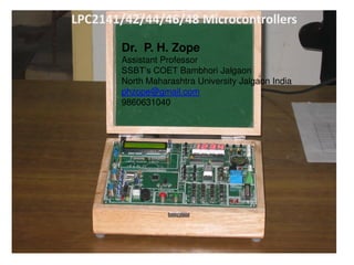
  • 1. LPC2141/42/44/46/48 Microcontrollers Dr. P. H. Zope Assistant Professor SSBT’s COET Bambhori Jalgaon North Maharashtra University Jalgaon India phzope@gmail.com 9860631040
  • 2.
  • 3. Study of on-chip peripherals
  • 4. ADC Analog-to-Digital Converter BOD Brown-Out Detection CPU Central Processing Unit DAC Digital-to-Analog Converter DCC Debug Communications Channel DMA Direct Memory Access FIFO First In, First Out GPIO General Purpose Input/Output PLL Phase-Locked Loop POR Power-On Reset PWM Pulse Width Modulator List of On-chip Devices
  • 5. RAM Random Access Memory SPI Serial Peripheral Interface SRAM Static Random Access Memory SSP Synchronous Serial Port UART Universal Asynchronous Receiver/Transmitter USB Universal Serial Bus VPB VLSI Peripheral Bus
  • 6. Key features • 16-bit/32-bit ARM7TDMI-S microcontroller in a tiny LQFP64 package. • 8 kB to 40 kB of on-chip static RAM and 32 kB to 512 kB of on- chip flash memory. • 128-bit wide interface/accelerator enables high-speed 60 MHz operation. • In-System Programming/In-Application Programming (ISP/IAP) via on-chip boot loader software. Single flash sector or full chip erase in 400 ms and programming of 256 B in 1 ms. • Embedded ICE RT and Embedded Trace interfaces offer real-time debugging with the on-chip Real Monitor software and high- speed tracing of instruction execution. • USB 2.0 Full-speed compliant device controller with 2 kB of endpoint RAM.
  • 7. • In addition, the LPC2146/48 provides 8 kB of on-chip RAM accessible to USB by DMA. • One or two (LPC2141/42 vs. LPC2144/46/48) 10-bit ADCs provide a total of 6/14 analog inputs, with conversion times as low as 2.44 ms per channel. • Single 10-bit DAC provides variable analog output (LPC2142/44/46/48 only). • Two 32-bit timers/external event counters (with four capture and four compare channels each), PWM unit (six outputs) and watchdog. • Low power Real-Time Clock (RTC) with independent power and 32 kHz clock input. • Processor wake-up from Power-down mode via external interrupt. •CPU operating voltage range of 3.0 V to 3.6 V (3.3 V ± 10 %) with 5 V tolerant I/O pads.
  • 8. •Multiple serial interfaces including two UARTs (16C550), two Fast I2C-bus (400 kbit/s), SPI and SSP with buffering and variable data length capabilities. • Vectored Interrupt Controller (VIC) with configurable priorities and vector addresses. •Up to 45 of 5 V tolerant fast general purpose I/O pins in a tiny LQFP64 package. •60 MHz maximum CPU clock available from programmable on-chip PLL with settling time of 100 ms. • On-chip integrated oscillator operates with an external crystal from 1 MHz to 25 MHz. • Power saving modes include Idle and Power-down. • Individual enable/disable of peripheral functions as well as peripheral clock scaling for additional power optimization.
  • 9.
  • 10.
  • 11. On-chip flash program memory The LPC2141/42/44/46/48 incorporate a 32 kB, 64 kB, 128 kB, 256 kB and 512 kB flash memory system respectively. On-chip static RAM On-chip static RAM may be used for code and/or data storage. The SRAM may be accessed as 8-bit, 16-bit, and 32-bit. The LPC2141, LPC2142/44 and LPC2146/48 provide 8 kB, 16 kB and 32 kB of static RAM respectively.
  • 13. 10-bit ADC LPC2144/46/48 contain two analog to digital converters. These converters are single 10-bit successive approximation analog to digital converters. While ADC0 has six channels, ADC1 has eight channels. Therefore, total number of available ADC inputs for LPC2144/46/48 is 14. Features •10 bit successive approximation analog to digital converter. •Measurement range of 0 V to VREF (2.0 V £ VREF £ VDDA). •Each converter capable of performing more than 400000 10-bit samples per second. •Every analog input has a dedicated result register to reduce interrupt overhead. •Burst conversion mode for single or multiple inputs. •Optional conversion on transition on input pin or timer match signal. •Global Start command for both converters (LPC2142/44/46/48 only).
  • 14.
  • 15. 10-bit DAC The DAC enables the LPC2141/42/44/46/48 to generate a variable analog output. The maximum DAC output voltage is the VREF voltage. Features •10-bit DAC. • Buffered output. • Power-down mode available. •Selectable speed versus power.
  • 16. USB 2.0 device controller •The USB is a 4-wire serial bus that supports communication between a host and a number (127 max) of peripherals. •The host controller allocates the USB bandwidth to attached devices through a token based protocol. •The bus supports hot plugging, unplugging, and dynamic configuration of the devices. •All transactions are initiated by the host controller.
  • 17. •The LPC2141/42/44/46/48 is equipped with a USB device controller that enables 12 Mbit/s data exchange with a USB host controller. •It consists of a register interface, serial interface engine, endpoint buffer memory and DMA controller. •The serial interface engine decodes the USB data stream and writes data to the appropriate end point buffer memory. •The status of a completed USB transfer or error condition is indicated via status registers. • An interrupt is also generated if enabled. •A DMA controller (available in LPC2146/48 only) can transfer data between an endpoint buffer and the USB RAM.
  • 18. • Fully compliant with USB 2.0 Full-speed specification. • Supports 32 physical (16 logical) endpoints. • Supports control, bulk, interrupt and isochronous endpoints. • Scalable realization of endpoints at run time. • Endpoint maximum packet size selection (up to USB maximum specification) by software at run time. • RAM message buffer size based on endpoint realization and maximum packet size. • Supports SoftConnect and GoodLink LED indicator. These two functions are sharing one pin. • Supports bus-powered capability with low suspend current. • Supports DMA transfer on all non-control endpoints (LPC2146/48 only). • One duplex DMA channel serves all endpoints (LPC2146/48 only). • Allows dynamic switching between CPU controlled and DMA modes (only in LPC2146/48). • Double buffer implementation for bulk and isochronous endpoints. Features
  • 19. UARTs Features The LPC2141/42/44/46/48 each contain two UARTs. In addition to standard transmit and receive data lines, the LPC2144/46/48 UART1 also provides a full modem control handshake interface. UARTs in LPC2141/42/44/46/48 introduce a fractional baud rate generator for both UARTs, enabling these microcontrollers to achieve standard baud rates such as 115200 with any crystal frequency above 2 MHz. In addition, auto-CTS/RTS flow-control functions are fully implemented in hardware • B Receive and Transmit FIFOs. • ‘egiste lo atio s o fo to C i dust sta da d. • ‘e ei e FIFO t igge poi ts at B, B, 8 B, a d B • Built-in fractional baud rate generator covering wide range of baud rates without a need for external crystals of particular values. • T a s issio FIFO o t ol e a les i ple e tatio of soft a e XON/XOFF flo control on both UARTs. • LPC / / 8 UA‘T e uipped ith sta da d ode i te fa e sig als. This module also provides full support for hardware flow control (auto-CTS/RTS).
  • 21. I2C-bus serial I/O controller The I2C-bus is bidirectional, for inter-IC control using only two wires: a serial clock line (SCL), and a serial data line (SDA). Each device is recognized by a unique address and can operate as either a receiver-only device (e.g., an LCD driver or a transmitter with the capability to both receive and send information (such as memory)). Transmitters and/or receivers can operate in either master or slave mode, depending on whether the chip has to initiate a data transfer or is only addressed. The I2C-bus is a multi-master bus, it can be controlled by more than one bus master connected to it. The I2C-bus implemented in LPC2141/42/44/46/48 supports bit rates up to 400 kbit/s
  • 22. Features • Compliant with standard I2C-bus interface. • Easy to configure as master, slave, or master/slave. • Programmable clocks allow versatile rate control. • Bidirectional data transfer between masters and slaves. • Multi-master bus (no central master). • Arbitration between simultaneously transmitting masters without corruption of serial data on the bus. • Serial clock synchronization allows devices with different bit rates to communicate via one serial bus. • Serial clock synchronization can be used as a handshake mechanism to suspend and resume serial transfer. • The I2C-bus can be used for test and diagnostic purposes.
  • 23.
  • 24. I2C serial interface block diagram
  • 25. SPI serial I/O controller The LPC2141/42/44/46/48 each contain one SPI controller. The SPI is a full duplex serial interface, designed to handle multiple masters and slaves connected to a given bus. Only a single master and a single slave can communicate on the interface during a given data transfer. During a data transfer the master always sends a byte of data to the slave, and the slave always sends a byte of data to the master.
  • 26. Features • Compliant with SPI specification. • Synchronous, Serial, Full Duplex, Communication. • Combined SPI master and slave. • Maximum data bit rate of one eighth of the input clock rate.
  • 27.
  • 28. General purpose timers/external event counters The Timer/Counter is designed to count cycles of the peripheral clock (PCLK) or an externally supplied clock and optionally generate interrupts or perform other actions at specified timer values, based on four match registers. It also includes four capture inputs to trap the timer value when an input signal transitions, optionally generating an interrupt. Multiple pins can be selected to perform a single capture or match function, providing an application with ‘or’ and ‘and’, as well as ‘broadcast’ functions among them.
  • 29. What is Capture ? The Capture Control Register is used to control whether one of the four Capture Registers is loaded with the value in the Timer Counter when the capture event occurs, and whether an interrupt is generated by the capture event. Setting both the rising and falling bits at the same time is a valid configuration, resulting in a capture event for both edges. What is Prescaler? The prescaler is actually a binary ripple-counter that is put before the actual timer. The ripple counter simply counts the clock source and provides outputs of divide by 2, 4, 8, 16, 32 and so on. You can select the divide ratio as the 'prescale value', and the timer in question sees a lower frequency of the input clock.
  • 30. Features • A -bit timer/counter with a programmable 32-bit prescaler. • E te al e e t ou te o ti e ope atio . • Fou -bit capture channels per timer/counter that can take a snapshot of the timer value when an input signal transitions. A capture event may also optionally generate an interrupt. • Fou -bit match registers that allow: – Continuous operation with optional interrupt generation on match. – Stop timer on match with optional interrupt generation. – Reset timer on match with optional interrupt generation. • Fou e te al outputs pe ti e / ou te o espo di g to at h registers, with the following capabilities: – Set LOW on match. – Set HIGH on match. – Toggle on match. – Do nothing on match.
  • 31.
  • 32. Watchdog timer The purpose of the watchdog is to reset the microcontroller within a reasonable amount of time if it enters an erroneous state. When enabled, the watchdog will generate a system reset if the user program fails to feed (or reload) the watchdog within a predetermined amount of time.
  • 33. Features • Internally resets chip if not periodically reloaded. • Debug mode. • Enabled by software but requires a hardware reset or a watchdog reset/interrupt to be disabled. • Incorrect/Incomplete feed sequence causes reset/interrupt if enabled. • Flag to indicate watchdog reset. • Programmable 32-bit timer with internal pre-scaler. • Selectable time period
  • 34.
  • 35. Real-time clock Features The RTC is designed to provide a set of counters to measure time when normal or idle operating mode is selected. The RTC has been designed to use little power, making it suitable for battery powered systems where the CPU is not running continuously (Idle mode). • Measu es the passage of ti e to ai tai a ale da a d lo k. • Ult a-low power design to support battery powered systems. • P o ides Se o ds, Mi utes, Hou s, Da of Mo th, Mo th, Yea , Da of Week, and Day of Year. • Ca use eithe the ‘TC dedi ated kHz os illato i put o lo k de i ed f o the external crystal/oscillator input at XTAL1. Programmable reference clock divider allows fine adjustment of the RTC. • Dedi ated po e suppl pi a e o e ted to a atte o the ai . V.
  • 36.
  • 37. Pulse width modulator The PWM is based on the standard timer block and inherits all of its features, although only the PWM function is pinned out on the LPC2141/42/44/46/48. The timer is designed to count cycles of the peripheral clock (PCLK) and optionally generate interrupts or perform other actions when specified timer values occur, based on seven match registers. The PWM function is also based on match register events. The ability to separately control rising and falling edge locations allows the PWM to be used for more applications. For instance, multi-phase motor control typically requires three non-overlapping PWM outputs with individual control of all three pulse widths and positions. Two match registers can be used to provide a single edge controlled PWM output.
  • 38. Features • Seven match registers allow up to six single edge controlled or three double edge controlled PWM outputs, or a mix of both types. • The match registers also allow: – Continuous operation with optional interrupt generation on match. – Stop timer on match with optional interrupt generation. – Reset timer on match with optional interrupt generation. • Supports single edge controlled and/or double edge controlled PWM outputs. Single edge controlled PWM outputs all go HIGH at the beginning of each cycle unless the output is a constant LOW. Double edge controlled PWM outputs can have either edge occur at any position within a cycle. This allows for both positive going and negative going pulses. • Pulse period and width can be any number of timer counts. This allows complete flexibility in the trade-off between resolution and repetition rate. All PWM outputs will occur at the same repetition rate. • Double edge controlled PWM outputs can be programmed to be either positive going or negative going pulses. • Mat h egiste updates a e s h o ized ith pulse outputs to p e e t ge e atio of e o eous pulses. Soft a e ust elease e at h alues efo e the a e o e effective. • Ma e used as a sta da d ti e if the PWM ode is ot e a led. • A -bit Timer/Counter with a programmable 32-bit Prescaler.
  • 39.
  • 40. PLL The PLL accepts an input clock frequency in the range of 10 MHz to 25 MHz. The input frequency is multiplied up into the range of 10 MHz to 60 MHz with a Current Controlled Oscillator (CCO). The multiplier can be an integer value from 1 to 32 (in practice, the multiplier value cannot be higher than 6 on this family of microcontrollers due to the upper frequency limit of the CPU). The CCO operates in the range of 156 MHz to 320 MHz, so there is an additional divider in the loop to keep the CCO within its frequency range while the PLL is providing the desired output frequency. The output divider may be set to divide by 2, 4, 8, or 16 to produce the output clock. Since the minimum output divider value is 2, it is insured that the PLL output has a 50 % duty cycle. The PLL is turned off and bypassed following a chip reset and may be enabled by software. The program must configure and activate the PLL, wait for the PLL to Lock, then connect to the PLL as a clock source. The PLL settling time is 100 ms.