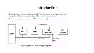
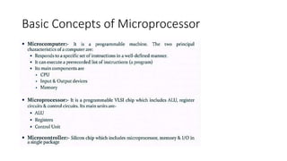
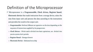
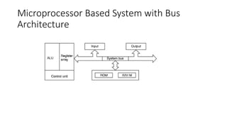
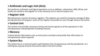
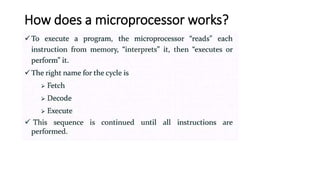
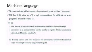
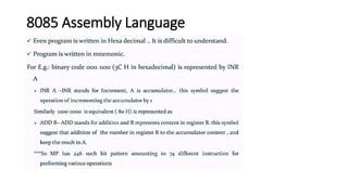
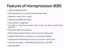
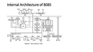
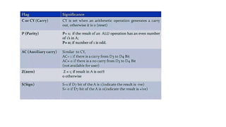
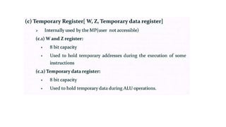
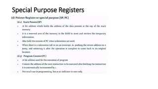
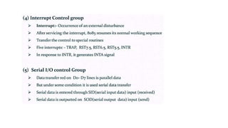
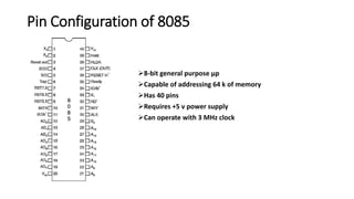
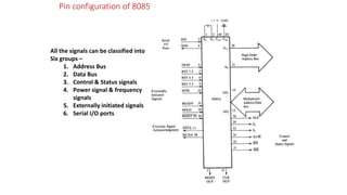
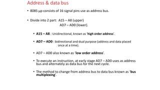
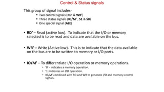
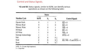
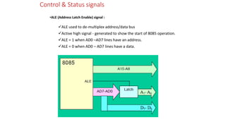
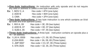
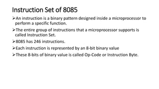
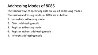
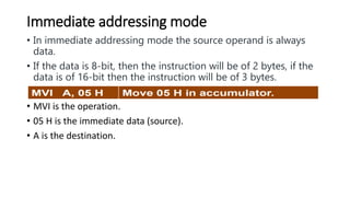
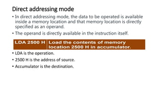
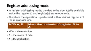
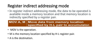
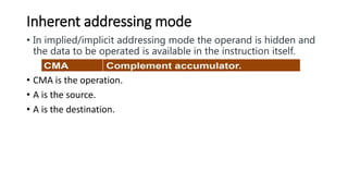
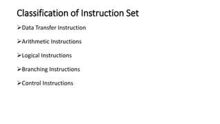
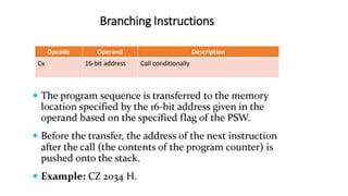
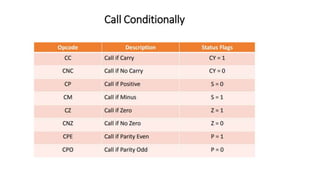
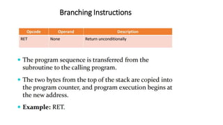
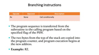
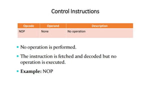
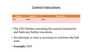
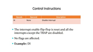
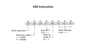
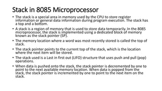
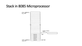
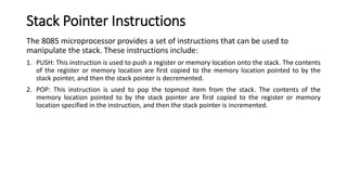
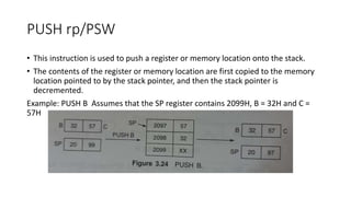
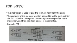
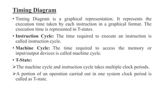
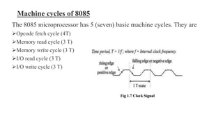
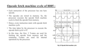
Microprocessor and
Microcontroller
Prof. P. V. Gaikwad
Lecture 1: 03/08/2023
Introduction
Basic Concepts of Microprocessor
Definition of the Microprocessor
Microprocessor Based System with Bus
Architecture
Arithmetic and Logic Unit (ALU):
ALU performs arithmetic and logical operations such as addition, subtraction, AND, OR etc and
results are stored in the register or in the memory unit or send to output unit.
Register Unit
Microprocessor consists of various registers. The registers are used for temporary storage of data
during execution of program. Some of the registers accessible to user through various instruction.
Control Unit
The control unit provides necessary timing and control signals to all the operations in the
microprocessor and peripherals including memory.
Memory
It stores binary information such as instructions and data and provide that information to
microprocessor when required
System Bus
The system bus is a communication path between the microprocessor and the peripherals. It is
nothing but a group of wires that carries data in the form of bits.
How does a microprocessor works?
Machine Language
8085 Assembly Language
Lecture 2 : 04/08/2023
Features of microprocessor 8085
Internal Architecture of 8085
Week 2
Lecture 3: 08/08/2023
Special Purpose Registers
Animation
Week 2
Lecture 4: 10/08/2023
Pin Configuration of 8085
8-bit general purpose μp
Capable of addressing 64 k of memory
Has 40 pins
Requires +5 v power supply
Can operate with 3 MHz clock
Pin configuration of 8085
All the signals can be classified into
Six groups –
1. Address Bus
2. Data Bus
3. Control & Status signals
4. Power signal & frequency
signals
5. Externally initiated signals
6. Serial I/O ports
Address & data bus
• 8085 μp consists of 16 signal pins use as address bus.
• Divide into 2 part: A15 – A8 (upper)
AD7 – AD0 (lower).
• A15 – A8 : Unidirectional, known as ‘high order address’.
• AD7 – AD0 : bidirectional and dual purpose (address and data placed
once at a time).
• AD7 – AD0 also known as ‘low order address’.
• To execute an instruction, at early stage AD7 – AD0 uses as address
bus and alternately as data bus for the next cycle.
• The method to change from address bus to data bus known as ‘bus
multiplexing’.
Control & Status signals
This group of signal includes-
 Two control signals (RD’ & WR’)
 Three status signals (IO/M’ , S1 & S0)
 One special signal (ALE)
• RD’ – Read (active low). To indicate that the I/O or memory
selected is to be read and data are available on the bus.
• WR’ – Write (Active low). This is to indicate that the data available
on the bus are to be written to memory or I/O ports.
• IO/M’ – To differentiate I/O operation or memory operations.
• ‘0’ - indicates a memory operation.
• ‘1’-indicates an I/O operation.
• IO/M’ combined with RD and WR to generate I/O and memory control
signals.
Control and Status Signals.
•S1 and S0: Status signals, similar to IO/M, can identify various
operations as shown on the following table :
Control & Status signals
•ALE (Address Latch Enable) signal :
ALE used to de-multiplex address/data bus
Active high signal - generated to show the start of 8085 operation.
ALE = 1 when AD0 –AD7 lines have an address.
ALE = 0 when AD0 – AD7 lines have a data.
Power signal & frequency signals
 Vcc : +5 V power supply
 Vss : Ground reference
 X1 & X2 : A crystal is connected at
these two pins. The frequency is
divided by two.
Therefore, to operate a system at 3
MHz, the crystal should have a
frequency of 6 MHz.
 CLK OUT : This signal is used as the
system clock for other devices.
Externally initiated Signals including Interrupt
• An interrupt is a hardware-initiated subroutine CALL.
• When interrupt pin is activated, an ISR will be called,
interrupting the program that is currently executing.
Pin Subroutine Location
TRAP 0024
RST 5.5 002C
RST 6.5 0034
RST 7.5 003C
INTR *
Note: * the address of the ISR is determined by the external hardware.
Externally initiated Signals including Interrupt
• INTR input is enabled when EI instruction is executed.
• The status of the RST 7.5, RST 6.5 and RST 5.5 pins are
determined by both EI instruction and the condition
of the mask bits in the interrupt mask register.
Externally initiated Signals including Interrupt
RESET IN’ : When the signal on this pin goes low,
the program counter is set to zero.
the buses are tri-sated.
MPU is reset.
RESET OUT : This signal is used to reset other
devices.
Serial I/O ports
The 8085 has two signals to implement the
serial transmission:
 SID: Serial Input Data
 SOD: Serial Output Data
Week 3
Lecture: 17/08/2023
Limitations of 8085
• The low order address bus is multiplexed with the data
bus. The buses need to be de-multiplexed.
• Appropriate control signals need to be generated to
interface memory and I/O with the 8085.
Generating Control Signals
De-multiplexing Address/Data Lines
De-multiplexed Address & Data bus with Control Signals
MPU Communication
Figure : Moving data form memory to MPU using instruction MOV C, A
(code machine 4FH = 0100 1111)
Instruction and data formats:
• The format of a typical instruction is composed of two parts: an
operation code or op-code and an operand.
• Every instruction needs an op-code to specify what the
operation of the instruction is and then an operand that gives
the appropriate data needed for that particular operation code.
• According to the word or byte size the 8085 instructions are
classified into three types. They are
a) One byte (single) instructions.
b) Two byte instructions.
c) Three byte instructions.
One–byte instructions: An instruction with only opcode and do not require
any data or address is called a one byte instruction.
Ex: 1. MOV C, A Hex code = 4FH (one byte)
2. ADD B Hex code = 80H (one byte)
3. CMA Hex code = 2FH (one byte)
Two–byte instructions: A two byte instruction is one which contains an 8-bit
op-code and 8-bit operand (Data).
Ex: 1. MVI A, 09 Hex code = 3E, 09 (two bytes)
2. ADD B, 07 Hex code = 80, 07 (two bytes)
3. SUB A, 05 Hex code = 97, 05 (two bytes)
Three–byte instructions: A three byte instruction contains an opcode plus a
16 – bit address.
Ex: 1.LXI H, 8509 Hex code = 21, 09, 85 (Three bytes)
2.LDA 8509 Hex code = 3A, 09, 85 (Three bytes)
3. JMP 9567 Hex code = C3, 67, 95 (Three bytes)
4. STA 3525 Hex code = 32, 35, 25 (Three bytes)
Instruction Set of 8085
An instruction is a binary pattern designed inside a microprocessor to
perform a specific function.
The entire group of instructions that a microprocessor supports is
called Instruction Set.
8085 has 246 instructions.
Each instruction is represented by an 8-bit binary value
These 8-bits of binary value is called Op-Code or Instruction Byte.
Week 3
Lecture: 18/08/2023
Addressing Modes of 8085
The various ways of specifying data are called addressing modes.
The various addressing modes of 8085 are as below:
1. Immediate addressing mode
2. Direct addressing mode
3. Register addressing mode
4. Register indirect addressing mode
5. Inherent addressing mode
Immediate addressing mode
• In immediate addressing mode the source operand is always
data.
• If the data is 8-bit, then the instruction will be of 2 bytes, if the
data is of 16-bit then the instruction will be of 3 bytes.
• MVI is the operation.
• 05 H is the immediate data (source).
• A is the destination.
Direct addressing mode
• In direct addressing mode, the data to be operated is available
inside a memory location and that memory location is directly
specified as an operand.
• The operand is directly available in the instruction itself.
• LDA is the operation.
• 2500 H is the address of source.
• Accumulator is the destination.
Register addressing mode
• In register addressing mode, the data to be operated is available
inside the register(s) and register(s) is(are) operands.
• Therefore the operation is performed within various registers of
the microprocessor.
• MOV is the operation.
• B is the source of data.
• A is the destination.
Register indirect addressing mode
• In register indirect addressing mode, the data to be operated is
available inside a memory location and that memory location is
indirectly specified by a register pair.
• MOV is the operation.
• M is the memory location specified by H-L register pair.
• A is the destination.
Inherent addressing mode
• In implied/implicit addressing mode the operand is hidden and
the data to be operated is available in the instruction itself.
• CMA is the operation.
• A is the source.
• A is the destination.
Week 4
Lecture: 22/08/2023
Classification of Instruction Set
Data Transfer Instruction
Arithmetic Instructions
Logical Instructions
Branching Instructions
Control Instructions
Data Transfer Instructions
• These instructions move data between registers, or between memory
and registers.
• These instructions copy data from source to destination.
• While copying, the contents of source are not modified.
Week 4
Lecture: 24/08/2023
Data Transfer Instruction
Opcode Operand Discription
SPHL None Copy H and L registers to stack pointer
Opcode Operand Discription
PCHL None Copy H and L registers to program counter
Arithmetic Instructions
These instructions perform the operations like:
Addition
Subtract
Increment
Decrement
Week 4
Lecture: 25/08/2023
Week 5
Lecture: 29/08/2023
Week 5
Lecture: 31/08/2023
Week 5
Lecture: 01/09/2023
Week 6
Lecture: 05/09/2023
Stack in 8085 Microprocessor
• The stack is a special area in memory used by the CPU to store register
information or general data information during program execution. The stack has
a top and a bottom.
• A stack is a region of memory that is used to store data temporarily. In the 8085
microprocessor, the stack is implemented using a dedicated block of memory
known as the stack pointer (SP).
• The memory location where a word was most recently stored is called the top of
stack.
• The stack pointer points to the current top of the stack, which is the location
where the next item will be stored.
• The stack used is a Last in first out (LIFO) structure that uses push and pull (pop)
operations.
• When data is pushed onto the stack, the stack pointer is decremented by one to
point to the next available memory location. When data is popped from the
stack, the stack pointer is incremented by one to point to the next item on the
stack.
Stack in 8085 Microprocessor
Stack Pointer Instructions
The 8085 microprocessor provides a set of instructions that can be used to
manipulate the stack. These instructions include:
1. PUSH: This instruction is used to push a register or memory location onto the stack. The contents
of the register or memory location are first copied to the memory location pointed to by the
stack pointer, and then the stack pointer is decremented.
2. POP: This instruction is used to pop the topmost item from the stack. The contents of the
memory location pointed to by the stack pointer are first copied to the register or memory
location specified in the instruction, and then the stack pointer is incremented.
PUSH rp/PSW
• This instruction is used to push a register or memory location onto the stack.
• The contents of the register or memory location are first copied to the memory
location pointed to by the stack pointer, and then the stack pointer is
decremented.
Example: PUSH B Assumes that the SP register contains 2099H, B = 32H and C =
57H
POP rp/PSW
• This instruction is used to pop the topmost item from the stack.
• The contents of the memory location pointed to by the stack pointer
are first copied to the register or memory location specified in the
instruction, and then the stack pointer is incremented.
• Example POP H
Week 6
Lecture: 08/09/2023
Timing Diagram
• Timing Diagram is a graphical representation. It represents the
execution time taken by each instruction in a graphical format. The
execution time is represented in T-states.
• Instruction Cycle: The time required to execute an instruction is
called instruction cycle.
• Machine Cycle: The time required to access the memory or
input/output devices is called machine cycle.
• T-State:
The machine cycle and instruction cycle takes multiple clock periods.
A portion of an operation carried out in one system clock period is
called as T-state.
Machine cycles of 8085
The 8085 microprocessor has 5 (seven) basic machine cycles. They are
Opcode fetch cycle (4T)
Memory read cycle (3 T)
Memory write cycle (3 T)
I/O read cycle (3 T)
I/O write cycle (3 T)
Opcode fetch machine cycle of 8085 :
• Each instruction of the processor has one byte
opcode.
• The opcodes are stored in memory. So, the
processor executes the opcode fetch machine
cycle to fetch the opcode from memory.
• Hence, every instruction starts with opcode fetch
machine cycle.
• The time taken by the processor to execute the
opcode fetch cycle is 4T.
• In this time, the first, 3 T-states are used for
fetching the opcode from memory and the
remaining T-states are used for internal
operations by the processor.

Microprocessor and Microcontroller.pptx

  • 1.
  • 2.
  • 3.
  • 4.
    Basic Concepts ofMicroprocessor
  • 5.
    Definition of theMicroprocessor
  • 6.
    Microprocessor Based Systemwith Bus Architecture
  • 7.
    Arithmetic and LogicUnit (ALU): ALU performs arithmetic and logical operations such as addition, subtraction, AND, OR etc and results are stored in the register or in the memory unit or send to output unit. Register Unit Microprocessor consists of various registers. The registers are used for temporary storage of data during execution of program. Some of the registers accessible to user through various instruction. Control Unit The control unit provides necessary timing and control signals to all the operations in the microprocessor and peripherals including memory. Memory It stores binary information such as instructions and data and provide that information to microprocessor when required System Bus The system bus is a communication path between the microprocessor and the peripherals. It is nothing but a group of wires that carries data in the form of bits.
  • 8.
    How does amicroprocessor works?
  • 9.
  • 10.
  • 11.
    Lecture 2 :04/08/2023
  • 12.
  • 13.
  • 19.
  • 20.
  • 26.
  • 27.
  • 28.
    Pin Configuration of8085 8-bit general purpose μp Capable of addressing 64 k of memory Has 40 pins Requires +5 v power supply Can operate with 3 MHz clock
  • 29.
    Pin configuration of8085 All the signals can be classified into Six groups – 1. Address Bus 2. Data Bus 3. Control & Status signals 4. Power signal & frequency signals 5. Externally initiated signals 6. Serial I/O ports
  • 30.
    Address & databus • 8085 μp consists of 16 signal pins use as address bus. • Divide into 2 part: A15 – A8 (upper) AD7 – AD0 (lower). • A15 – A8 : Unidirectional, known as ‘high order address’. • AD7 – AD0 : bidirectional and dual purpose (address and data placed once at a time). • AD7 – AD0 also known as ‘low order address’. • To execute an instruction, at early stage AD7 – AD0 uses as address bus and alternately as data bus for the next cycle. • The method to change from address bus to data bus known as ‘bus multiplexing’.
  • 31.
    Control & Statussignals This group of signal includes-  Two control signals (RD’ & WR’)  Three status signals (IO/M’ , S1 & S0)  One special signal (ALE) • RD’ – Read (active low). To indicate that the I/O or memory selected is to be read and data are available on the bus. • WR’ – Write (Active low). This is to indicate that the data available on the bus are to be written to memory or I/O ports. • IO/M’ – To differentiate I/O operation or memory operations. • ‘0’ - indicates a memory operation. • ‘1’-indicates an I/O operation. • IO/M’ combined with RD and WR to generate I/O and memory control signals.
  • 32.
    Control and StatusSignals. •S1 and S0: Status signals, similar to IO/M, can identify various operations as shown on the following table :
  • 33.
    Control & Statussignals •ALE (Address Latch Enable) signal : ALE used to de-multiplex address/data bus Active high signal - generated to show the start of 8085 operation. ALE = 1 when AD0 –AD7 lines have an address. ALE = 0 when AD0 – AD7 lines have a data.
  • 34.
    Power signal &frequency signals  Vcc : +5 V power supply  Vss : Ground reference  X1 & X2 : A crystal is connected at these two pins. The frequency is divided by two. Therefore, to operate a system at 3 MHz, the crystal should have a frequency of 6 MHz.  CLK OUT : This signal is used as the system clock for other devices.
  • 35.
    Externally initiated Signalsincluding Interrupt
  • 36.
    Externally initiated Signalsincluding Interrupt • An interrupt is a hardware-initiated subroutine CALL. • When interrupt pin is activated, an ISR will be called, interrupting the program that is currently executing. Pin Subroutine Location TRAP 0024 RST 5.5 002C RST 6.5 0034 RST 7.5 003C INTR * Note: * the address of the ISR is determined by the external hardware.
  • 37.
    Externally initiated Signalsincluding Interrupt • INTR input is enabled when EI instruction is executed. • The status of the RST 7.5, RST 6.5 and RST 5.5 pins are determined by both EI instruction and the condition of the mask bits in the interrupt mask register.
  • 38.
    Externally initiated Signalsincluding Interrupt RESET IN’ : When the signal on this pin goes low, the program counter is set to zero. the buses are tri-sated. MPU is reset. RESET OUT : This signal is used to reset other devices.
  • 39.
    Serial I/O ports The8085 has two signals to implement the serial transmission:  SID: Serial Input Data  SOD: Serial Output Data
  • 40.
  • 41.
    Limitations of 8085 •The low order address bus is multiplexed with the data bus. The buses need to be de-multiplexed. • Appropriate control signals need to be generated to interface memory and I/O with the 8085.
  • 42.
  • 43.
  • 44.
    De-multiplexed Address &Data bus with Control Signals
  • 45.
    MPU Communication Figure :Moving data form memory to MPU using instruction MOV C, A (code machine 4FH = 0100 1111)
  • 46.
    Instruction and dataformats: • The format of a typical instruction is composed of two parts: an operation code or op-code and an operand. • Every instruction needs an op-code to specify what the operation of the instruction is and then an operand that gives the appropriate data needed for that particular operation code. • According to the word or byte size the 8085 instructions are classified into three types. They are a) One byte (single) instructions. b) Two byte instructions. c) Three byte instructions.
  • 47.
    One–byte instructions: Aninstruction with only opcode and do not require any data or address is called a one byte instruction. Ex: 1. MOV C, A Hex code = 4FH (one byte) 2. ADD B Hex code = 80H (one byte) 3. CMA Hex code = 2FH (one byte) Two–byte instructions: A two byte instruction is one which contains an 8-bit op-code and 8-bit operand (Data). Ex: 1. MVI A, 09 Hex code = 3E, 09 (two bytes) 2. ADD B, 07 Hex code = 80, 07 (two bytes) 3. SUB A, 05 Hex code = 97, 05 (two bytes) Three–byte instructions: A three byte instruction contains an opcode plus a 16 – bit address. Ex: 1.LXI H, 8509 Hex code = 21, 09, 85 (Three bytes) 2.LDA 8509 Hex code = 3A, 09, 85 (Three bytes) 3. JMP 9567 Hex code = C3, 67, 95 (Three bytes) 4. STA 3525 Hex code = 32, 35, 25 (Three bytes)
  • 48.
    Instruction Set of8085 An instruction is a binary pattern designed inside a microprocessor to perform a specific function. The entire group of instructions that a microprocessor supports is called Instruction Set. 8085 has 246 instructions. Each instruction is represented by an 8-bit binary value These 8-bits of binary value is called Op-Code or Instruction Byte.
  • 49.
  • 50.
    Addressing Modes of8085 The various ways of specifying data are called addressing modes. The various addressing modes of 8085 are as below: 1. Immediate addressing mode 2. Direct addressing mode 3. Register addressing mode 4. Register indirect addressing mode 5. Inherent addressing mode
  • 51.
    Immediate addressing mode •In immediate addressing mode the source operand is always data. • If the data is 8-bit, then the instruction will be of 2 bytes, if the data is of 16-bit then the instruction will be of 3 bytes. • MVI is the operation. • 05 H is the immediate data (source). • A is the destination.
  • 52.
    Direct addressing mode •In direct addressing mode, the data to be operated is available inside a memory location and that memory location is directly specified as an operand. • The operand is directly available in the instruction itself. • LDA is the operation. • 2500 H is the address of source. • Accumulator is the destination.
  • 53.
    Register addressing mode •In register addressing mode, the data to be operated is available inside the register(s) and register(s) is(are) operands. • Therefore the operation is performed within various registers of the microprocessor. • MOV is the operation. • B is the source of data. • A is the destination.
  • 54.
    Register indirect addressingmode • In register indirect addressing mode, the data to be operated is available inside a memory location and that memory location is indirectly specified by a register pair. • MOV is the operation. • M is the memory location specified by H-L register pair. • A is the destination.
  • 55.
    Inherent addressing mode •In implied/implicit addressing mode the operand is hidden and the data to be operated is available in the instruction itself. • CMA is the operation. • A is the source. • A is the destination.
  • 56.
  • 57.
    Classification of InstructionSet Data Transfer Instruction Arithmetic Instructions Logical Instructions Branching Instructions Control Instructions
  • 58.
    Data Transfer Instructions •These instructions move data between registers, or between memory and registers. • These instructions copy data from source to destination. • While copying, the contents of source are not modified.
  • 64.
  • 70.
    Data Transfer Instruction OpcodeOperand Discription SPHL None Copy H and L registers to stack pointer Opcode Operand Discription PCHL None Copy H and L registers to program counter
  • 71.
    Arithmetic Instructions These instructionsperform the operations like: Addition Subtract Increment Decrement
  • 76.
  • 83.
  • 101.
  • 112.
  • 123.
  • 135.
    Stack in 8085Microprocessor • The stack is a special area in memory used by the CPU to store register information or general data information during program execution. The stack has a top and a bottom. • A stack is a region of memory that is used to store data temporarily. In the 8085 microprocessor, the stack is implemented using a dedicated block of memory known as the stack pointer (SP). • The memory location where a word was most recently stored is called the top of stack. • The stack pointer points to the current top of the stack, which is the location where the next item will be stored. • The stack used is a Last in first out (LIFO) structure that uses push and pull (pop) operations. • When data is pushed onto the stack, the stack pointer is decremented by one to point to the next available memory location. When data is popped from the stack, the stack pointer is incremented by one to point to the next item on the stack.
  • 136.
    Stack in 8085Microprocessor
  • 137.
    Stack Pointer Instructions The8085 microprocessor provides a set of instructions that can be used to manipulate the stack. These instructions include: 1. PUSH: This instruction is used to push a register or memory location onto the stack. The contents of the register or memory location are first copied to the memory location pointed to by the stack pointer, and then the stack pointer is decremented. 2. POP: This instruction is used to pop the topmost item from the stack. The contents of the memory location pointed to by the stack pointer are first copied to the register or memory location specified in the instruction, and then the stack pointer is incremented.
  • 138.
    PUSH rp/PSW • Thisinstruction is used to push a register or memory location onto the stack. • The contents of the register or memory location are first copied to the memory location pointed to by the stack pointer, and then the stack pointer is decremented. Example: PUSH B Assumes that the SP register contains 2099H, B = 32H and C = 57H
  • 139.
    POP rp/PSW • Thisinstruction is used to pop the topmost item from the stack. • The contents of the memory location pointed to by the stack pointer are first copied to the register or memory location specified in the instruction, and then the stack pointer is incremented. • Example POP H
  • 140.
  • 141.
    Timing Diagram • TimingDiagram is a graphical representation. It represents the execution time taken by each instruction in a graphical format. The execution time is represented in T-states. • Instruction Cycle: The time required to execute an instruction is called instruction cycle. • Machine Cycle: The time required to access the memory or input/output devices is called machine cycle. • T-State: The machine cycle and instruction cycle takes multiple clock periods. A portion of an operation carried out in one system clock period is called as T-state.
  • 142.
    Machine cycles of8085 The 8085 microprocessor has 5 (seven) basic machine cycles. They are Opcode fetch cycle (4T) Memory read cycle (3 T) Memory write cycle (3 T) I/O read cycle (3 T) I/O write cycle (3 T)
  • 143.
    Opcode fetch machinecycle of 8085 : • Each instruction of the processor has one byte opcode. • The opcodes are stored in memory. So, the processor executes the opcode fetch machine cycle to fetch the opcode from memory. • Hence, every instruction starts with opcode fetch machine cycle. • The time taken by the processor to execute the opcode fetch cycle is 4T. • In this time, the first, 3 T-states are used for fetching the opcode from memory and the remaining T-states are used for internal operations by the processor.