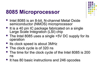
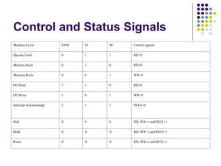
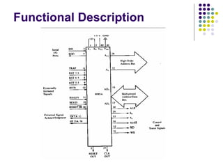
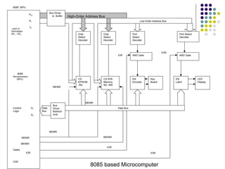
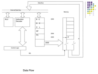
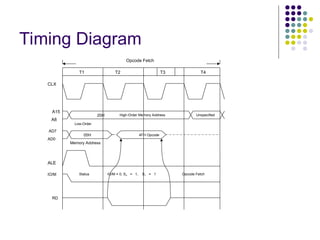
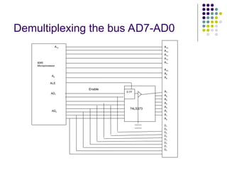
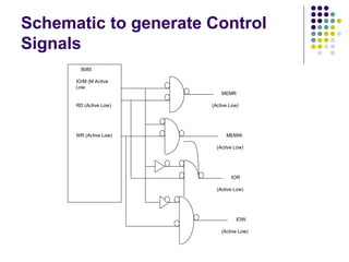
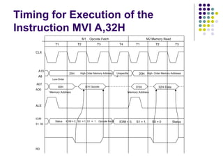
Introduction to 8085
Microprocessor
.
Digital Computer
 A digital computer is a programmable
machine specially designed for making
computation
 Its main components are
 CPU (Central Processing Unit)
 Memory
 Input device
 Output device
CPU
 The major sections of a CPU
 Arithmetic and Logic Unit (ALU)
 Accumulator
 General and Special purpose registers
 Timing and Control Unit
CPU
 The function of an ALU is to perform arithmetic
operations such as addition and subtraction; and
logical operations such as AND, OR and
EXCLUSIVE-OR
 Timing and control unit controls the entire
operations of a computer
 The accumulator is a register, which contains one of
the operands and stores results of most arithmetic
and logical operations
 General purpose registers are used for temporary
storage of data and intermediate results while
computer is making execution of a program
 Special purpose registers are used by the
microprocessor itself
Memory & I/O
 The memory is a storage device. It stores
program, data, results etc
 The computer receives data and instructions
through input devices
 The computer sends results to output devices
Microprocessor
 With the advent of LSI and VLSI technology it
became possible to build the entire CPU on a
single chip IC
 A CPU built into a single LSI/VLSI chip is
called a microprocessor
 A digital computer using microprocessor as
its CPU is called a microcomputer
Microprocessor
 The term micro initiates its physical size; not
it’s computing power
 Today the computing power of a powerful
microprocessor approaches that a CPU on
earlier large computer
 The main sections of a microprocessor are:
ALU, timing and control unit, accumulator,
general purpose and special purpose
registers
8085 Microprocessor
 Intel 8085 is an 8-bit, N-channel Metal Oxide
semiconductor (NMOS) microprocessor
 It is a 40 pin IC package fabricated on a single
Large Scale Integration (LSI) chip
 The Intel 8085 uses a single +5V DC supply for its
operation
 Its clock speed is about 3MHz
 The clock cycle is of 320 ns
 The time for the clock cycle of the Intel 8085 is 200
ns
 It has 80 basic instructions and 246 opcodes
8085 Architecture
ALU
 The ALU performs the following arithmetic and
logical operations.
 Addition
 Subtraction
 Logical AND
 Logical OR
 Logical EXCLUSIVE OR
 Complement (logical NOT)
 Increment (add 1)
 Decrement (subtract 1)
 Left shift
 Clear
Register Set
General Registers
 The 8085 has six general-purpose registers to store
8-bit data; these are identified as B, C, D, E, H, and
L
 They can be combined as register pairs - BC, DE,
and HL - to perform some 16-bit operations
 The programmer can use these registers to store or
copy data into the registers by using data copy
instructions
 The HL register pair is also used to address memory
locations
 In other words, HL register pair plays the role of
memory address register
Accumulator & Pointers
 The accumulator is an 8-bit register that is a
part of arithmetic/logic unit (ALU)
 Program Counter - Deals with sequencing
the execution of instructions. Acts as a
memory pointer
 Stack Pointer – Points to a memory location
in R/W memory, called the stack
Instruction Register/Decoder
 The instruction register and the decoder are
considered as a part of the ALU
 The instruction register is a temporary
storage for the current instruction of a
program
 The decoder decodes the instruction and
establishes the sequence of events to follow
Flags
 The ALU includes five flip-flops, which are set
or reset after an operation according to data
conditions of the result in the accumulator
and other registers
 They are called Zero (Z), Carry (CY), Sign
(S), Parity (P), and Auxiliary Carry (AC) flags
Flags
 If the sum in the accumulator id larger than
eight bits, the flip-flop uses to indicate a carry
-- called the Carry flag (CY) – is set to one
 When an arithmetic operation results in zero,
the flip-flop called the Zero (Z) flag is set to
one
Flags
 These flags have critical importance in the decision-
making process of the microprocessor
 The conditions (set or reset) of the flags are tested
through the software instructions
 The thorough understanding of flag is essential in
writing assembly language programs
 The combination of the flag register and the
accumulator is called Program Status Word (PSW)
and PSW is the 16-bit unit for stack operation
Flags
Pin Diagram
Address & Data Bus
 Address Bus
 The 8085 has eight signal lines, A15-A8,
which are unidirectional and used as the high
order address bus
 Multiplexed Address/Data Bus
 The signal lines AD7-AD0 are bidirectional
 They serve a dual purpose
Address & Data Bus
 They are used as the low-order address bus as well
as the data bus
 In executing an instruction, during the earlier part of
the cycle, these lines are used as the low-order
address bus as well as the data bus
 During the later part of the cycle, these lines are
used as the data bus
 However the low order address bus can be
separated from these signals by using a latch
Control and Status Signals
Machine Cycle IO/M S1 S0 Control signals
Opcode Fetch 0 1 1 RD=0
Memory Read 0 1 0 RD=0
Memory Write 0 0 1 WR=0
I/O Read 1 1 0 RD=0
I/O Write 1 0 1 WR=0
Interrupt Acknowledge 1 1 1 INTA=0
Halt Z 0 0 RD, WR=z and INTA=1
Hold Z X X RD, WR=z and INTA=1
Reset Z X X RD, WR=z and INTA=1
Functional Description
Bus Driver
or Buffer
Bus
Driver
Bidirecti
onal
Chip
Select
Decoder
Chip
Select
Decoder
Port
Select
Decoder
Port Select
Decoder
CS
EPROM
RD
CS R/W
Memory
RD WR
EN
Encoder
Key
Board
EN
Latch
LED
Display
AND Gate
Data
Bus
AND Gate
IOR
IOW
High-Order Address Bus
8085 MPU
A15
A7
A0
D7
D0
MEMR
MEMW
Gates
IOR
IOW
8085
Microprocessor
(MPU)
Control
Logic
Latch to
Demultiplex
AD7 – AD0
Low-Order Address Bus
Data Bus
MEMR
MEMW
IOR
IOW
MEMR
MEMR
8085 based Microcomputer
ALU Instruction
Decoder
B C
D E
H L
SP
PC
Control Logic
2005
Data Bus
Internal Data Bus
Memory
RD
4F
4F
2000
2004
2005
Data Flow
Timing Diagram
T1 T2 T3 T4
CLX
Opcode Fetch
A15
A8
AD7
AD0
ALE
IO/M
RD
20H High-Order Memory Address Unspecified
Low-Order
05H 4FH Opcode
Memory Address
Status IO/M = 0, S0 = 1, S1 = 1 Opcode Fetch
Demultiplexing the bus AD7-AD0
8085
Microprocessor
A8
ALE
AD7
AD0
A15 A15
A14
A13
A12
A11
A10
A9
A8
A7
A6
A5
A4
A3
A2
A1
A0
D7
D6
D5
D4
D3
D2
D1
D0
Enable
74LS373
D FF
Schematic to generate Control
Signals
8085
IO/M (M Active
Low
RD (Active Low)
WR (Active Low)
MEMR
MEMW
IOR
IOW
(Active Low)
(Active Low)
(Active Low)
(Active Low)
Timing for Execution of the
Instruction MVI A,32H
T1 T2 T3 T4
CLX
M1 Opcode Fetch
A15
A8
AD7
AD0
ALE
IO/M
RD
20H High-Order Memory Address Unspecifie
d
Low-Order
00H 3EH Opcode
Memory Address
Status IO/M = 0, S0 = 1, S1 = 1 Opcode Fetch
S1, S0
M2 Memory Read
T1 T2 T3
20H High- Order Memory Addresss
01H 32H Data
Memory Address
IO/M = 0, S1 = 1, S0 = 0 Status
Addressing Modes
 Various ways of specifying the operands or various
formats for specifying the operands is called
addressing mode
 8-bit or 16-bit data may be directly given in the
instruction itself
 The address of the memory location, I/O port or I/O
device, where data resides, may be given in the
instruction itself
 In some instructions only one register is specified.
The content of the specified register is one of the
operands. It is understood that the other operand is
in the accumulator.
Addressing Modes
 Some instructions specify one or two
registers. The contents of the registers are
the required data.
 In some instructions data is implied. The
most instructions of this type operate on the
content of the accumulator.
Addressing Modes
 Implicit addressing
 CMA – Complement the contents of accumulator
 Immediate addressing
 MVI R, 05H
 ADI 06H
 Direct addressing – The address of the
operand in the instruction - STA 2400H, IN
02H
Addressing Modes
 Register addressing
 In register addressing mode the operands are in
the general purpose registers
 MOV A, B
 ADD B
 Register indirect addressing
 Memory location is specified by the contents of
the registers
 LDAX B, STAX D
Data Transfer Instructions
Types Examples
1. Between Registers 1. MOV B,D – Copy the contents of the
register B into Register D
2. Specific data byte to a register or a
memory location
2. MVI B,32H – Load register B with the
data byte 32H
3. Between a memory location and a
register
3. LXI H, 2000H
MOV B,M
From a memory location 2000H to register
B
4. Between an I/O device and the
accumulator
4. IN 05H – The contents of the input port
designated in the operand are read and
loaded into the accumulator
Arithmetic Instructions
 ADD B – [A] <----- [A]+[B]
 ADD M - [A] <----- [A]+[[HL]]
 DAD B – [HL] <----- [HL]+[BC]
 SUB C – [A] <----- [A]+[C]
 SUI 76H – [A] <---- [A]-76H
 SBB M – [A] <----- [A]-[[HL]]-[C]
Logical Instructions
 ANA C – [A] <----- [A] ^ [C]
 ANI 85H – [A] <----- [A] ^ 85H
 ORA M – [A] <----- [A] v [[HL]]
 XRA B – [A] <------ [A] XOR [B]
Rotate Instructions
 RLC
 [An+1] <----- [An]
 [A0] <------ [A7]
 [CS] <----- [A7]
 RAR
 [An] <------ [An+1]
 [CS] <------ [A0]
 [A7] <------ [CS]
Complement Instructions
 CMP R
 CPI data
Complement Instructions
 CMA – [A] <---- [A]’
 CMC – [CS] <----- [CS]’
Transfer Instructions
 JMP 2050H – [PC] <----- 2050H
 JZ 3100H – [PC] <----- 3100H if Z=1,
otherwise [PC] <----- [PC]+1
 JNC 4250H – [PC] <----- 4250H if
C=0, otherwise [PC] <----- [PC]+1
CALL & RET
 CALL Addr
 [[SP]-1] <------- [PCH]
 [[SP]-1] <------- [PCL]
 [SP] <----- [SP]-2
 [PC] <----- Addr
 RET
 [PCL] <------ [[SP]]
 [PCH] <------ [[SP]+1]
 [SP] <------ [SP]+2
One Byte Instructions
Two Byte Instructions
Writing Assembly Language
Program
 Define the problem clearly and make the problem
statement.
 Analyze the problem thoroughly. In this step we
divide the problem into smaller steps to examine
the process of writing programs.
 Draw the flow chart. The steps listed in the
problem analysis and the sequences are
represented in a block diagram.
 Translate the blocks shown in the flowchart into
8085 operations and then subsequently into
mnemonics.
Conversion and Execution
 Convert the mnemonics into Hex code; we
need to look up the code in 8085 instruction
set.
 Store the program in Read/Write memory of a
single-board microcomputer. This may
require the knowledge about memory
addresses and the output port addresses.
 Finally execute the program.
DMA
 Device wishing to perform DMA asserts the
processors bus request signal.
 Processor completes the current bus cycle and
then asserts the bus grant signal to the device.
 The device then asserts the bus grant ack signal.
 The processor senses in the change in the state of
bus grant ack signal and starts listening to the
data and address bus for DMA activity.
DMA
 The DMA device performs the transfer from the
source to destination address.
 During these transfers, the processor monitors the
addresses on the bus and checks if any location
modified during DMA operations is cached in the
processor. If the processor detects a cached
address on the bus, it can take one of the two
actions:
 Processor invalidates the internal cache entry for the
address involved in DMA write operation
 Processor updates the internal cache when a DMA write is
detected
DMA
 Once the DMA operations have been
completed, the device releases the bus by
asserting the bus release signal.
 Processor acknowledges the bus release and
resumes its bus cycles from the point it left
off.

8085 Microprocessor artchitecture -ppt.ppt

  • 1.
  • 2.
    Digital Computer  Adigital computer is a programmable machine specially designed for making computation  Its main components are  CPU (Central Processing Unit)  Memory  Input device  Output device
  • 3.
    CPU  The majorsections of a CPU  Arithmetic and Logic Unit (ALU)  Accumulator  General and Special purpose registers  Timing and Control Unit
  • 4.
    CPU  The functionof an ALU is to perform arithmetic operations such as addition and subtraction; and logical operations such as AND, OR and EXCLUSIVE-OR  Timing and control unit controls the entire operations of a computer  The accumulator is a register, which contains one of the operands and stores results of most arithmetic and logical operations  General purpose registers are used for temporary storage of data and intermediate results while computer is making execution of a program  Special purpose registers are used by the microprocessor itself
  • 5.
    Memory & I/O The memory is a storage device. It stores program, data, results etc  The computer receives data and instructions through input devices  The computer sends results to output devices
  • 6.
    Microprocessor  With theadvent of LSI and VLSI technology it became possible to build the entire CPU on a single chip IC  A CPU built into a single LSI/VLSI chip is called a microprocessor  A digital computer using microprocessor as its CPU is called a microcomputer
  • 7.
    Microprocessor  The termmicro initiates its physical size; not it’s computing power  Today the computing power of a powerful microprocessor approaches that a CPU on earlier large computer  The main sections of a microprocessor are: ALU, timing and control unit, accumulator, general purpose and special purpose registers
  • 8.
    8085 Microprocessor  Intel8085 is an 8-bit, N-channel Metal Oxide semiconductor (NMOS) microprocessor  It is a 40 pin IC package fabricated on a single Large Scale Integration (LSI) chip  The Intel 8085 uses a single +5V DC supply for its operation  Its clock speed is about 3MHz  The clock cycle is of 320 ns  The time for the clock cycle of the Intel 8085 is 200 ns  It has 80 basic instructions and 246 opcodes
  • 9.
  • 10.
    ALU  The ALUperforms the following arithmetic and logical operations.  Addition  Subtraction  Logical AND  Logical OR  Logical EXCLUSIVE OR  Complement (logical NOT)  Increment (add 1)  Decrement (subtract 1)  Left shift  Clear
  • 11.
  • 12.
    General Registers  The8085 has six general-purpose registers to store 8-bit data; these are identified as B, C, D, E, H, and L  They can be combined as register pairs - BC, DE, and HL - to perform some 16-bit operations  The programmer can use these registers to store or copy data into the registers by using data copy instructions  The HL register pair is also used to address memory locations  In other words, HL register pair plays the role of memory address register
  • 13.
    Accumulator & Pointers The accumulator is an 8-bit register that is a part of arithmetic/logic unit (ALU)  Program Counter - Deals with sequencing the execution of instructions. Acts as a memory pointer  Stack Pointer – Points to a memory location in R/W memory, called the stack
  • 14.
    Instruction Register/Decoder  Theinstruction register and the decoder are considered as a part of the ALU  The instruction register is a temporary storage for the current instruction of a program  The decoder decodes the instruction and establishes the sequence of events to follow
  • 15.
    Flags  The ALUincludes five flip-flops, which are set or reset after an operation according to data conditions of the result in the accumulator and other registers  They are called Zero (Z), Carry (CY), Sign (S), Parity (P), and Auxiliary Carry (AC) flags
  • 16.
    Flags  If thesum in the accumulator id larger than eight bits, the flip-flop uses to indicate a carry -- called the Carry flag (CY) – is set to one  When an arithmetic operation results in zero, the flip-flop called the Zero (Z) flag is set to one
  • 17.
    Flags  These flagshave critical importance in the decision- making process of the microprocessor  The conditions (set or reset) of the flags are tested through the software instructions  The thorough understanding of flag is essential in writing assembly language programs  The combination of the flag register and the accumulator is called Program Status Word (PSW) and PSW is the 16-bit unit for stack operation
  • 18.
  • 19.
  • 20.
    Address & DataBus  Address Bus  The 8085 has eight signal lines, A15-A8, which are unidirectional and used as the high order address bus  Multiplexed Address/Data Bus  The signal lines AD7-AD0 are bidirectional  They serve a dual purpose
  • 21.
    Address & DataBus  They are used as the low-order address bus as well as the data bus  In executing an instruction, during the earlier part of the cycle, these lines are used as the low-order address bus as well as the data bus  During the later part of the cycle, these lines are used as the data bus  However the low order address bus can be separated from these signals by using a latch
  • 22.
    Control and StatusSignals Machine Cycle IO/M S1 S0 Control signals Opcode Fetch 0 1 1 RD=0 Memory Read 0 1 0 RD=0 Memory Write 0 0 1 WR=0 I/O Read 1 1 0 RD=0 I/O Write 1 0 1 WR=0 Interrupt Acknowledge 1 1 1 INTA=0 Halt Z 0 0 RD, WR=z and INTA=1 Hold Z X X RD, WR=z and INTA=1 Reset Z X X RD, WR=z and INTA=1
  • 23.
  • 24.
    Bus Driver or Buffer Bus Driver Bidirecti onal Chip Select Decoder Chip Select Decoder Port Select Decoder PortSelect Decoder CS EPROM RD CS R/W Memory RD WR EN Encoder Key Board EN Latch LED Display AND Gate Data Bus AND Gate IOR IOW High-Order Address Bus 8085 MPU A15 A7 A0 D7 D0 MEMR MEMW Gates IOR IOW 8085 Microprocessor (MPU) Control Logic Latch to Demultiplex AD7 – AD0 Low-Order Address Bus Data Bus MEMR MEMW IOR IOW MEMR MEMR 8085 based Microcomputer
  • 25.
    ALU Instruction Decoder B C DE H L SP PC Control Logic 2005 Data Bus Internal Data Bus Memory RD 4F 4F 2000 2004 2005 Data Flow
  • 26.
    Timing Diagram T1 T2T3 T4 CLX Opcode Fetch A15 A8 AD7 AD0 ALE IO/M RD 20H High-Order Memory Address Unspecified Low-Order 05H 4FH Opcode Memory Address Status IO/M = 0, S0 = 1, S1 = 1 Opcode Fetch
  • 27.
    Demultiplexing the busAD7-AD0 8085 Microprocessor A8 ALE AD7 AD0 A15 A15 A14 A13 A12 A11 A10 A9 A8 A7 A6 A5 A4 A3 A2 A1 A0 D7 D6 D5 D4 D3 D2 D1 D0 Enable 74LS373 D FF
  • 28.
    Schematic to generateControl Signals 8085 IO/M (M Active Low RD (Active Low) WR (Active Low) MEMR MEMW IOR IOW (Active Low) (Active Low) (Active Low) (Active Low)
  • 29.
    Timing for Executionof the Instruction MVI A,32H T1 T2 T3 T4 CLX M1 Opcode Fetch A15 A8 AD7 AD0 ALE IO/M RD 20H High-Order Memory Address Unspecifie d Low-Order 00H 3EH Opcode Memory Address Status IO/M = 0, S0 = 1, S1 = 1 Opcode Fetch S1, S0 M2 Memory Read T1 T2 T3 20H High- Order Memory Addresss 01H 32H Data Memory Address IO/M = 0, S1 = 1, S0 = 0 Status
  • 30.
    Addressing Modes  Variousways of specifying the operands or various formats for specifying the operands is called addressing mode  8-bit or 16-bit data may be directly given in the instruction itself  The address of the memory location, I/O port or I/O device, where data resides, may be given in the instruction itself  In some instructions only one register is specified. The content of the specified register is one of the operands. It is understood that the other operand is in the accumulator.
  • 31.
    Addressing Modes  Someinstructions specify one or two registers. The contents of the registers are the required data.  In some instructions data is implied. The most instructions of this type operate on the content of the accumulator.
  • 32.
    Addressing Modes  Implicitaddressing  CMA – Complement the contents of accumulator  Immediate addressing  MVI R, 05H  ADI 06H  Direct addressing – The address of the operand in the instruction - STA 2400H, IN 02H
  • 33.
    Addressing Modes  Registeraddressing  In register addressing mode the operands are in the general purpose registers  MOV A, B  ADD B  Register indirect addressing  Memory location is specified by the contents of the registers  LDAX B, STAX D
  • 34.
    Data Transfer Instructions TypesExamples 1. Between Registers 1. MOV B,D – Copy the contents of the register B into Register D 2. Specific data byte to a register or a memory location 2. MVI B,32H – Load register B with the data byte 32H 3. Between a memory location and a register 3. LXI H, 2000H MOV B,M From a memory location 2000H to register B 4. Between an I/O device and the accumulator 4. IN 05H – The contents of the input port designated in the operand are read and loaded into the accumulator
  • 35.
    Arithmetic Instructions  ADDB – [A] <----- [A]+[B]  ADD M - [A] <----- [A]+[[HL]]  DAD B – [HL] <----- [HL]+[BC]  SUB C – [A] <----- [A]+[C]  SUI 76H – [A] <---- [A]-76H  SBB M – [A] <----- [A]-[[HL]]-[C]
  • 36.
    Logical Instructions  ANAC – [A] <----- [A] ^ [C]  ANI 85H – [A] <----- [A] ^ 85H  ORA M – [A] <----- [A] v [[HL]]  XRA B – [A] <------ [A] XOR [B]
  • 37.
    Rotate Instructions  RLC [An+1] <----- [An]  [A0] <------ [A7]  [CS] <----- [A7]  RAR  [An] <------ [An+1]  [CS] <------ [A0]  [A7] <------ [CS]
  • 38.
  • 39.
    Complement Instructions  CMA– [A] <---- [A]’  CMC – [CS] <----- [CS]’
  • 40.
    Transfer Instructions  JMP2050H – [PC] <----- 2050H  JZ 3100H – [PC] <----- 3100H if Z=1, otherwise [PC] <----- [PC]+1  JNC 4250H – [PC] <----- 4250H if C=0, otherwise [PC] <----- [PC]+1
  • 41.
    CALL & RET CALL Addr  [[SP]-1] <------- [PCH]  [[SP]-1] <------- [PCL]  [SP] <----- [SP]-2  [PC] <----- Addr  RET  [PCL] <------ [[SP]]  [PCH] <------ [[SP]+1]  [SP] <------ [SP]+2
  • 42.
  • 43.
  • 44.
    Writing Assembly Language Program Define the problem clearly and make the problem statement.  Analyze the problem thoroughly. In this step we divide the problem into smaller steps to examine the process of writing programs.  Draw the flow chart. The steps listed in the problem analysis and the sequences are represented in a block diagram.  Translate the blocks shown in the flowchart into 8085 operations and then subsequently into mnemonics.
  • 45.
    Conversion and Execution Convert the mnemonics into Hex code; we need to look up the code in 8085 instruction set.  Store the program in Read/Write memory of a single-board microcomputer. This may require the knowledge about memory addresses and the output port addresses.  Finally execute the program.
  • 46.
    DMA  Device wishingto perform DMA asserts the processors bus request signal.  Processor completes the current bus cycle and then asserts the bus grant signal to the device.  The device then asserts the bus grant ack signal.  The processor senses in the change in the state of bus grant ack signal and starts listening to the data and address bus for DMA activity.
  • 47.
    DMA  The DMAdevice performs the transfer from the source to destination address.  During these transfers, the processor monitors the addresses on the bus and checks if any location modified during DMA operations is cached in the processor. If the processor detects a cached address on the bus, it can take one of the two actions:  Processor invalidates the internal cache entry for the address involved in DMA write operation  Processor updates the internal cache when a DMA write is detected
  • 48.
    DMA  Once theDMA operations have been completed, the device releases the bus by asserting the bus release signal.  Processor acknowledges the bus release and resumes its bus cycles from the point it left off.