This document provides an overview of computer architecture and organization. It discusses the following key points in 3 or fewer sentences:
The document defines a system and describes the hardware and software components of a computer system. It then discusses different levels of design in computer architecture - the gate level, register level, and processor level. Finally, it provides examples of common components used at the register level like multiplexers, decoders, registers, and counters.
The critical routines within signal processing algorithms are typically data intensive and iterate many times, carrying out the same functions on multi-dimensional arrays and input streams. These routines use the vast majority of an implementation’s resources, and for the longest time over the course of the algorithms execution. Such routines are classed as Nested-Loop Programs. Whether the implementation is software running on a processor or a higher performance customized hardware implementation, there is always a tradeoff between the throughput performance (execution-time) and the resources used such as the amount of processor memory and registers in a software implementation or the gate-count in a hardware implementation. This article shows the reader techniques and methods for manipulating a signal processing algorithm, in particular those conforming to a Nested-Loop Program, and the different generic implementation architectures along this tradeoff spectrum, as well as the different methods for describing and analyzing an algorithm implementation. Each of these methods for describing an algorithm is shown to correspond to a different abstraction-level view and as such exposes different features and properties for ease of analysis and manipulation. Manipulation techniques, mainly algorithmic-transformations are described and it is shown how these transformations take an implementation and form a new one at a different point in the trade-off spectrum of resources used versus throughput by performing calculations in a different order and a different way to arrive at the same result.
The Easy Guide for Component Diagrams by Creately.
Creately offers wide range of Component Diagrams which can be edited instantly using our component diagram online Editor. We have listed 10 Component Diagrams here, and you can find variety of different templates on our diagram community as well. All our popular diagram templates are available for free. Just click on the "Use as Template" button to immediately start modifying it using our online diagramming tools.
Design and implementation of complex floating point processor using fpgaVLSICS Design
This paper presents complete processor hardware with three arithmetic units. The first arithmetic unit can
perform 32-bit integer arithmetic operations. The second unit can perform arithmetic operations such as
addition, subtraction, multiplication, division, and square root on 32-bit floating point numbers. The third
unit can perform arithmetic operations such as addition, subtraction, multiplication on complex numbers.
The specific advancement in this processor is the new architecture introduced for complex arithmetic unit.
In general complex floating point arithmetic hardware consists of floating to fixed and fixed to floating
conversions. But using such hardware will lead to compromise between accuracy and number of bits used
to represent the fixed point equivalent of floating point numbers. The proposed architecture avoids that
compromise and it is implemented with less number of look-up tables to save around 5500 logic gates. The
complex numbers are represented using a subset of IEEE754 standard floating point format, 16-bits for
real part and 16-bits for imaginary part. The floating point arithmetic unit works on 32-bit IEEE754 single
precision numbers. The instruction set is specially designed to support integer, floating point and complex
floating point arithmetic operations. The on-chip RAM is 8kBytes and is extendable up to 64kBytes. As the
processor is designed to implement on FPGA, the embedded block RAMs are utilized as RAM.
Download Complete Material - https://www.instamojo.com/prashanth_ns/
This Programming Using C++ contain 22 Units and each Unit contains 60 to 80 slides in it.
Course Outline...
• Introduction to Oops
• Structure of a program
• Iteration structures (loops)
• Scope of variables
• Write and execute C++ programs
• Use arrays and structures
• Pointers
• Arguments passed by value and by reference.
• Overloaded functions
• Inline functions
• Data Structures
• Unions
• Implement encapsulation and abstraction
• Use operators and decision-making constructs
• Work with arrays
• Implement polymorphism and inheritance
• Use exception handling and templates
• Implement linked lists
Data may be organized in many different ways; the logical or mathematical model of a particular organization of data is called "Data Structure". The choice of a particular data model depends on two considerations:
It must be rich enough in structure to reflect the actual relationships of the data in the real world.
The structure should be simple enough that one can effectively process the data when necessary.
Data Structure Operations
The particular data structure that one chooses for a given situation depends largely on the nature of specific operations to be performed.
The following are the four major operations associated with any data structure:
i. Traversing : Accessing each record exactly once so that certain items in the record may be processed.
ii. Searching : Finding the location of the record with a given key value, or finding the locations of all records which satisfy one or more conditions.
iii. Inserting : Adding a new record to the structure.
iv. Deleting : Removing a record from the structure.
Primitive and Composite Data Types
Primitive Data Types are Basic data types of any language. In most computers these are native to the machine's hardware.
Some Primitive data types are:
Integer
COMPUTER EDUCATION - ARCH 383
COMPUTER HARDWARES
FUNCTIONAL UNITS
PC SYSTEMATIC DECOMPOSITION
SIMPLE CONSTRUCTS
EFFECT OF COMPUTERIZATION ON ARCHITECTURE
List and describe various features of electronic systems.List and .pdfinfo824691
List and describe various features of electronic systems.
List and discuss the steps in designing an embedded system.
Solution
Electronic system level (ESL) design and verification is an emerging electronic design
methodology that focuses primarily on the higher abstraction level concerns. The termElectronic
System Level or ESL Design was first defined by Gartner Dataquest, an EDA-industry-analysis
firm, on February 1, 2001. It is defined in the ESL Design and Verification book as: \"the
utilization of appropriate abstractions in order to increase comprehension about a system, and to
enhance the probability of a successful implementation of functionality in a cost-effective
manner.\" The basic premise is to model the behavior of the entire system using a high-level
language such as C, C++, LabVIEW, or MATLAB or using graphical \"model-based\" design
tools like SystemVue, VisualSim Architect or Simulink. Newer languages are emerging that
enable the creation of a model at a higher level of abstraction including general purpose system
design languages like SysML as well as those that are specific to embedded system design like
SMDL and SSDL supported by emerging system design automation products like Teraptor.
Rapid and correct-by-construction implementation of the system can be automated using EDA
tools such as high-level synthesis and embedded softwaretools, although much of it is performed
manually today. ESL can also be accomplished through the use of SystemC as an abstract
modeling language.
Electronic System Level is now an established approach at most of the world’s leading System-
on-a-chip (SoC) design companies, and is being used increasingly in system design.[citation
needed] From its genesis as an algorithm modeling methodology with ‘no links to
implementation’, ESL is evolving into a set of complementary methodologies that enable
embedded system design, verification, and debugging through to the hardware and software
implementation of custom SoC, system-on-FPGA, system-on board, and entire multi-board
systems.
Second Part
An embedded system is one with computing hardware that has software “embedded” in it as one
of its core components. We are surrounded by embedded systems that add luxury to our lives
like mobile handsets, washing machines, microwaves, ATM machines, and air conditioners, to
name just a few. Because of certain application requirements, engineers have to approach
embedded design in a different way than other types of designs.
The following offers a brief step-by-step approach to follow while designing an embedded
system
1. Proposal: - An innovative idea or system that makes life easier and/or reduces the amount of
human effort required to complete a task.
2. Definition: - Next, the whole system needs to be designed, including what it will do under all
possible sets of input conditions. This definition is perhaps the most critical part, as any error
here will affect the working of whole system.
I. I/O Considerations: -.
Here we uploaded E workshop system design with complete details. This details helpful for students who are freshers. Even software developers can refer this document. For project source code visit www.studentprojectguide.com
Due 24 August (Friday, 1159 p.m. EDT)Use Module 1 and Book Ch.docxjacksnathalie
Due 24 August (Friday, 11:59 p.m. EDT)
Use Module 1 and Book Chapters 1 – 3 (module at bottom/chapters attached)
SHOW ALL WORK OR NO CREDIT
1. (10 Points) Virtualization is a concept that has taken on major importance in the early twenty-first century. Explain what is meant by virtualization.
2. (10 Points) What is a protocol? What is a standard? Do all protocols have to be standards? Explain.
3. (10 Points) Protocols and standards are important features of networks. Why is this so?
4. (10 Points) What are the most important ideas, keywords, and phrases that are stated in the definition of a system?
5. (10 Points) Convert the following hexadecimal numbers to decimal: .
a) 4E
b) 3D7
c) 3D70
6. (10 Points) Add the following binary numbers:
a)
101101101
+ 10011011
b)
110111111
+ 110111111
c)
1101
1010
111
+ 101
7. (10 Points) Multiply the following binary numbers together:
a)
1101
× 101
b)
11011
× 1011
8. (10 Points) Perform the following binary divisions:
a) 1010001001 ÷ 110
b) 11000000000 ÷ 1011
9. (10 Points) Using the division method, convert the following decimal numbers to binary:
a.) 4098
b) 71269
10. (10 Points) Convert the following binary numbers directly to hexadecimal: .
a) 101101110111010
b) 1111111111110001
Module 1
1. Computer Systems
We start this section with a short discussion of why you should be studying software, hardware, and data concepts. You may ask:
· Why should we study the concepts of computer data, computer hardware, and computer software?
· What are the components of a digital computer system and how do they work together?
· How are information systems developed for computers?1.1 Why Study Computer Concepts?
The answer to this question is that the understanding of these concepts is at the very foundation of being both competent and successful in your segment of the field of computers.
Computer users will:
· be aware of system capabilities, strategies, and limitations
· better understand the commands that they use
· be able to make informed decisions about computer equipment and applications
· improve their ability to communicate with other computer professionals
Computer programmers will:
· be able to write better programs by using characteristics of the computer to make the programs more efficient
· understand why compiled languages such as COBOL, C++, or Java run faster than interpreted languages such as BASIC
System analysts will be able to:
· read and understand technical specifications
· determine the correct computer strategy for a particular application
· assist management in determining computer strategy
· determine when to replace older equipment
System administrators or managers will:
· maximize the efficiency of their computer systems
· know when additional resources are required for those systems
· understand how to specify and configure operating system parameters
· know how to set up file systems
· be able to manage system and user PC upgrades
Each of these computer pro ...
FellowBuddy.com is an innovative platform that brings students together to share notes, exam papers, study guides, project reports and presentation for upcoming exams.
We connect Students who have an understanding of course material with Students who need help.
Benefits:-
# Students can catch up on notes they missed because of an absence.
# Underachievers can find peer developed notes that break down lecture and study material in a way that they can understand
# Students can earn better grades, save time and study effectively
Our Vision & Mission – Simplifying Students Life
Our Belief – “The great breakthrough in your life comes when you realize it, that you can learn anything you need to learn; to accomplish any goal that you have set for yourself. This means there are no limits on what you can be, have or do.”
Like Us - https://www.facebook.com/FellowBuddycom
Hierarchical Digital Twin of a Naval Power SystemKerry Sado
A hierarchical digital twin of a Naval DC power system has been developed and experimentally verified. Similar to other state-of-the-art digital twins, this technology creates a digital replica of the physical system executed in real-time or faster, which can modify hardware controls. However, its advantage stems from distributing computational efforts by utilizing a hierarchical structure composed of lower-level digital twin blocks and a higher-level system digital twin. Each digital twin block is associated with a physical subsystem of the hardware and communicates with a singular system digital twin, which creates a system-level response. By extracting information from each level of the hierarchy, power system controls of the hardware were reconfigured autonomously. This hierarchical digital twin development offers several advantages over other digital twins, particularly in the field of naval power systems. The hierarchical structure allows for greater computational efficiency and scalability while the ability to autonomously reconfigure hardware controls offers increased flexibility and responsiveness. The hierarchical decomposition and models utilized were well aligned with the physical twin, as indicated by the maximum deviations between the developed digital twin hierarchy and the hardware.
NO1 Uk best vashikaran specialist in delhi vashikaran baba near me online vas...Amil Baba Dawood bangali
Contact with Dawood Bhai Just call on +92322-6382012 and we'll help you. We'll solve all your problems within 12 to 24 hours and with 101% guarantee and with astrology systematic. If you want to take any personal or professional advice then also you can call us on +92322-6382012 , ONLINE LOVE PROBLEM & Other all types of Daily Life Problem's.Then CALL or WHATSAPP us on +92322-6382012 and Get all these problems solutions here by Amil Baba DAWOOD BANGALI
#vashikaranspecialist #astrologer #palmistry #amliyaat #taweez #manpasandshadi #horoscope #spiritual #lovelife #lovespell #marriagespell#aamilbabainpakistan #amilbabainkarachi #powerfullblackmagicspell #kalajadumantarspecialist #realamilbaba #AmilbabainPakistan #astrologerincanada #astrologerindubai #lovespellsmaster #kalajaduspecialist #lovespellsthatwork #aamilbabainlahore#blackmagicformarriage #aamilbaba #kalajadu #kalailam #taweez #wazifaexpert #jadumantar #vashikaranspecialist #astrologer #palmistry #amliyaat #taweez #manpasandshadi #horoscope #spiritual #lovelife #lovespell #marriagespell#aamilbabainpakistan #amilbabainkarachi #powerfullblackmagicspell #kalajadumantarspecialist #realamilbaba #AmilbabainPakistan #astrologerincanada #astrologerindubai #lovespellsmaster #kalajaduspecialist #lovespellsthatwork #aamilbabainlahore #blackmagicforlove #blackmagicformarriage #aamilbaba #kalajadu #kalailam #taweez #wazifaexpert #jadumantar #vashikaranspecialist #astrologer #palmistry #amliyaat #taweez #manpasandshadi #horoscope #spiritual #lovelife #lovespell #marriagespell#aamilbabainpakistan #amilbabainkarachi #powerfullblackmagicspell #kalajadumantarspecialist #realamilbaba #AmilbabainPakistan #astrologerincanada #astrologerindubai #lovespellsmaster #kalajaduspecialist #lovespellsthatwork #aamilbabainlahore #Amilbabainuk #amilbabainspain #amilbabaindubai #Amilbabainnorway #amilbabainkrachi #amilbabainlahore #amilbabaingujranwalan #amilbabainislamabad
Water billing management system project report.pdfKamal Acharya
Our project entitled “Water Billing Management System” aims is to generate Water bill with all the charges and penalty. Manual system that is employed is extremely laborious and quite inadequate. It only makes the process more difficult and hard.
The aim of our project is to develop a system that is meant to partially computerize the work performed in the Water Board like generating monthly Water bill, record of consuming unit of water, store record of the customer and previous unpaid record.
We used HTML/PHP as front end and MYSQL as back end for developing our project. HTML is primarily a visual design environment. We can create a android application by designing the form and that make up the user interface. Adding android application code to the form and the objects such as buttons and text boxes on them and adding any required support code in additional modular.
MySQL is free open source database that facilitates the effective management of the databases by connecting them to the software. It is a stable ,reliable and the powerful solution with the advanced features and advantages which are as follows: Data Security.MySQL is free open source database that facilitates the effective management of the databases by connecting them to the software.
6th International Conference on Machine Learning & Applications (CMLA 2024)ClaraZara1
6th International Conference on Machine Learning & Applications (CMLA 2024) will provide an excellent international forum for sharing knowledge and results in theory, methodology and applications of on Machine Learning & Applications.
ACEP Magazine edition 4th launched on 05.06.2024Rahul
This document provides information about the third edition of the magazine "Sthapatya" published by the Association of Civil Engineers (Practicing) Aurangabad. It includes messages from current and past presidents of ACEP, memories and photos from past ACEP events, information on life time achievement awards given by ACEP, and a technical article on concrete maintenance, repairs and strengthening. The document highlights activities of ACEP and provides a technical educational article for members.
We have compiled the most important slides from each speaker's presentation. This year’s compilation, available for free, captures the key insights and contributions shared during the DfMAy 2024 conference.
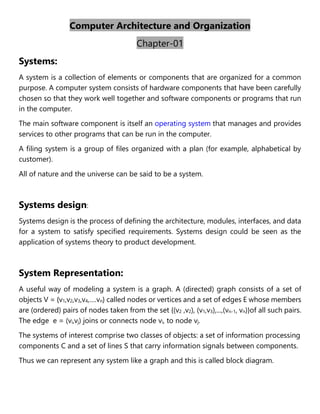
1. Computer Architecture and Organization
Chapter-01
Systems:
A system is a collection of elements or components that are organized for a common
purpose. A computer system consists of hardware components that have been carefully
chosen so that they work well together and software components or programs that run
in the computer.
The main software component is itself an operating system that manages and provides
services to other programs that can be run in the computer.
A filing system is a group of files organized with a plan (for example, alphabetical by
customer).
All of nature and the universe can be said to be a system.
Systems design:
Systems design is the process of defining the architecture, modules, interfaces, and data
for a system to satisfy specified requirements. Systems design could be seen as the
application of systems theory to product development.
System Representation:
A useful way of modeling a system is a graph. A (directed) graph consists of a set of
objects V = {v1,v2,v3,v4,….vn} called nodes or vertices and a set of edges E whose members
are (ordered) pairs of nodes taken from the set {(v2 ,v2), (v1,v3),...,(vn-1, vn)}of all such pairs.
The edge e = (vi,vj) joins or connects node vi, to node vj.
The systems of interest comprise two classes of objects: a set of information processing
components C and a set of lines S that carry information signals between components.
Thus we can represent any system like a graph and this is called block diagram.
2. Structure in Computer Architecture:
We define the structure of a system as the abstract graph consisting of its block diagram
with no functional information. A structural description merely names components and
defines their interconnection.
Behavior in Computer Architecture:
A behavioral description, enables one to determine for any given input signal a to the
system, the corresponding output f(a). We define the function f to be the behavior of the
system. The behavior f may be represented in many different ways.
Figure 2.3 shows one kind of behavioral description for the logic circuit of Figure 2.2.
3. Comparison between Behavior and Structure:
Hardware description languages:
We can fully describe a system's structure and behavior by means of a block diagram—
the term schematic diagram is also used—in which we identify the functions of the
components. We can convey the same detailed information by means of a hardware
description language (HDL), a format that resembles (and is usually derived from) a
high-level programming language such as Ada or C.
Beginning in the 1950s, academic and industrial researchers developed many ad hoc
HDLs. These eventually evolved into a few widely used languages, notably VHDL and
Verilog.
Hardware description languages such as VHDL have several advantages. They can
provide precise, technology-independent descriptions of digital circuits at various levels
of abstraction, primarily the gate and register levels. Consequently, they are widely used
for documentation purposes. Like programming languages, HDLs can be processed by
computers and so are suitable for use with computer-aided design (CAD) programs
which, as discussed later, play an important role in the design process.
4. VHDL:
VHDL is a hardware description language used in electronic design automation to
describe digital and mixed-signal systems such as field-programmable gate arrays and
integrated circuits. VHDL can also be used as a general-purpose parallel programming
language.
A VHDL description has two main parts:
1. An entity part
2. An architecture part.
The entity part:
The entity part is a formal statement of the system's structure at the highest level, that
is, as a single component. It describes the system's interface, which is the "face"
presented to external devices but says nothing about the system's behavior or its
internal structure.
The architecture part
The architecture part of a VHDL description specifies behavior and/or internal structure.
Example:
# VHDL DESCRIPTION OF A HALF ADDER.
5. In this example the entity statement gives the half adder's formal name half-
adder and the names assigned to its input-output (IO) signals; IO signals are
referred to in VHDL by their connection terminals or ports. Inputs and outputs are
distinguished by the keywords in and out, Here two inputs x and y, and two out
sum and carry.
The functions of the half adder's two outputs sum and carry are specified by two
Boolean functions xor and and, which are built into VHDL; that is, they are
predefined functions.
In VHDL xor stands for the EXCLUSIVE-OR function. The AND function denoted by
and. Note that VHDL expresses AND(x,y) in the equivalent "infix" format x and y. An
alternative description of the behavior of half-adder appears above in the form of a
truth table.The symbol <= is called signal assignment and indicates that the value of
the expression on the right of <= is assigned to the signal on the left. begin-end to
bracket related items represent minor syntactical details borrowed from programming
languages.
Design Process:
When we get a system’s structure, now we need to design the system’s behavior and
this process is known as analysis. Then we need to apply the analysis results to develop
the system’s original application level system. This is known as design process.
The design process in computer architecture is given below:
6. What is CAD?
Computer-aided design is the use of computers to aid in the creation, modification,
analysis, or optimization of a design. CAD software is used to increase the productivity
of the designer, improve the quality of design, improve communications through
documentation, and to create a database for manufacturing.
In CAD, three important ways to the overall design process:
CAD editors or translators convert design data into forms such as HDL
descriptions or schematic diagrams, which humans, computers, or both can
efficiently process.
Simulators create computer models of a new design, which can mimic the
design's behavior and help designers determine how well the design meets
various performance and cost goals.
Synthesizers automate the design process itself by deriving structures that
implement all or part of some design step
What is system hierarchy?
When we want to design a particular system, we need to define the major levels of the
system required. Then we need to specify the levels structure and behavior so that we
can realize the system visualization. This is known as system hierarchy.
Here computer architecture has three major levels. We need to define the three steps:
1. Specify the processor level Structure
2. Specify the register level Structure
3. Specify the gate level structure
Now we can understand what we need to design the system from the hierarchy.
What are the major levels in digital computer Design?
There are three major levels in digital computer design. They are given below:
• The processor level, also called the architecture, behavior, or system level.
• The register level, also called the register-transfer level (RTL).
• The gate level, also called the logic level.
7. The components required to design a computer shortly:
The Gate Level
Gate-level (logic) design is concerned with processing binary variables whose possible
values are restricted to the bits (binary digits) 0 and 1. The design components are:
logic gates, which are simple, memoryless processing elements, and
flip-flops, which are bit-storage devices.
Combinational circuits:
Combinational circuits are defined as the time independent circuits which do
not depends upon previous inputs to generate any output are termed as
combinational circuits.
Examples – Adder, Subtractor, Converter, Encoder, Decoder, Multiplexer,
Demultiplexer
Block Diagram –
8. Example of combinational circuit (Full Adder):
Here the output depends only on the present input.
Sequential circuits:
Sequential circuits are those which are dependent on clock cycles and depends
on present as well as past inputs to generate any output.
Examples – Flip-flops, Counters, Register, Clocks
Block Diagram –
Example of Sequential circuit (S-R Flip Flop):
9. Here the output depends on the present input as well as past output.
What are the differences between combinational and
sequential logic circuits?
Combinational Logic Circuits Sequential Logic Circuits
Output depends only on current inputs
Output depends on current, past as well
as clock inputs
Hence they are faster They are slower
They are time-independent and don’t
need clock inputs
Time-dependent and thus require clocks
Since there is no clock, they don’t require
triggering
Since a clock is present, triggering is
required
Made using logic gates Made using flip-flops
Also, easier to design since there are no
crazy feedbacks or clocks
More complicated to design
They can’t store anything. They have no
memory.
Main uses are to implement arithmetic
and logical operations.
The main use is for storing data and
other memory applications
Easier to use and handle Harder to use and handle
Example: Full Adder, Multiplier etc. Example: Counters, Shift-registers
THE REGISTER LEVEL:
At the register or register-transfer level, related information bits are grouped into
ordered sets called words or vectors. The primitive components are small combinational
or sequential circuits intended to process or store words.
Types of components used in register level:
1. Combinational, and
2. Sequential
10. Required Components and their functions for Resister level design:
Word Gate:
Here we need to word using word instead of single bit. Let X and Y are two number
such that X = (x1 , x2, x3, …. , xn) and Y = (y1, y2, y3, …. , yn). Here the word X and Y has n-
bits. Now if we want to perform any operation using them, we need to perform
corresponding bits.
If we want to perform NAND operation such that:
Z = 𝑿𝒀
̅̅̅̅
(z1, z2, z3, ….. , zn ) = (x1𝑦1
̅̅̅̅̅̅̅ , x2𝑦2
̅̅̅̅̅̅̅, x3𝑦3
̅̅̅̅̅̅̅ , … … . . , xn𝑦𝑛
̅̅̅̅̅̅̅ )
Multiplexer
Multiplexer is a combinational circuit that has maximum of 2n
data inputs, ‘n’ selection
lines and single output line. One of these data inputs will be connected to the output
based on the values of selection lines.
Since there are ‘n’ selection lines, there will be 2n
possible combinations of zeros and
ones. So, each combination will select only one data input. Multiplexer is also called
as Mux.
4x1 Multiplexer
4x1 Multiplexer has four data inputs I3, I2, I1 & I0, two selection lines s1 & s0 and one
output Y. The block diagram of 4x1 Multiplexer is shown in the following figure.
11. One of these 4 inputs will be connected
to the output based on the combination
of inputs present at these two selection
lines. Truth table of 4x1 Multiplexer is
shown below.
Multiplexers as function generators
Encoders:
An encoder is a combinational circuit that converts binary information in the form of a
2N
input lines into N output lines, which represent N bit code for the input. For simple
encoders, it is assumed that only one input line is active at a time.
As an example, let’s consider Octal to
Binary encoder. As shown in the
following figure, an octal-to-binary
encoder takes 8 input lines and
generates 3 output lines.
Decoders:
A decoder does the opposite job of an encoder. It is a combinational circuit that
converts n lines of input into 2n lines of output.
Let’s take an example of 3-to-8 line decoder.
12. Truth Table –
X Y Z D0 D1 D2 D3 D4 D5 D6 D7
0 0 0 1 0 0 0 0 0 0 0
0 0 1 0 1 0 0 0 0 0 0
0 1 0 0 0 1 0 0 0 0 0
0 1 1 0 0 0 1 0 0 0 0
1 0 0 0 0 0 0 1 0 0 0
1 0 1 0 0 0 0 0 1 0 0
1 1 0 0 0 0 0 0 0 1 0
1 1 1 0 0 0 0 0 0 0 1
Register:
A Register is a group of flip-flops with each flip-flop capable of storing one bit of
information. An n-bit register has a group of n flip-flops and is capable of storing binary
information of n-bits.
A register consists of a group of flip-flops and gates. The flip-flops hold the binary
information and gates control when and how new information is transferred into a
register. Various types of registers are available commercially. The simplest register is
one that consists of only flip-flops with no external gates.
13. Shift Register:
We know that one flip-flop can store one-bit of information. In order to store multiple
bits of information, we require multiple flip-flops. The group of flip-flops, which are used
to hold (or store) the binary data is known as register.
If the register is capable of shifting bits either towards right hand side or towards left
hand side is known as shift register. An ‘N’ bit shift register contains ‘N’ flip-flops.
Following are the four types of shift registers based on applying inputs and accessing
of outputs.
Counters:
Counter is a sequential circuit. A digital circuit which is used for a counting pulses is
known counter. Counter is the widest application of flip-flops. It is a group of flip-flops
with a clock signal applied. Counters are of two types.
Asynchronous or ripple counters.
Synchronous counters.
Brief Description of Register level Design:
A register-level system consists of a set of registers linked by combinational data transfer
and data-processing circuits. Here each operation is typically implemented by one or
more elementary register-transfer steps of the form
cond: Z: = f( X1, X2, ..., Xk );
Where f is a function to be performed. And X1, X2, ..., Xk and Z denote data words or
the registers that store them. The prefix cond denotes a control condition (which may
be 0 or 1)
A simple register-level system like that of Figure 2.38a performs a single action, in this
case, the add operation Z := A + B.
14. Figure 2.38b shows a more
complicated system that can
perform several different
operations. Such a multifunction
system is generally partitioned
into a data-processing part,
called a data path, and a
controlling part, the control unit,
which is responsible for
selecting and controlling the
actions of the data path.
The control unit CU selects the operation (add, shift, and so on) for the ALU to perform
in each clock cycle. It also determines the input operands to apply to the ALU and the
destination of its results.
Now given a set of operations to be executed, design a circuit using a specified set
of register-level components that implement the desired functions while satisfying
certain cost and performance criteria. We need to follow the steps to design the
system:
1. Define the desired behavior by a set of sequences of register-transfer operations,
such that each operation can be implemented directly using the available design
components. This constitutes an algorithm AL to be executed.
2. Analyze AL to determine the types of components and the number of each type
required for the data path DP.
3. Construct a block diagram for DP using the components identified in step-2. Make
the connections between the components so that all data paths implied by
AL are present and the given performance-cost constraints are met.
4. Analyze AL and DP to identify the control signals needed. Introduce into DP the
logic or control points necessary to apply these signals.
5. Design a control unit CU for DP that meets all the requirements of AL.
6. Verify, typically by computer simulation, that the final design operates correctly
and meets all performance-cost goals.