International Journal of Engineering Research and Applications (IJERA) is an open access online peer reviewed international journal that publishes research and review articles in the fields of Computer Science, Neural Networks, Electrical Engineering, Software Engineering, Information Technology, Mechanical Engineering, Chemical Engineering, Plastic Engineering, Food Technology, Textile Engineering, Nano Technology & science, Power Electronics, Electronics & Communication Engineering, Computational mathematics, Image processing, Civil Engineering, Structural Engineering, Environmental Engineering, VLSI Testing & Low Power VLSI Design etc.
Design and Implementation of Low Power 3-Bit Flash ADC Using 180nm CMOS Techn...IJERA Editor
Analog-to-digital converter has become a very important device in today’s digitized world as they have a very
wide variety of applications. Among all the ADC’s available, the Flash ADC is the fastest one but a main
disadvantage of Flash ADC is its power consumption. So, this paper aims at implementing a low power high
speed Flash ADC. A 3-bit Flash ADC has been designed using CMOS technology. A two stage open loop
comparator and a priority encoder have been implemented using which the ADC has been designed. All the
circuits are simulated using 180nm technology in Tanner EDA environment. The supply voltage Vdd is
1.8v.Analog output of each comparator depending upon the comparison between the input and the reference
voltage is fed to the encoder and finally the compressed digital output is obtained. The power dissipation of
each circuit implemented is calculated individually including other parameters like are, resolution gain and
speed.
International Journal of Engineering Research and Applications (IJERA) is an open access online peer reviewed international journal that publishes research and review articles in the fields of Computer Science, Neural Networks, Electrical Engineering, Software Engineering, Information Technology, Mechanical Engineering, Chemical Engineering, Plastic Engineering, Food Technology, Textile Engineering, Nano Technology & science, Power Electronics, Electronics & Communication Engineering, Computational mathematics, Image processing, Civil Engineering, Structural Engineering, Environmental Engineering, VLSI Testing & Low Power VLSI Design etc.
ENERGY-EFFICIENT LOW DROPOUT REGULATOR WITH SWITCHING MECHANISM AND COURSE RE...ijesajournal
The proposed work presents an Energy-efficient, low dropout (LDO) regulator with switching mechanism reduces the energy consumption of IoT devices when the sensors are in idle time. Based on the analysis of IoT devices and sensors, modern power management designs for IoT demands for fully integrated solutions to decrease power consumption while maintaining the quick transient response to signal variations. LDO voltage regulators, as power management devices should adjust to modern technological and industrial trends. To increase the current capability with a minimum standby quiescent current under small-signal operation, the proposed work has a switching circuit acting as an ON and OFF switch. To reduce the dropout a course regulator and loop filter is added and circuit is enhanced for maximum reduced dropout. As a result, the efficiency gets increased.
The industry trend for AC drive manufactures to put higher short circuit current marking on AC drives. Recent changes to the NEC and UL 508 have increased industry attention on electrical product’s short circuit ratings. This presentation would discuss how to properly install an AC Drive and to obtain the desired short circuit ratings.
International Journal of Engineering Research and Applications (IJERA) is an open access online peer reviewed international journal that publishes research and review articles in the fields of Computer Science, Neural Networks, Electrical Engineering, Software Engineering, Information Technology, Mechanical Engineering, Chemical Engineering, Plastic Engineering, Food Technology, Textile Engineering, Nano Technology & science, Power Electronics, Electronics & Communication Engineering, Computational mathematics, Image processing, Civil Engineering, Structural Engineering, Environmental Engineering, VLSI Testing & Low Power VLSI Design etc.
Design and Implementation of Low Power 3-Bit Flash ADC Using 180nm CMOS Techn...IJERA Editor
Analog-to-digital converter has become a very important device in today’s digitized world as they have a very
wide variety of applications. Among all the ADC’s available, the Flash ADC is the fastest one but a main
disadvantage of Flash ADC is its power consumption. So, this paper aims at implementing a low power high
speed Flash ADC. A 3-bit Flash ADC has been designed using CMOS technology. A two stage open loop
comparator and a priority encoder have been implemented using which the ADC has been designed. All the
circuits are simulated using 180nm technology in Tanner EDA environment. The supply voltage Vdd is
1.8v.Analog output of each comparator depending upon the comparison between the input and the reference
voltage is fed to the encoder and finally the compressed digital output is obtained. The power dissipation of
each circuit implemented is calculated individually including other parameters like are, resolution gain and
speed.
International Journal of Engineering Research and Applications (IJERA) is an open access online peer reviewed international journal that publishes research and review articles in the fields of Computer Science, Neural Networks, Electrical Engineering, Software Engineering, Information Technology, Mechanical Engineering, Chemical Engineering, Plastic Engineering, Food Technology, Textile Engineering, Nano Technology & science, Power Electronics, Electronics & Communication Engineering, Computational mathematics, Image processing, Civil Engineering, Structural Engineering, Environmental Engineering, VLSI Testing & Low Power VLSI Design etc.
ENERGY-EFFICIENT LOW DROPOUT REGULATOR WITH SWITCHING MECHANISM AND COURSE RE...ijesajournal
The proposed work presents an Energy-efficient, low dropout (LDO) regulator with switching mechanism reduces the energy consumption of IoT devices when the sensors are in idle time. Based on the analysis of IoT devices and sensors, modern power management designs for IoT demands for fully integrated solutions to decrease power consumption while maintaining the quick transient response to signal variations. LDO voltage regulators, as power management devices should adjust to modern technological and industrial trends. To increase the current capability with a minimum standby quiescent current under small-signal operation, the proposed work has a switching circuit acting as an ON and OFF switch. To reduce the dropout a course regulator and loop filter is added and circuit is enhanced for maximum reduced dropout. As a result, the efficiency gets increased.
The industry trend for AC drive manufactures to put higher short circuit current marking on AC drives. Recent changes to the NEC and UL 508 have increased industry attention on electrical product’s short circuit ratings. This presentation would discuss how to properly install an AC Drive and to obtain the desired short circuit ratings.
Design of Low Power High Speed 4-Bit TIQ Based CMOS Flash ADCAman JanGra
The analog-to-digital converter (ADC) is an essential part of systemon-
chip (SoC) products because it bridges the gap between the analog physical
world and the digital logical world. In the digital domain, low power and low
voltage requirements are becoming more important issues as the channel length
of MOSFET shrinks below 0.25 sub-micron values. SoC trends force ADCs to
be integrated on the chip with other digital circuits. These trends present new
challenges in ADC circuit design. This paper investigates high speed, low
power, and low voltage CMOS flash ADCs for SoC applications.
Switching pulse generation for DC-DC boost converter using Xilinx-ISE with FP...IJECEIAES
This paper explains steps to generate switching pulse using Xilinx-ISE with FPGA processor for DC-DC boost converter. The switching pulse generated using Very high speed integrated circuit Hardware Description Language (VHDL) with Xilinx-ISE. VHDL is a programming language, which is used to model and design any complex circuits in a dynamic environment. This paper gives the course of action for generation of switching pulses for dc-dc boost converter using Xilinx-ISE and matlab simulink. The switching pulse generated using Xilinx-ISE with FPGA-Spartan 6 processor compared with switching pulse generated using matlab.
Simulation of 3 bit Flash ADC in 0.18μmTechnology using NG SPICE Tool for Hig...ijsrd.com
This paper provides the basic simulation result for the 3 bit flash type ADC in 0.18μm technology using the NG Spice device simulator tool. It includes two stages, first stage includes 7 comparators and second stage has a thermometer encoder. The simulation is done in NG spice tool developed by university of California at Berkeley (USA).The response time of the comparator and ADC are 3.7ns and 4.9ns respectively with 50.01μw power dissipation which makes the ADC more suitable for high speed application with lower power devices.
INTERFACING ANALAOG TO DIGITAL CONVERTER (ADC0808/09) TO 8051 MICROCONTROLLER SIRILsam
INTERFACING ANALAOG TO DIGITAL CONVERTER (ADC0808/09) TO 8051 MICROCONTROLLER . LEARN HOW ADC WORKS ,SUCCESSIVE APPROXIMATION METHOD . DIGITAL DATA OUTPUT CALCULATION
Logic Gates
This information sheet purposes to explain details on logic gates. The emphasis is on the operation, application and troubleshooting of logic gates. The relationship of input and output waveforms of a gate using timing diagram and truth table are thoroughly covered.
Sigma-Delta Analog-to-Digital converter (ADC), is widely used in portable electronic products. An operational
transconductance amplifier (OTA) is one of the most important components of ADC. This paper presents a
new design of two stages OTA. The design incorporates Sleep insertion technique and leakage feedback current
approach for improving design parameters such as gain, and power as compared to earlier work. The design is
simulated in 0.18µm CMOS technology with supply voltage 1.8V.
DESIGN OF LOW POWER SAR ADC FOR ECG USING 45nm CMOS TECHNOLOGYVLSICS Design
Design of a low power Successive Approximation Register Analog to Digital Converter (SAR ADC) in 45nm CMOS Technology for biopotential acquisition systems is presented. It is designed by using a high threshold voltage (Vt) cell to reduce power dissipation. A 10-bit SAR ADC is designed and compared with the low resolution SAR ADC and normal threshold voltage (Vt) ADC with respect to power and delay. The results show that high Vt SAR ADC saves power upto 67% as compared to low Vt SAR ADC without any penalty of delay. Other performance metrics studied are the Effective Number of Bits (ENOB) and Signal to Noise Ratio (SNR), Signal to Noise and Distortion Ratio and Spurious Free Dynamic ratio.
DESIGN OF LOW POWER SAR ADC FOR ECG USING 45nm CMOS TECHNOLOGYVLSICS Design
Design of a low power Successive Approximation Register Analog to Digital Converter (SAR ADC) in
45nm CMOS Technology for biopotential acquisition systems is presented. It is designed by using a high
threshold voltage (Vt) cell to reduce power dissipation. A 10-bit SAR ADC is designed and compared with
the low resolution SAR ADC and normal threshold voltage (Vt) ADC with respect to power and delay. The
results show that high Vt SAR ADC saves power upto 67% as compared to low Vt SAR ADC without any
penalty of delay. Other performance metrics studied are the Effective Number of Bits (ENOB) and Signal to
Noise Ratio (SNR), Signal to Noise and Distortion Ratio and Spurious Free Dynamic ratio.
An Optimal Design of UP-DOWN Counter as SAR Logic Based ADC using CMOS 45nm T...IJERA Editor
In this paper an analog to digital converter architecture is introduced. The proposed design is based on Up-Down counter approach SAR type ADC. This design offers less design complexity which leads to low power consumption. Based on the proposed idea, a 4-bit ADC is simulated in Microwind 3.5 environment using 45nm CMOS technology with supply voltage of 1 V. The ADC is designed with control signal like Start of conversion (SOC) and End of conversion (EOC). The ADC design consumes 3.2mW of power. The proposed ADC design is optimized to area of 829.6µm2.
Analog-to-Digital Converter (ADC) is an integral part of high-speed signal processing applications. This paper discusses about 10-bit SAR based ADC that enables very low power consumption and sampling rate as high as 165 MSPS.
IOSR Journal of Electronics and Communication Engineering(IOSR-JECE) is an open access international journal that provides rapid publication (within a month) of articles in all areas of electronics and communication engineering and its applications. The journal welcomes publications of high quality papers on theoretical developments and practical applications in electronics and communication engineering. Original research papers, state-of-the-art reviews, and high quality technical notes are invited for publications.
International Journal of Engineering Research and Applications (IJERA) is an open access online peer reviewed international journal that publishes research and review articles in the fields of Computer Science, Neural Networks, Electrical Engineering, Software Engineering, Information Technology, Mechanical Engineering, Chemical Engineering, Plastic Engineering, Food Technology, Textile Engineering, Nano Technology & science, Power Electronics, Electronics & Communication Engineering, Computational mathematics, Image processing, Civil Engineering, Structural Engineering, Environmental Engineering, VLSI Testing & Low Power VLSI Design etc.
DESIGN OF IMPROVED RESISTOR LESS 45NM SWITCHED INVERTER SCHEME (SIS) ANALOG T...VLSICS Design
This work presents three different approaches which eliminates the resistor ladder completely and hence
reduce the power demand drastically of a Analog to Digital Converter. The first approach is Switched
Inverter Scheme (SIS) ADC; The test result obtained for it on 45nm technology indicates an offset error of
0.014 LSB. The full scale error is of -0.112LSB. The gain error is of 0.07 LSB, actual full scale range of
0.49V, worst case DNL & INL each of -0.3V. The power dissipation for the SIS ADC is 207.987 μwatts;
Power delay product (PDP) is 415.9 fWs, and the area is 1.89μm2. The second and third approaches are
clocked SIS ADC and Sleep transistor SIS ADC. Both of them show significant improvement in power
dissipation as 57.5% & 71% respectively. Whereas PDP is 229.7 fWs and area is 0.05 μm2 for Clocked SIS
ADC and 107.3 fWs & 1.94 μm2 for Sleep transistor SIS ADC.
Modelling and Simulation of a SAR ADC with Internally Generated Conversion Si...iosrjce
This paper presents the modeling and simulation of a 833.33 kS/s, 51.279µW successive
approximation register(SAR) Analog to Digital Converter(ADC) using 0.18μm CMOS technology that uses
internally generated signal for approximation for low power applications. The ADC is powered by single supply
voltage of 1V. In our scheme, comparator output time and bit settling time of the Digital to Analog
Converter(DAC) are utilized to generate a signal level such that the next step of the conversion can take place.
This model is significant for Globally Asynchronous Locally Synchronous(GALS) system integration.
A 10-BIT 25 MS/S PIPELINED ADC USING 1.5-BIT SWITCHED CAPACITANCE BASED MDAC ...IAEME Publication
The primary motivation of the work presented in this paper is to significantly reduce power consumption in pipe lined ADCs using Switched Capacitance based MDAC with Opamp Sharing configuration. ADC power reduction enables longer battery life in mobile applications, and lower cost packaging in wired applications.For conventional ADCs differential amplifiers dominate the power dissipation in most high-speed analog to digital conversion applications. This work presents a 9 stage, 10-bit Pipe lined ADC with Error Correction Algorithm which achieves the dynamic power consumption of 138.38 mW for 25 MS/s sampling rate at a 1.8V supply voltage in GPDK 180nm CMOS. All the sub-blocks to generate top level Pipe lined ADC have been designed in Cadence environment and simulated to output parameters in Cadence Spectre and MATLAB. Designed ADC achieves 63.17 dB SFDR, INL of 0.35 LSB and DNL of 0.5 LSB.
International Journal of Engineering Research and DevelopmentIJERD Editor
Electrical, Electronics and Computer Engineering,
Information Engineering and Technology,
Mechanical, Industrial and Manufacturing Engineering,
Automation and Mechatronics Engineering,
Material and Chemical Engineering,
Civil and Architecture Engineering,
Biotechnology and Bio Engineering,
Environmental Engineering,
Petroleum and Mining Engineering,
Marine and Agriculture engineering,
Aerospace Engineering.
Electrically small antennas: The art of miniaturizationEditor IJARCET
We are living in the technological era, were we preferred to have the portable devices rather than unmovable devices. We are isolating our self rom the wires and we are becoming the habitual of wireless world what makes the device portable? I guess physical dimensions (mechanical) of that particular device, but along with this the electrical dimension is of the device is also of great importance. Reducing the physical dimension of the antenna would result in the small antenna but not electrically small antenna. We have different definition for the electrically small antenna but the one which is most appropriate is, where k is the wave number and is equal to and a is the radius of the imaginary sphere circumscribing the maximum dimension of the antenna. As the present day electronic devices progress to diminish in size, technocrats have become increasingly concentrated on electrically small antenna (ESA) designs to reduce the size of the antenna in the overall electronics system. Researchers in many fields, including RF and Microwave, biomedical technology and national intelligence, can benefit from electrically small antennas as long as the performance of the designed ESA meets the system requirement.
The key differences between the MDR and IVDR in the EUAllensmith572606
In the European Union (EU), two significant regulations have been introduced to enhance the safety and effectiveness of medical devices – the In Vitro Diagnostic Regulation (IVDR) and the Medical Device Regulation (MDR).
https://mavenprofserv.com/comparison-and-highlighting-of-the-key-differences-between-the-mdr-and-ivdr-in-the-eu/
Kseniya Leshchenko: Shared development support service model as the way to ma...Lviv Startup Club
Kseniya Leshchenko: Shared development support service model as the way to make small projects with small budgets profitable for the company (UA)
Kyiv PMDay 2024 Summer
Website – www.pmday.org
Youtube – https://www.youtube.com/startuplviv
FB – https://www.facebook.com/pmdayconference
Business Valuation Principles for EntrepreneursBen Wann
This insightful presentation is designed to equip entrepreneurs with the essential knowledge and tools needed to accurately value their businesses. Understanding business valuation is crucial for making informed decisions, whether you're seeking investment, planning to sell, or simply want to gauge your company's worth.
3.0 Project 2_ Developing My Brand Identity Kit.pptxtanyjahb
A personal brand exploration presentation summarizes an individual's unique qualities and goals, covering strengths, values, passions, and target audience. It helps individuals understand what makes them stand out, their desired image, and how they aim to achieve it.
At Techbox Square, in Singapore, we're not just creative web designers and developers, we're the driving force behind your brand identity. Contact us today.
The world of search engine optimization (SEO) is buzzing with discussions after Google confirmed that around 2,500 leaked internal documents related to its Search feature are indeed authentic. The revelation has sparked significant concerns within the SEO community. The leaked documents were initially reported by SEO experts Rand Fishkin and Mike King, igniting widespread analysis and discourse. For More Info:- https://news.arihantwebtech.com/search-disrupted-googles-leaked-documents-rock-the-seo-world/
Personal Brand Statement:
As an Army veteran dedicated to lifelong learning, I bring a disciplined, strategic mindset to my pursuits. I am constantly expanding my knowledge to innovate and lead effectively. My journey is driven by a commitment to excellence, and to make a meaningful impact in the world.
LA HUG - Video Testimonials with Chynna Morgan - June 2024Lital Barkan
Have you ever heard that user-generated content or video testimonials can take your brand to the next level? We will explore how you can effectively use video testimonials to leverage and boost your sales, content strategy, and increase your CRM data.🤯
We will dig deeper into:
1. How to capture video testimonials that convert from your audience 🎥
2. How to leverage your testimonials to boost your sales 💲
3. How you can capture more CRM data to understand your audience better through video testimonials. 📊
RMD24 | Debunking the non-endemic revenue myth Marvin Vacquier Droop | First ...BBPMedia1
Marvin neemt je in deze presentatie mee in de voordelen van non-endemic advertising op retail media netwerken. Hij brengt ook de uitdagingen in beeld die de markt op dit moment heeft op het gebied van retail media voor niet-leveranciers.
Retail media wordt gezien als het nieuwe advertising-medium en ook mediabureaus richten massaal retail media-afdelingen op. Merken die niet in de betreffende winkel liggen staan ook nog niet in de rij om op de retail media netwerken te adverteren. Marvin belicht de uitdagingen die er zijn om echt aansluiting te vinden op die markt van non-endemic advertising.
Digital Transformation and IT Strategy Toolkit and TemplatesAurelien Domont, MBA
This Digital Transformation and IT Strategy Toolkit was created by ex-McKinsey, Deloitte and BCG Management Consultants, after more than 5,000 hours of work. It is considered the world's best & most comprehensive Digital Transformation and IT Strategy Toolkit. It includes all the Frameworks, Best Practices & Templates required to successfully undertake the Digital Transformation of your organization and define a robust IT Strategy.
Editable Toolkit to help you reuse our content: 700 Powerpoint slides | 35 Excel sheets | 84 minutes of Video training
This PowerPoint presentation is only a small preview of our Toolkits. For more details, visit www.domontconsulting.com
Improving profitability for small businessBen Wann
In this comprehensive presentation, we will explore strategies and practical tips for enhancing profitability in small businesses. Tailored to meet the unique challenges faced by small enterprises, this session covers various aspects that directly impact the bottom line. Attendees will learn how to optimize operational efficiency, manage expenses, and increase revenue through innovative marketing and customer engagement techniques.
Enterprise Excellence is Inclusive Excellence.pdfKaiNexus
Enterprise excellence and inclusive excellence are closely linked, and real-world challenges have shown that both are essential to the success of any organization. To achieve enterprise excellence, organizations must focus on improving their operations and processes while creating an inclusive environment that engages everyone. In this interactive session, the facilitator will highlight commonly established business practices and how they limit our ability to engage everyone every day. More importantly, though, participants will likely gain increased awareness of what we can do differently to maximize enterprise excellence through deliberate inclusion.
What is Enterprise Excellence?
Enterprise Excellence is a holistic approach that's aimed at achieving world-class performance across all aspects of the organization.
What might I learn?
A way to engage all in creating Inclusive Excellence. Lessons from the US military and their parallels to the story of Harry Potter. How belt systems and CI teams can destroy inclusive practices. How leadership language invites people to the party. There are three things leaders can do to engage everyone every day: maximizing psychological safety to create environments where folks learn, contribute, and challenge the status quo.
Who might benefit? Anyone and everyone leading folks from the shop floor to top floor.
Dr. William Harvey is a seasoned Operations Leader with extensive experience in chemical processing, manufacturing, and operations management. At Michelman, he currently oversees multiple sites, leading teams in strategic planning and coaching/practicing continuous improvement. William is set to start his eighth year of teaching at the University of Cincinnati where he teaches marketing, finance, and management. William holds various certifications in change management, quality, leadership, operational excellence, team building, and DiSC, among others.
Premium MEAN Stack Development Solutions for Modern BusinessesSynapseIndia
Stay ahead of the curve with our premium MEAN Stack Development Solutions. Our expert developers utilize MongoDB, Express.js, AngularJS, and Node.js to create modern and responsive web applications. Trust us for cutting-edge solutions that drive your business growth and success.
Know more: https://www.synapseindia.com/technology/mean-stack-development-company.html
Affordable Stationery Printing Services in Jaipur | Navpack n PrintNavpack & Print
Looking for professional printing services in Jaipur? Navpack n Print offers high-quality and affordable stationery printing for all your business needs. Stand out with custom stationery designs and fast turnaround times. Contact us today for a quote!
Affordable Stationery Printing Services in Jaipur | Navpack n Print
Ijarcet vol-2-issue-7-2241-2245
1. ISSN: 2278 – 1323
International Journal of Advanced Research in Computer Engineering & Technology (IJARCET)
Volume 2, Issue 7, July 2013
2241
www.ijarcet.org
Abstract— Power consumption is one of the main design
constraints in today ICs. For systems that are powered by
small non rechargeable batteries over the entire life time,
such as medical implant devices ultra low power
consumption is important. In these systems ADCs are key
components to interface between analog world and digital
domain. This project is going to address the design
challenges and strategies of low power ADCs for biomedical
implant devices.
Index Terms— DAC, Low Power, SAR ADC, Biomedical
applications
I. INTRODUCTION
Analog to Digital Converters are important building
blocks in lots of applications. In past few years, more and
more applications are built with very stringent requirements
on power consumption. For electronic systems, such as
wireless systems or implantable devices, the power
consumption is becoming one of the most critical factors. The
stringent requirements on the energy consumption increase
the need for the development of low voltage and low power
circuit techniques and system building blocks.
Analog-to-Digital Converters (ADCs) translate the
analog quantities into digital language, used in information
processing, computing, data transmission and control
systems. ADCs are key components for the design of power
limited systems, in order to keep the power consumption as
low as possible. Implantable Medical electronics, such as
Pacemakers and cardiac defibrillators are typical examples of
devices where ultra-low-power consumption is paramount
.The implanted units rely on a small non rechargeable battery
to sustain a lifespan of upto10years.
The life time of the artificial pacemakers should last
up to 10 years which mandate low power consumption per
operation. The analog to digital converter is the crucial part of
an implantable pacemaker since it consumes a large amount
of power as the interface between sensed analog signal and
digital signal processor block.
Low power ADCs with moderate resolution and low
sampling frequency is suited for biomedical application.
These specifications make SAR ADC the suitable choice. It
consumes low power due to its simple structure. Moreover,
SAR ADC is scalable with the technology scaling since most
parts of the architecture apart from the comparator are digital.
The rest of the paper is organized as follows; one
biomedical device Pace Maker operation is explained in
Section II. The SAR ADC architecture operation is explained
in Section III….
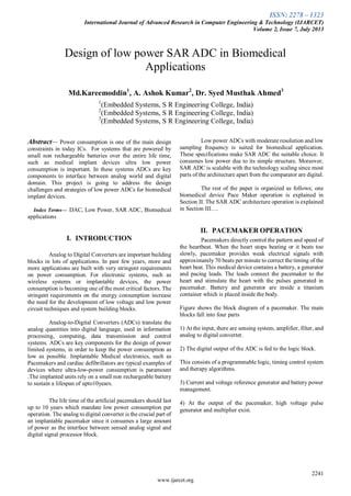
II. PACEMAKER OPERATION
Pacemakers directly control the pattern and speed of
the heartbeat. When the heart stops beating or it beats too
slowly, pacemaker provides weak electrical signals with
approximately 70 beats per minute to correct the timing of the
heart beat. This medical device contains a battery, a generator
and pacing leads. The leads connect the pacemaker to the
heart and stimulate the heart with the pulses generated in
pacemaker. Battery and generator are inside a titanium
container which is placed inside the body.
Figure shows the block diagram of a pacemaker. The main
blocks fall into four parts
1) At the input, there are sensing system, amplifier, filter, and
analog to digital converter.
2) The digital output of the ADC is fed to the logic block.
This consists of a programmable logic, timing control system
and therapy algorithms.
3) Current and voltage reference generator and battery power
management.
4) At the output of the pacemaker, high voltage pulse
generator and multiplier exist.
Design of low power SAR ADC in Biomedical
Applications
Md.Kareemoddin1
, A. Ashok Kumar2
, Dr. Syed Musthak Ahmed3
1
(Embedded Systems, S R Engineering College, India)
2
(Embedded Systems, S R Engineering College, India)
3
(Embedded Systems, S R Engineering College, India)
2. ISSN: 2278 – 1323
International Journal of Advanced Research in Computer Engineering & Technology (IJARCET)
Volume 2, Issue 7, July 2013
www.ijarcet.org
2242
Fig 1: Functional Blocks of Peace Maker
III. SUCCESSIVE APPROXIMATION ADC
This section describes different components of SAR ADC
architecture. The main components of SAR ADC are a
Sample and Hold, a Digital to Analog Converter (DAC), a
Comparator and a SAR Logic.
Fig 2: Sample & Hold
A. Sample & Hold
The Sample & Hold uses a capacitor and an analog switch to
connect or isolate the capacitor from the input. An
operational amplifier connected as follower avoids the effects
of the load. The amplifier can be powered down in order to
reduce the power consumption when the circuit is in the
standby mode.
The most basic form of the sample and hold circuit combines
a switch and a capacitor, the operation of the circuit as
follows. In sampling mode the switch is “on”, creating the
signal path that allows the capacitor to track an input voltage.
When the switch is “off” an open circuit is created that
isolates the capacitor from the input, hence changing the
circuit from sampling mode into holding mode.
B) Digital to Analog Converter
The Digital to Analog Converter has a resolution of 8 bits.
The converter has been divided into two 4 bits D/A
converters to reduce the total area. Each block can be
powered down independently to reduce the power
consumption.
In this architecture we are using R-2R ladder network DAC.
The advantage of the R-2R ladder method is only two values
of resistors are used greatly simplifying the task of matching
or trimming and temperature tracking. Since the output of the
R-2R DAC is the product of the reference voltage & digital
input word, the R-2R ladder DAC is often called as MDAC.
C) Comparator
The comparator is an essential part in the SAR ADC to
perform the binary search algorithm. Comparator in the SAR
ADC takes more power consumption than the other blocks. A
comparator generates a logic output high or low based on the
comparison of the analog input with a reference voltage.
In an ideal comparator, with infinite gain, for input
voltages higher than the reference voltage, the comparator
outputs logical one and for the input voltages lower than the
reference voltage it produces zero at the output.
D) SAR LOGIC
Successive Approximation Register (SAR) control
logic determines each bit successively. The SA register
contains N bit for an N-bit ADC. There are 3 possibilities for
each bit, it can be set to ‘1’, reset to ‘0’ or keeps its value. In
the first step, MSB is set to ‘1’ and other bits are reset to ‘0’,
the digital word is converted to the analog value through
DAC. The analog signal at the output of the DAC is inserted
to the input of the comparator and is compared to the
sampled input.
Based on the comparator result, the SAR controller
defines the MSB value. If the input is higher than the output
of the DAC, the MSB remains at ‘1’, otherwise it is reset to
‘0’. The rest of bits are determined in the same manner. In the
last cycle, the converted digital word is stored. Therefore, an
N-bit SAR ADC takes N+1 clock cycles to perform a
conversion.
Successive approximation register ADC implements the
binary search algorithm using SAR control logic.
In general, there are mainly two fundamentally different
approaches to designing the SAR logic. The first one which is
proposed by Anderson consists of a ring counter and a shift
register. At least 2N flip flops are employed in this kind of
SAR. The other, which is proposed by Rossi, contains N flip
flops and some combinational logic.
3. ISSN: 2278 – 1323
International Journal of Advanced Research in Computer Engineering & Technology (IJARCET)
Volume 2, Issue 7, July 2013
2243
www.ijarcet.org
IV. EXPERIMENTAL RESULTS
A) Sample & Hold
In below figure voltage follower is placed after the
capacitor in order to avoid the loading effect on the capacitor.
The S/H operation is conceptually illustrated by the circuit
shown. The opening and closing of the switch or sampler is
controlled by a sample command (i.e., clock).
Fig 3: Design Of Sample & Hold
When the switch is closed (clk=‘1’), the capacitor C charges
that is samples and tracks the input signal. When the switch
opened (clk=’0’), the output is held at the voltage that the
capacitor is charged to at Vo, until the next sampling pulse
arrives (clk=’1’). The time interval during which the sampler
is closed is called the sampling duration period P.
Fig 4: Sample & Hold Waveforms
B) Comparator
A comparator generates a logic output high or low based on
the comparison of the analog input with a reference voltage.
The comparator in the SAR ADC takes more power
consumption than other blocks. In SAR ADC we must design
comparator such that it consumes very less power.
Fig 5: Design of Comparator
In the below Figure ‘In-‘given to the -ve terminal and the In+
given to the +ve terminal of comparator, when In+ > In- the
output is Out (5 volts) and 0 volts when In+ < In-.
Fig 6: Waveforms of Comparator
C) SAR Logic
This control logic encompasses a ring counter and a code
register. The ring counter is in fact a shift register. In each
clock cycle, one of the outputs in the ring counter sets a Flip
Flop in the code register. The output of this Flip Flop which
is set by the ring counter is used as the clock signal for the
4. ISSN: 2278 – 1323
International Journal of Advanced Research in Computer Engineering & Technology (IJARCET)
Volume 2, Issue 7, July 2013
www.ijarcet.org
2244
previous Flip Flop. At rising edge of the clock, this Flip Flop
loads the result from the comparator.
Fig 7: SAR logic
The Flip Flops which are employed in this structure are
set-reset D-FFs. For low power purpose, transmission gate
based Flip Flops are used . Minimum size transistors with
double length are chosen for improving the power
performance.
Fig 8: Waveforms of SAR logic
D) SAR ADC
Fig 9: Waveforms of SAR ADC
Fig 10: Waveforms of SAR ADC
The power consumption of this ADC mainly
depends upon the performance of the comparator. The power
consumption of the other components such as SAR LOGIC,
DAC and D- Flip Flops are negligible.
As the D-Flip Flops and SAR logic are the digital
components they consume less power compared to analog
ones. Also R-2R DAC consumes less power compared to
comparator during the process
V. CONCLUSION
A successive approximation ADC is suitable for operation
at ultra low supply voltage is realized in a 0.13um CMOS
technology using standard threshold CMOS devices and
avoiding the bootstrapping techniques. This SAR ADC is
well suited for biomedical applications such as Pacemaker,
MRI and EEGs.
REFERENCES
[1] Rudy van de Plassche, “CMOS Integrated
Analog-to-Digital and Digital-to-Analog Converters” 2nd
Edition, Springer International Edition.
[2] John F. Wakerly, “Digital Design Principles and
Practices”, 3rd
Edition, Pearson Education.
[3] Randall L.Geiger, Phillip E.Allen and Noel R.Strader,
“VLSI Design Techniques For Analog And Digital
Circuits”, McGraw-Hill Inc,1990.
[4] Hui Zhang, Yajie Qin, Zhiliang Hong. A 1.8-V 770-nW
Biopotential Acquisition System for Portable
Applications. IEEE Proc. Biomedical Circuits and
Systems Conference, 2009: 93
[5] Naveen Verma, A.P. Chandrakasan. An Ultra Low
Energy 12- bit Rate-Resolution Scalable SAR ADC for
Wireless Sensor Nodes. IEEE J. Solid-State Circuits,
2007, 42(6): 1196.
5. ISSN: 2278 – 1323
International Journal of Advanced Research in Computer Engineering & Technology (IJARCET)
Volume 2, Issue 7, July 2013
2245
www.ijarcet.org
[6] Douglas A.Pucknell & Kamran Eshraghian, “Basic
VLSI Design”, 3rd
Edition, Prentice Hall of India
Pvt.Ltd.
[7] R.Jacob Baker, Harry W. Li, David E. Boyce, “CMOS
Circuit Design, Layout and Simulation”.
Authors Biography
Md. Kareemoddin was born in Karimnagar district, A.P,
India. He received B-Tech in Electronics and
Communication Engineering from Kamala Institute of
Technology and Sciences, Karimnagar (dist), A.P, India.
Perusing M. Tech in Embedded Systems at SR Engineering
College, Warangal, A.P, India.
A.ASHOK KUMAR received M-Tech from SR Engineering
College, Warangal, A.P, India. He is working as Assistant
Professor for dept of Electronics and Communication
Engineering, SR Engineering College, Warangal, A.P, India.
He has 6 years of teaching experience in reputed engineering
colleges. His research interests include VLSI and Embedded
Systems.
Dr.SyedMusthaqAhmed(Prof) completed B.E(Electronics)
and M.E(Electronics) from Bangalore university(Karnataka)
and PhD from Vinayaka Mission’s University (Tamil
Nadu).He has 28 years of teaching experience in reputed
engineering colleges and he is presently working as Prof
&HOD(ECE), SR Engineering college, warangal, A.P. He is
Doctoral committee member as well as Indian examiner in
reputed universities. He is a member of various professional
societies viz SMIEE, MISSS FITEE, MISTE, MIAENG,
MIATM. He has various publications in National &
International Journal/Conferences.