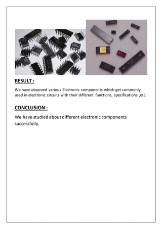
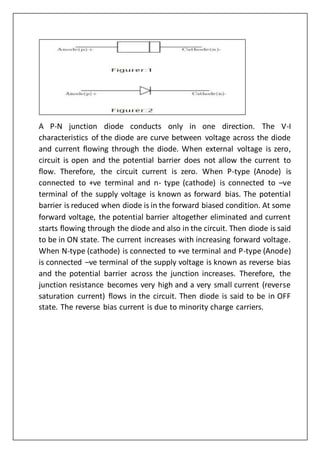
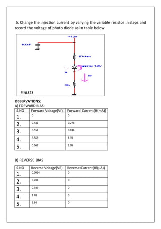
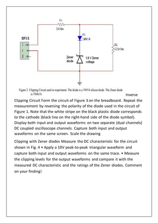
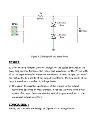
This document outlines various electronic components studied in a practical experiment at the G H Raisoni Institute of Engineering & Technology, focusing on their specifications, theories, and applications. It details the characteristics and functions of resistors, capacitors, inductors, diodes, LEDs, transistors, transformers, fuses, and integrated circuits, along with experimental procedures to observe their behavior. The document concludes that the experiments successfully enhanced understanding of these components and their roles in electronic circuits.


![Experiment No: 6
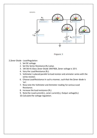
TITLE : Obtain ripple factor of Half wave /Full Wave Rectifier circuit with &
Without Filter.
AIM: 1) To study the operation of half wave and full wave Rectifier
without filter .
To find it’s:
1. Ripple factor
APPARATUS:
Name Range Quantity
CRO (0-20) MHz 1
CRO probes 2
Digital ammeter,
voltmeter
(0-200A/200Ma, [0-20v] 1
Transformer 220v/9v,50Hz 1
Connecting wires
Specification:-
Silicon diode 1N4007:
Max’s forward current=1A
Max’s forward current=0.5 A
Max’s forward voltage=0.8 v
Max reverse voltage=1000V
Max power dissipation=30mW
Temperature=-65 to 200C
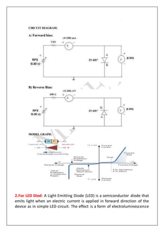
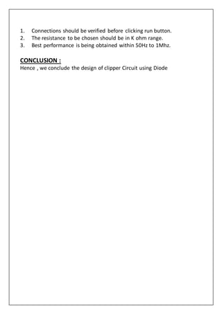
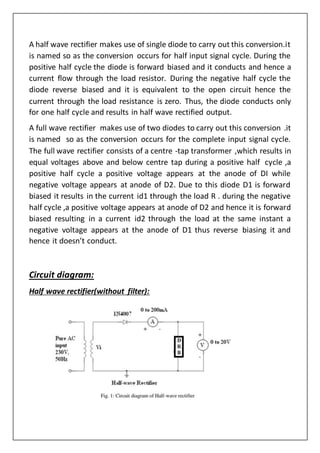
THEORY :A rectifier is circuit that converts a pure AC signal into pulsating
DC signal or a signal that is a combination of AC and DC components](https://image.slidesharecdn.com/iddcpracticles12345678910d24sakshigawade-210618075011/85/Iddc-practicles-1-2-3-4-5-6-7-8-9-10-by-sakshi-gawade-30-320.jpg)

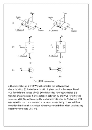
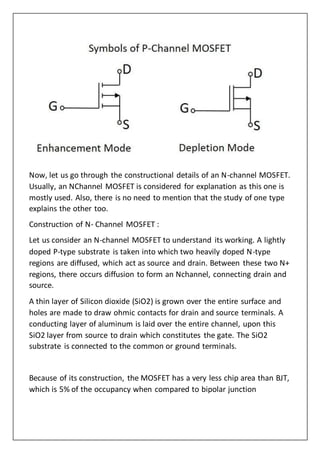
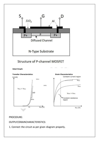
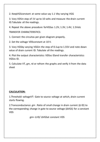
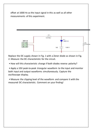
![As shown in Fig.1, it can be fabricated with either an N-channel or P-
channel though N channel is generally preferred. For fabricating an N-
channel JFET, first a narrow bar of N type semiconductor material is taken
and then two P-type junctions are diffused on opposite sides of its middle
part [Fig.1 (a)]. These junctions form two P-N diodes or gates and the area
between these gates is called channel. The two P-regions are internally
connected and a single Electronics Laboratory lead is brought out which is
called gate terminal. Ohmic contacts (direct electrical connections) are
made at the two ends of the bar-one lead is called source terminal S and
the other drain terminal D. When potential difference is established
between drain and source, current flows along the length of the ‘bar’
through the channel located between the two P regions. The current
consists of only majority carriers which, in the present case, are electrons.
P-channel JFET is similar in construction except that it uses P-type bar and
two Ntype junctions. The majority carriers are holes which flow through
the channel located between the two N-regions or gates. Following FET
notation is worth remembering:
1. Source. It is the terminal through which majority carriers enter the bar.
Since carriers come from it, it is called the source.](https://image.slidesharecdn.com/iddcpracticles12345678910d24sakshigawade-210618075011/85/Iddc-practicles-1-2-3-4-5-6-7-8-9-10-by-sakshi-gawade-44-320.jpg)