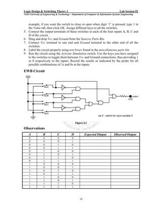
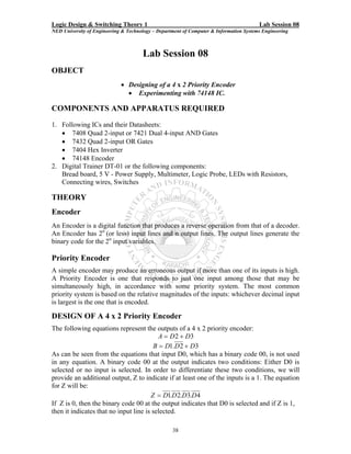
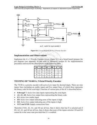
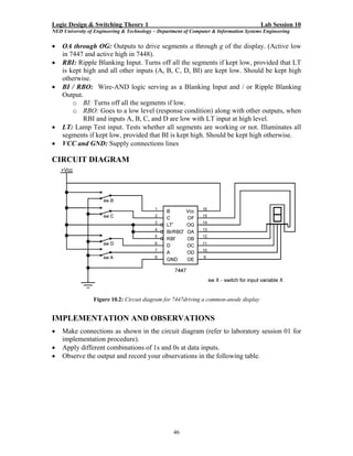
Downloaded 428 times


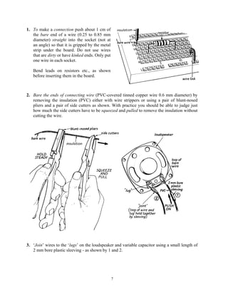


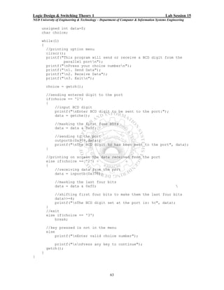


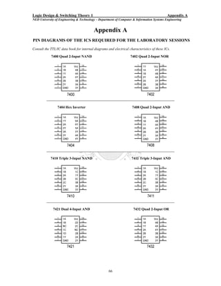

Here are the key steps to test the logic gates: 1. Connect the power supply (5V) and ground to the IC. 2. Apply different combinations of logic inputs (0V, 5V) to the input pins of each gate. 3. Observe the output pin of each gate using an LED or logic probe for the expected output based on the gate's truth table. 4. Record the observed outputs and compare them to the expected outputs based on the gate's function. 5. Test all the gates in the given ICs (AND, OR, NOT, NAND, NOR) following the same procedure. 6. Note any discrepancies between observed and expected outputs.