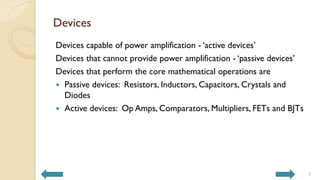
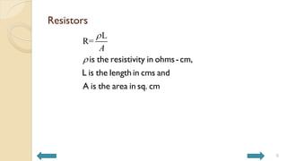
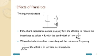
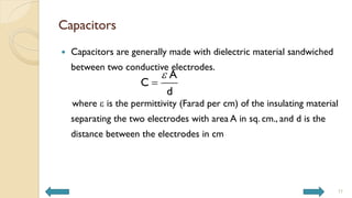
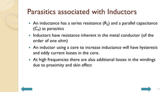
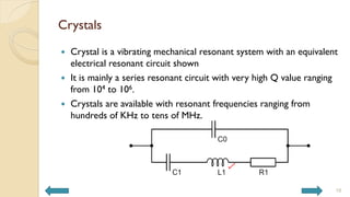
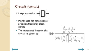
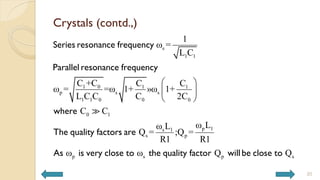
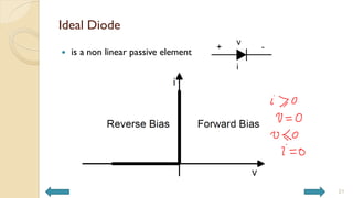
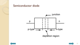
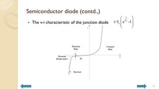
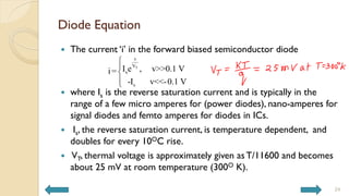
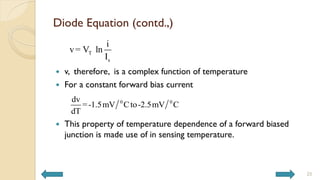
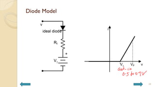
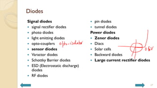
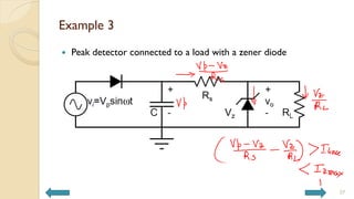
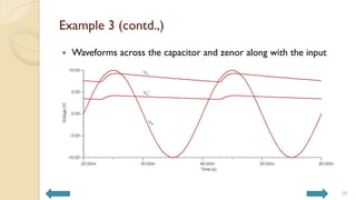
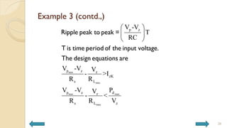
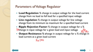
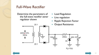
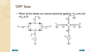
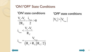
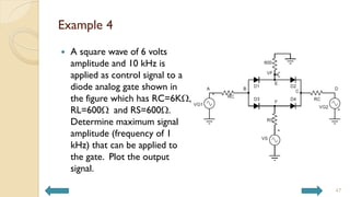
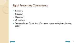
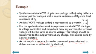
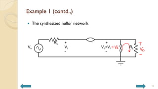
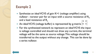
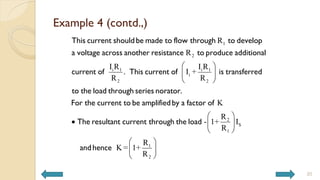
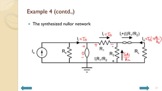
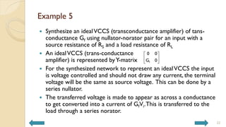
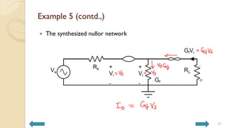
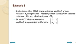
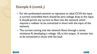
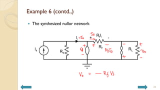
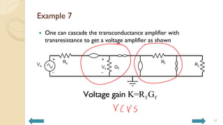
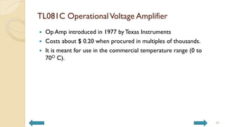
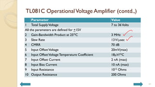
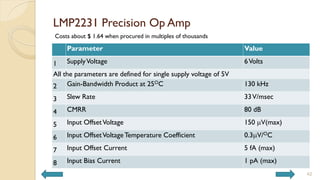
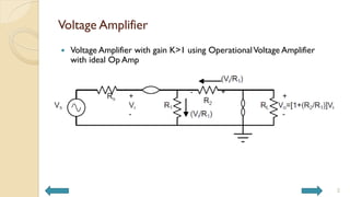
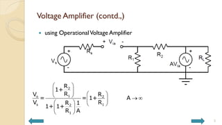
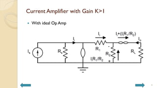
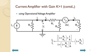
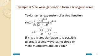
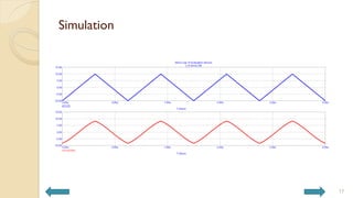
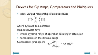
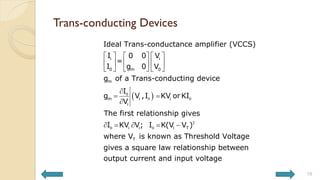
Analog Circuits and Systems
Prof. K Radhakrishna Rao
Lecture 7
1
Passive Electronic Devices for
Analog Signal Processing
2
Analog signal processing functions
 Attenuation
 Amplification
 Filtering
 Amplitude modulation and
demodulation
 Frequency modulation and
demodulation
 Mixing (modulation and
demodulation)
 Digital-to-Analog Converter
 Analog-to-Digital Converter
 Automatic gain control
 Power amplification
 Power supply management
 Signal generation (clock)
3
Mathematical Operations
All analog signal processing functions can be performed through
 Multiplication of a variable by a constant
 Multiplication of two variables
 Comparison
4
Devices
Devices capable of power amplification - ‘active devices’
Devices that cannot provide power amplification - ‘passive devices’
Devices that perform the core mathematical operations are
 Passive devices: Resistors, Inductors, Capacitors, Crystals and
Diodes
 Active devices: Op Amps, Comparators, Multipliers, FETs and BJTs
5
Resistors
L
R=
A

 is the resistivity in ohms-cm,
L is the length in cms and
A is the area in sq. cm
6
Resistors
are commercially made
 from materials including carbon, wires, metal film and
semiconductors
 available from a fraction of an ohm to several mega ohms
 available with varying tolerances (0.1, 0.5, 1, 5, 10 and 20%)
 for different power capacities
 available in different formats (packages) including axial lead devices
and surface mount devices
7
Resistor
can have
 parallel parasitic capacitance
 series inductance
 thermal noise voltage sources
Parasitics become important in high frequency and high precision
analog signal processing circuits
8
Effects of Parasitics
The equivalent circuit
 If the shunt capacitance comes into play first the effect is to reduce the
impedance to values < R with the band width of
 When the inductive effect comes beyond the resonance frequency
of the effect is to increase net impedance
9
P
1
=
RC

P P
1
L C
Effects of Parasitics
 Wire-wound resistors become unusable above 50 kHz
 Carbon type resistors are usable up to around 1 MHz
 Foil resistors can cope up with frequencies up to 100 MHz
10
Capacitors
 Capacitors are generally made with dielectric material sandwiched
between two conductive electrodes.
where e is the permittivity (Farad per cm) of the insulating material
separating the two electrodes with area A in sq. cm., and d is the
distance between the electrodes in cm
e

A
C
d
11
Capacitors (contd.)
 The popular dielectric materials used are ceramic, tantalum,
polyester (Mylar), polystyrene, polypropylene, polycarbonate,
metalized paper, Teflon, air etc.
 Electrode materials mainly include aluminium and silver
 Energy is stored in the capacitors as charge in electrostatic form
given by 0.5CV2 Joules
 Polarized Capacitors have pre-specified polarity and offer large
capacitance values
12
Capacitors (contd.)
are made commercially available
 from a few pico-farads to several hundreds of micro-farads
 with different voltage rating values
 in different formats including axial lead devices and surface mount
devices
Capacitors have leakage resistance, equivalent series resistance (ESR)
ranging from a 0.01 to several Ohms, and lead inductance.
The effects of these parasitics become important in some of the
analog signal processing circuits
13
Effects of Parasitics
Equivalent circuit is a series RLC circuit
 As frequency increases the net impedance decreases
 When the inductive effect comes beyond the resonance frequency
of the effect is to increase net impedance
 Electrolytic capacitors behave as inductors beyond a few MHz,
which is why small ceramic capacitors are put in parallel with them
 Aluminium and tantalum electrolytic capacitors with non solid
electrolyte have high ESR values, up to several ohms
14
P
1
L C
Inductors
 Inductors are coils on a substrate or coils wound around magnetic cores
 Unlike resistors and capacitors inductors are not so easily made available
commercially
 They are generally made to order and hence are costly
 Because of their inconvenient sizes, particularly at low frequencies,
inductors are generally avoided in present day electronics.
m is permeability in Henries per cm, N is the number of turns, A is the
cross section area of the coil in cm2 and l is the length of the coil in cm
2
N
L =
l
A
m
15
Inductors (contd.,)
Inductor also has an important parameter associated with it:
 Quality Factor
where  is the operating frequency in radians/sec.
 Inductors store energy given by 0.5LI2 Joules in electromagnetic
form
S
ωL
Q =
R
16
Parasitics associated with Inductors
 An inductance has a series resistance (RS) and a parallel capacitance
(CP) as parasitics
 Inductors have resistance inherent in the metal conductor (of the
order of one ohm)
 An inductor using a core to increase inductance will have hysteresis
and eddy current losses in the core.
 At high frequencies there are also additional losses in the windings
due to proximity and skin effect
17
Crystals
 Crystal is a vibrating mechanical resonant system with an equivalent
electrical resonant circuit shown
 It is mainly a series resonant circuit with very high Q value ranging
from 104 to 106.
 Crystals are available with resonant frequencies ranging from
hundreds of KHz to tens of MHz.
18
Crystals (contd.,)
It is represented as
 Mainly used for generation of
precision frequency clock
signals
 The impedance function of a
crystal is given by  
 
2
2
s s
s
2 2
p
0 2
s p p
p
s s 1
+ +1
ω Q
ω
Z s =
ω s s 1
s×C + +1
ω ω Q
ω
 
 
 
 
 
 
 
 
 
   
19
Crystals (contd.,)
s
1 1
1 0 1 1
p s s
1 1 0 0 0
0 1
p 1
s 1
s p
p s
1
ω =
L C
C +C C C
ω = =ω 1+ »ω 1+
L C C C 2C
C C
ω L
ω L
Q = ;Q =
R1 R1
ω ω
 
 
 
Series resonance frequency
Parallel resonance frequency
where
The quality factors are
As is very close to the quality facto p s
Q Q
r will be close to
20
Ideal Diode
 is a non linear passive element
21
Semiconductor diode
22
Semiconductor diode (contd.,)
 The v-i characteristic of the junction diode T
v
V
s
i=I e -1
 
 
 
 
23
Diode Equation
 The current ‘i’ in the forward biased semiconductor diode
 where Is is the reverse saturation current and is typically in the
range of a few micro amperes for (power diodes), nano-amperes for
signal diodes and femto amperes for diodes in ICs.
 Is, the reverse saturation current, is temperature dependent, and
doubles for every 10OC rise.
 VT, thermal voltage is approximately given as T/11600 and becomes
about 25 mV at room temperature (300O K).
T
v
V
s
s
I e , v>>0.1 V
i=
-I v<<-0.1 V





24
Diode Equation (contd.,)
 v, therefore, is a complex function of temperature
 For a constant forward bias current
 This property of temperature dependence of a forward biased
junction is made use of in sensing temperature.
T
s
i
v= V ln
I
0 0
dv
=-1.5mV Cto-2.5mV C
dT
25
Diode Model
26
Diodes
Signal diodes
 signal rectifier diodes
 photo diodes
 light emitting diodes
 opto-couplers
 sensor diodes
 Varactor diodes
 Schottky Barrier diodes
 ESD (Electrostatic discharge)
diodes
 RF diodes
 pin diodes
 tunnel diodes
Power diodes
 Zener diodes
 Diacs
 Solar cells
 Backward diodes
 Large current rectifier diodes
27
Diodes (contd.,)
 Signal rectifier diodes are less and less used in present day
electronic circuits.
 The power diodes require special arrangement in the form of heat
sinks to dissipate the heat generated
28
Zener Diodes
 Zenor Diodes are manufactured for operating specifically in the
breakdown region
29
Zener Diodes (contd.,)
 
 
 
zK
D
0
c
I
P
T % C
knee current and
maximum power dissipation
temperature coefficient
30
Zener diodes
 are available in the range of a few volts to a few tens of volts
 zener resistance Rz in the working range of currents is in the range
of a few ohms to tens of ohms
 knee current IzK is typically a few hundred micro amperes
 Temperature coefficient is negative for voltages less than 3V, zero
for 3V, and positive for voltages greater than 3V
Toshiba CMZB12 is a 12V zener of one watt power dissipation and
has a maximum leakage current of 10 mA (Max), RZ=30 Ohms
(Max) and a temperature coefficient of 13 mV/OC (Max)
31
Sensor Diodes
 Two matched diodes in one
package can be used as a
temperature sensor
1 2
1 2
ln ; ln
11,600
S S
kT I kT I
V V
q I q I
q
k
 

where k is Boltzman's constant,
q is electronic charge, and
32
Sensor Diodes (contd.,)
S
1 2
As the diodes are matched(same I )
the differential voltage
Temperature sensor whose
coefficient is
where I andI are determined
by the designer
1
1 2
2
1
2
kT I
V -V = ln
q I
k I
ln ;
q I
 The coefficient is less sensitive
to the variations in diode
currents because of the
logarithmic relationship
 S5813A from Seiko
Instrument is one such sensor
with a sensitivity of
11.04 mV/OC and output
voltage of 1.94 volts at
+30OC.
33
Example 1
 Half wave rectifier
34
Example 1 (contd.,)
 Input voltage is a
sinusoidal wave of 2V
amplitude and 50 Hz
35
Example 2
 Peak detector
36
Example 3
 Peak detector connected to a load with a zener diode
37
Example 3 (contd.,)
 Waveforms across the capacitor and zenor along with the input
38
Example 3 (contd.,)
min
min
max max
max
p z
p z z
zK
s L
p z d
z
s L z
V -V
T
RC
V -V V
- >I
R R
V -V P
V
- <
R R V
 
 
 
Ripple peak to peak =
T is time period of the input voltage.
The design equations are
39
Parameters ofVoltage Regulator
 Load Regulation: % change in output voltage for the load current
change from no load to full load for a specified input voltage
 Line regulation: % change in output voltage for line voltage
change from its minimum to maximum for a specified load current
 Ripple Rejection Factor: % change in output voltage for a %
change in input voltage for a given load and input voltage
 Output Resistance: % change in output voltage for a % change in
load current at a given load current
40
Full-Wave Rectifier
Determine the parameters of
the full-wave rectifier zener
regulator shown
 Load Regulation
 Line regulation
 Ripple Rejection Factor
 Output Resistance
41
Analog Gate (Diode Multiplexer)
 Analog gate enables an analog
signal source to be connected
or disconnected to a load
 Diode bridge is switched ‘on’
by dc current by applying
+Vc at A and -Vc at D
 Diode bridge is switched ‘off’
by dc voltage by applying -Vn
at A and +Vn at D
42
Analog Gate (Diode Multiplexer) (contd.,)
43
‘ON’ State
 When all the diodes (D1, D2, D3 and D4 ) are conducting
44
‘OFF’ State
 When all the diodes are reverse biased by applying –VN at A and
+VN at D
45
‘ON’/’OFF’ State Conditions
 
max
max
max
max
s
c
C
c
s
C
s
s
s L C
i
V -V
- >0
2R 2
V -V
i <
R
V
i =
R +R R 2


'ON' state conditions
max
n s
V > V
'OFF' state conditions
46
Example 4
 A square wave of 6 volts
amplitude and 10 kHz is
applied as control signal to a
diode analog gate shown in
the figure which has RC=6KW,
RL=600W and RS=600W.
Determine maximum signal
amplitude (frequency of 1
kHz) that can be applied to
the gate. Plot the output
signal.
47
Example 4 (contd.,)
s
s
s
s
s
V
6-0.6
>
0.6×3
6 0.6+
3.6
V
0.93> ; V <0.93×1.1 =1.023V
0.6+0.5
V <6V
V
When the gate is ON
When the gate is OFF
Therefore shouldbe less than1V
48
Example 4 (contd.,)
 Plot of the output voltage for
T
Time (s)
0.00 250.00u 500.00u 750.00u 1.00m
Voltage
(V)
-800.00m
-600.00m
-400.00m
-200.00m
0.00
200.00m
400.00m
600.00m
800.00m
s
V =0.8sin 2000 t

49
Conclusion
50
Analog Circuits and Systems
Prof. K Radhakrishna Rao
Lecture 8
Active Devices for Analog Signal Processing Systems
1
Signal Processing Components
 Resistor,
 Inductor
 Capacitor
 Crystal and
 Semiconductor Diode (rectifier, zener, sensor, multiplexer {analog
gate})
2
Active Devices for Analog Signal
Processing Systems
3
Active Devices
 Op Amps
 Comparators
 Multipliers
 BJT
 FET
4
Op Amps
 They are called so as they are used to perform several
mathematical operations including addition, subtraction,
integration and differentiation
5
Ideal Op Amp Input-Output Characteristic
 For any finite output, the input voltage and input current are zero
6
Ideal Op Amp
 Ideal Op Amp is an ideal amplifier whose transfer
parameter, pf, goes to infinity
 To model an Ideal Op Amp we require
 An input network element that does not draw any current and has
zero voltage across it. (Vi=0, Ii=0) It is known as Nullator
 An output network element that is source that can provide any
current demanded by the load and can develop any voltage across
the load. It is known as Norator
 A nullator along with its companion norator is called ‘nullor’
 Every nullator has a companion norator
7
0 0
0
f
p
 
 
 
Nullator-Norator representation of Ideal Op Amp
 Ideal Op Amp is represented by a nullator - norator pair
8
Ideal DIDO Op Amps
 An ideal Differential Input Differential Output Amplifier (DIDO)
with infinite differential gain
9
Ideal DISO Op Amps
 Ideal Differential Input Single Ended Output Amplifier (DISO)
with infinite gain.
10
Ideal SISO Op Amps
 Ideal Single Input Single Ended Output Amplifier (SISO) with
infinite gain.
11
Example 1
 Synthesize an idealVCVS of gain one (voltage buffer) using nullator -
norator pair for an input with a source resistance of RS and a load
resistance of RL
 An idealVCVS (voltage buffer) is represented by g-matrix
 For the synthesized network to represent an idealVCVS the input
is voltage controlled and should not draw any current, the terminal
voltage will be the same as source voltage.This voltage should be
transferred to the output without any change. This can be done by
a series nullator.
 At the output a norator has to be connected across the load to
deliver current as demanded by the load
12
0 0
1 0
 
 
 
Example 1 (contd.,)
 The synthesized nullor network
13
Example 2
 Synthesize an idealVCVS of gain K>1 (voltage amplifier) using
nullator - norator pair for an input with a source resistance of RS
and a load resistance of RL
 An idealVCVS (voltage buffer) is represented by g-matrix
 For the synthesized network to represent an idealVCVS the input
is voltage controlled and should not draw any current, the terminal
voltage will be the same as source voltage.This voltage should be
transferred to the output without any change. This can be done by
a series nullator.
14
0 0
K 0
 
 
 
Example 2 (contd.,)
For the voltage to be amplified by a factor of K
 Series nullator facilitate the transfer ofVS
 Connect a resistance R1 across the transferred voltageVS to
generate a current (VS/R1)
 Introduce a resistor R2 in series with R1 to boost up the voltage by
(VS/R1) R2
 The resultant voltage across R1 and R2 is and hence
At the output a norator has to be connected across the load to
deliver current as demanded by the load
15
2
S
1
R
(1+ )V
R
2
1
R
K=(1+ )
R
Example 2 (contd.,)
 The synthesized nullor network
16
Example 3
 Synthesize an ideal CCCS of gain one (current buffer) using nullator
- norator pair for an input with a source resistance of RS and a load
resistance of RL
 An ideal CCCS (voltage buffer) is represented by h-matrix
 For the synthesized network to represent an ideal CCCS the input
is current controlled there should be zero voltage drop at the input.
It should permit any current to flow into the network which
requires a nullator to be connected in shunt with the input of the
network.
 At the output a norator has to be connected in series with the load
to deliver a current same as input current to the load and to
support the developed voltage across the load.
17
0 0
-1 0
 
 
 
Example 3 (contd.,)
 The synthesized nullor network
18
Example 4
 Synthesize an ideal CCCS of gain K>1 (current amplifier) using
nullator - norator pair for an input with a source resistance of RS
and a load resistance of RL
 An ideal CCCS (current amplifier) is represented by h-matrix
 For the synthesized network to represent an ideal CCCS the input
is current controlled there should be zero voltage drop at the input.
It should permit any current to flow into the network which
requires a nullator to be connected in shunt with the input of the
network.
19
0 0
-K 0
 
 
 
Example 4 (contd.,)
20
1
2
i 1 i 1
i
2 2
R
R
I R I R
. I +
R R
 
 
 
This current shouldbe made to flow through to develop
a voltage across another resistance to produce additional
current of This current of is transferred
to the load th
2
S
1
1
2
K
R
- 1+ I
R
R
K = 1+
R
 
  
 
 
 
 
rough series norator.
For the current to be amplifiedby a factor of
The resultant current through the load
andhence
Example 4 (contd.,)
 The synthesized nullor network
21
Example 5
 Synthesize an idealVCCS (transconductance amplifier) of tans-
conductance Gf using nullator-norator pair for an input with a
source resistance of RS and a load resistance of RL
 An idealVCCS (trans-conductance
amplifier) is represented byY-matrix
 For the synthesized network to represent an idealVCCS the input
is voltage controlled and should not draw any current, the terminal
voltage will be the same as source voltage. This can be done by a
series nullator.
 The transferred voltage is made to appear as across a conductance
to get converted into a current of GfVi.This is transferred to the
load through a series norator.
22
f
0 0
G 0
 
 
 
Example 5 (contd.,)
 The synthesized nullor network
23
Example 6
 Synthesize an ideal CCVS (trans-resistance amplifier) of tans-
resistance Rf using nullator - norator pair for an input with a source
resistance of RS and a load resistance of RL
 An ideal CCVS (trans-resistance
amplifier) is represented by Z-matrix
24
f
0 0
-R 0
 
 
 
Example 6 (contd.,)
 For the synthesized network to represent an ideal CCVS the input
is current controlled there should be zero voltage drop at the input.
It should permit any current to flow into the network which
requires a nullator to be connected in shunt with the input of the
network.
 The current coming into the network flows through a series
resistance Rf developing a voltage -IiRf at the output. A norator has
to be connected in shunt with the load.
25
Example 6 (contd.,)
 The synthesized nullor network
26
Example 7
 One can cascade the transconductance amplifier with
transresistance to get a voltage amplifier as shown
27
f f
K=R G
Voltage gain
Example 8
 One can cascade the transresistance amplifier with
transconductance to get a current amplifier as shown
28
f f
K=R G
Current gain
Types of Commercial Op Amps
 Operational Trans-conductance Amplifier
 Operational Trans-resistance Amplifier
 OperationalVoltage Amplifier
 Operational Current Amplifier
29
CMRR
30
   
   
   
   
0 offset 1 1 2 2 1 2
1 2 1 2 1 2 1 2
0 1 2
V =V +K V +K V +nonlinear functionsof V andV
V V V V
V = K + + K -
2 2 2 2
V V V V
CMRR (contd.,)
31
 


 
 
 


1 2
C
d 1 2
1 2
0 1 2 C d
C
d
1 2 C d
1 2
CommonMode Voltage V =
2
Differential Mode Voltage V =
K -K
V = K +K V + V
2
A
A
In a symmetric structure K =-K =K A =0 and A =K
Ideal CMRR =
When K K the circuit is asymmetric and
d
C
d
V V
V V
A
A
A
A
is high but finite
C
Op Amps
 Op Amps operate with single or dual DC power supply voltages
 Output cannot go beyond power supply voltages
 Finite, but large, dc gain, dependent on the frequency and signal level
(non-linearity)
 Off-set voltages and currents
 Finite input impedance, and finite output impedance
 Finite Common Mode Rejection Ratio (CMRR)
 All the parameters of an Op Amp also depend on the temperature
32
OperationalVoltage Amplifier Static Characteristic
33
0
S1 S2
0
S1 S2
is maximum when the
V +V
output voltage is at
2
approaches zero as the
output approaches V or V
i
i
V
V
V
V


 
 
 


Op Amps
 finite gain ranging from 103 to 106 (60 dB to 120dB)
 CMRR is in the range of 70 to 120 dB
 several independent parasitic capacitances associated with internal
nodes, with each capacitance reducing the gain at 20dB/decade
34
Gain transfer function of an Op Amp
35
0
1 2 3
1 2 3
0
1
1 1 1
45
p p p
p p p
A
A
s s s
  
  


     
  
     
     
     
 


where A0 is the dc gain, and are the corner frequencies
Magnitude reduces by 3 dB at the corner frequency
Phase shift becomes at as lo 2 3
0 0 0 0
2 3
0
2 3
0
90 45 180 45
180
270
 
 
 
  


ng as and are much greater than
Phase shift can become at andit can become at
Phase shift becomes at a frequency between and
Phase shift approaches at 3

frequencies greater than
Magnitude and phase responses
36
Op Amps
Mismatches at the inputs cause
 input offset voltage: a few milli volts to a few tens of milli volts,
 input offset current a few nano amperes
If the Op Amp is a voltage amplifier
 input impedance can be from a few MW to a few hundred MW.
 output impedance can be few hundred Ohms
 Output current of majority Op Amps is limited to 20 mA.
37
Slew Rate
 The maximum rate of change of output of an Op Amp is called ‘slew
rate’
 Arises out of limiting current available for charging the capacitor at
the output
 As Op Amps are protected against short circuit at the output, it
limits the output current to 20 to 50 mA.
 Slew rate is expressed asVolts/msec
 It is one to 20Volts/msec
38
GB Product
 Op Amps are characterized by their gain-bandwidth (first corner
frequency) (GB) product
 GB product, a parameter that is used extensively in designing Op
Amp based circuits
 It is typically 1MHz to 20 MHz
39
TL081C OperationalVoltage Amplifier
 Op Amp introduced in 1977 by Texas Instruments
 Costs about $ 0.20 when procured in multiples of thousands.
 It is meant for use in the commercial temperature range (0 to
70O C).
40
TL081C OperationalVoltage Amplifier (contd.,)
Parameter Value
1 Total SupplyVoltage 7 to 36Volts
All the parameters are defined for +15V
2 Gain-Bandwidth Product at 25OC 3 MHz
3 Slew Rate 13V/msec
4 CMRR 70 dB
5 Input OffsetVoltage 20mV(max)
6 Input OffsetVoltageTemperature Coefficient 18mV/OC
7 Input Offset Current 2 nA (max)
8 Input Bias Current 10 nA (max)
9 Input Resistance 1012 Ohms
10 Output Resistance 200 Ohms
41
LMP2231 Precision Op Amp
Parameter Value
1 SupplyVoltage 6Volts
All the parameters are defined for single supply voltage of 5V
2 Gain-Bandwidth Product at 25OC 130 kHz
3 Slew Rate 33V/msec
4 CMRR 80 dB
5 Input OffsetVoltage 150 mV(max)
6 Input OffsetVoltageTemperature Coefficient 0.3mV/OC
7 Input Offset Current 5 fA (max)
8 Input Bias Current 1 pA (max)
42
Costs about $ 1.64 when procured in multiples of thousands
LMH6682 High Speed Op Amp
Parameter Value
1 SupplyVoltage 3-12Volts
All the parameters are defined for single supply voltage of 5V
2 Bandwidth at Gain = 2 140 MHz
3 Slew Rate 520V/msec
4 CMRR 72 dB
5 Input OffsetVoltage +5 mV(max)
6 Input OffsetVoltageTemperature Coefficient +2mV/OC
7 Input Offset Current 300 nA (max)
8 Input Bias Current 20 mA (max)
43
Costs about $ 0.91 when procured in multiples of thousands
OPA860 Transconductance Amplifier
Parameter Value
1 SupplyVoltage +6.5 Volts
All the parameters are defined for single supply voltage of 5V
2 Bandwidth at Gain = 5 80 MHz
3 Transconductance 95 mS
4 Slew Rate 3000V/msec
5 Input OffsetVoltage +38 mV(max)
6 Input OffsetVoltageTemperature Coefficient +120mV/OC
7 Input Bias Current 6.8 mA (max)
44
Costs about $ 5.00 when procured in hundred up quantities
Simulation
45
Conclusion
46
Analog Circuits and Systems
Prof. K Radhakrishna Rao
Lecture 9: Electronic Devices for Analog Circuits
1
Voltage Amplifier
 Voltage Amplifier with gain K>1 using OperationalVoltage Amplifier
with ideal Op Amp
2
Voltage Amplifier (contd.,)
 using OperationalVoltage Amplifier
3
2
1
o 2
s 1
2
1
R
1+
R
V R
= = 1+ A
V R
R 1
1+ 1+
R A
 
 
 
   
 
   
 
 
Current Amplifier with Gain K>1
 With ideal Op Amp
4
Current Amplifier with Gain K>1 (contd.,)
 using OperationalVoltage Amplifier
5
1
2
2 1
1 2
L
2
R 1
1+ +
R A
I R
=- - 1+
I R
R 1
1+ 1+
R A
 
 
 
 
 
 
 
 
   
 
 
Trans-conductance Amplifier
with ideal Op Amp
6
Trans-conductance Amplifier (contd.,)
with OperationalVoltage Amplifier
7
 
f
o i f i
f L
1
G 1
A 1
I V G V
G R
1
A 1
 
 
 
 

 
 
 

 

 
Trans-resistance Amplifier
with ideal Op Amp
8
Trans-resistance Amplifier (contd.,)
with ideal OperationalVoltage Amplifier
9
i f
o i f
I R
V I R
1
1
A

 
 

 
 
Synthesis of a positive resistance
10
Synthesis of a negative resistance
11
i f i
I G V
 
Instrumentation amplifier
Analog Gate (Diode Multiplexer)
 rejects the differential mode control signal
 accepts the common mode sampled signal
Instrumentation Amplifier
 It rejects common mode signal
 Accepts and amplifies only the differential mode signal
Required symmetry is achieved with well matched components which
can be realized readily in integrated circuits
12
Synthesis of Instrumentation Amplifier function
13
Example 1: Instrumentation Amplifier
with ideal operational trans-conductance amplifier
14
1
2
100 0 5 1000
100 0 5 1000
100 100
100 10
ci co
di do
V sin t . sin t
V sin t . sin t
R k,R k
R ,R k
   
   
 
 
Simulation of Instrumentation Amplifier
15
Example 2: Instrumentation Amplifier
 With ideal operational voltage amplifier
16
Simulation of Instrumentation Amplifier
17
Modelling Op Amps
 Create an equivalent circuit of all the active and passive
components internal to the Op Amp (Micro model)
 Create an equivalent circuit that represents input-output behaviour
of the Op Amp (Macro model)
18
Macro Models
Macro model of an Op Amp
 1st level: Nullator-norator (nullor)
 2nd level: Finite high gain current or voltage amplifier
 3rd level: Finite high gain current or voltage amplifier with
attenuation of gain at 20dB per decade (first-order low-pass
filtering)
19
Macro Models Contd.,)
 4th level: Finite high gain current or voltage amplifier with
attenuation of gain at 20dB per decade
 5th level: Finite high gain current or voltage amplifier with
attenuation of gain at 20dB per decade with output voltage swing
limited to supply voltage
 Higher level macro models will take input offset, output current
limitation, slew rate, higher order frequency dependence of gain etc.
20
Macro model
 Earlier examples were synthesized using 1st level macro models
and simulated with 2nd level macro models
 5th level macro model of TL081
21
Comparators
 Comparator is an interface component
 Its input is analog and its output is digital (1/0 or high/low).
 It is a one-bit Analog-to-Digital Converter (ADC)
 The output changes its state when the input voltage crosses a
reference value.
22
Comparator (contd.,)
23
Voltage Comparator Current Comparator
Ideal comparator
 has infinite gain in the active region while transiting from one state to
the other
LM311 comparator (made available by most IC manufacturers & costs
$0. 2 in>1k quantities)
Parameter Value
1 Total SupplyVoltage 3.5 to 30Volts
2 Rise Time 115 ns
3 Common Mode InputVoltage 0.5 to 28V
4 Input OffsetVoltage 7.5 mV (max)
5 Input Offset Current 70 nA (max)
6 Input Bias Current 300 nA (max)
24
OffsetVoltage
25
Input offset voltage (7.5 mV in case of 311)
Commercial comparators
 are designed to have a
forward gain of the order of
100
 Active transition region will be
instead of zero in case of infinite
gain
26
0
u L
V V
A
 

 
 
u L
ioffset
o
V -V
V +
A
 inputreferredoffset
Commercial comparators (contd.,)
27
Example 3: Duty Cycle Generator
 Duty cycle generator
(Pulse width
modulator):
A triangular waveform
with an amplitude of
5V is applied asVi and
Vref = 2.5V? What
happens to the
waveform whenVref is
varied?
28
ref
p
V
1 1
1
T 2 V 4
 

  
 
 
 
Example 3: Duty Cycle Generator (contd.,)
 Duty cycle generator (Pulse width modulator) Simulation
29
Vref = 2.5V
1
T 4


Example 3: Duty Cycle Generator (contd.,)
 Duty cycle generator (Pulse width modulator) Simulation
30
Vref = -2.5V
3
T 4


Conclusion
31
Analog Circuits and Systems
Prof. K Radhakrishna Rao
Lecture 10: Electronic Devices for Analog Circuits
1
Multipliers
Multipliers provide multiplication of two input voltages or currents
Multipliers can perform
 voltage controlled amplification
 filtering
 mixing
 modulating
 demodulating
 phase detection
 signal generation
 frequency synthesis
2
Multipliers
are available commercially as
 voltage controlled amplifiers
 current controlled amplifiers
 digitally controlled amplifiers
3
0
0
0
offset X X Y Y
X Y
offset
X X Y Y
V V K V K V
K V V
V
K V and K V
K
  

Input - Output Characteristic
+non - linear terms
is the DC offset voltage
are feed
through components
is the multiplier constant
andhas the dimension per volts
Multipliers
4
Methods of Multiplication
5
 
2 2
4
X Y X Y X Y
O
R R
O X Y Z
X Y X Y
Z Z
(V V ) (V V ) V V
V
V V
Using squaring devices and adders
V antilog logV logV logV
V V V V
antilog log
V V
Using log and antilog devices and adders
  
  
   
 
 
 
 
MPY634 (precision Multiplier)
 Log-Antilog Multiplier
with -10V <VX,VY < 10V
6
  
 
X1 X2 Y1 Y2
0 Z1 Z2
V -V V -V
V =A - V -V volts
10
 
 
 
MPY634
 The dynamic ranges of inputs and output are compatible with
one another
Parameter Value
1 Bandwidth 6 MHz (min)
2 Slew rate 20V/msec
3 Output OffsetVoltage +100 mV(max)
4 Output Short Circuit Current 30 mA
7
Example 1: Mixer
8
 
1 2
1 1 0 1 2
1 2
2 2 1 2 1 2
10
20
p p
X p
p p
Y p
Double Side Band generator/ Balanced Modulator
V V
V V sin t V sin t sin t
V V
V V sin t cos( )t cos( )t
    
         
Simulation of a Mixer
 For f1 = 10 kHz, f2 = 1 kHz,Vp1 = 2V andVp2 = 1V
9
Simulation of a Mixer (contd.,)
 Output when DC voltage of 1V is added toVY
10
Example 2: Linear Delay Detector
 Vx is a square wave of 10 kHz
 Vy is a delayed (by t) square
wave of 10 kHz
11
Example 2: Linear Delay Detector (contd.,)
12
aV 0
T
-10 10 -
4
2
V of V 10 1
T T
2
 
  
  
 
 
  
 
 
Example 3: Phase Detector
13
x p1
y p2
p1 p2
0
p1 p2
0
av 0
V V sin t
V V sin( t )
V V
V cos cos(2 t )
20
with f=10 kHz, =90
V =V =10 V
V 5 cos cos(2 t )
2 2
5sin2 t
V Ave.of V 0
 
   
     
 
 
 
 
 
   
 
 
 
 
0
0
5 2
3 3
1
5 2
2 3
2 5
av
with = 60
V cos cos( t )
cos( t )
V Ave.of V .
Phase detector is used
measuring reactive power,
active power and power factor

 
 
   
 
 

 
   
 
 
 
Simulation
 with f = 10 kHz,  = 90O,Vp1 =Vp2 = 10V
14
Simulation (contd.,)
 with f = 10 kHz,  = 60O,Vp1 =Vp2 = 10V
15
Example 4: Sine wave generation from a triangular wave
16
 
 
 
   
2n 1
2n 1
n 0
3 5
Taylor series expansion of a sine function
1
sinx x
2n 1 !
x x
x ...
3! 5!
If x is a triangular wave it is possible
to create a sine wave using three or
more multipliers and an adder







   

Simulation
17
Devices for Op Amps, Comparators and Multipliers
 Input–Output relationship of an ideal device
where pf would be a constant
Physical devices have
 limited dynamic range of operation resulting in saturation
 nonlinearities in the dynamic range
Nonlinearity (first order)
18
f
0 0
Y = X
p 0
 
   
 
   
 
 
f
X,Y
Y
p = =KXor KY
X


Trans-conducting Devices
19
 
0
0 0
2
0 0
i i
0 0
m
m
m i i
i
i i i T
T
Ideal Trans-conductance amplifier (VCCS)
I V
0 0
=
I V
g 0
g of a Trans-conducting device
I
g V ,I KV or KI
V
The first relationship gives
I KV V; I K(V V )
where V is known
   
 
   
 
 
   

 

    
as Threshold Voltage
gives a square law relationship between
output current and input voltage
Trans-conducting Devices
 The second relationship gives
where IS is known as Reverse Saturation Current
 Gives an exponential relationship between the output current and
input voltage
20
 
0
0
0
0
ln
1
i
i
i
KV
S
I
K V
I
I KV
I I 

 

 
Semiconductor devices
exhibiting these relationships
 Field Effect Transistors (FETs)
 Bipolar Junction Transistors (BJTs)
FET
 exhibits a square law relationship in the region above threshold
voltage
 exponential relationship in sub-threshold region (Vi <VT)
BJT
 exhibits exponential relationship
21
FET
 Patented by Julius Edgar Lilienfeld in 1926 first and by Oskar Heil in
1934
 Practical semiconducting devices (JFETs) were developed only much
later
 MOSFET (Metal Oxide on Semiconductor Field EffectTransistor)
was invented by Dawon Kahng and Martin Atalla in 1960.
 MOSFETs largely superseded the JFETs and had a more profound
effect on electronic development
22
BJT
 Bipolar point-contact transistor was invented in December 1947 at
the BellTelephone Laboratories by John Bardeen and Walter
Brattain under the direction of William Shockley
 Junction version known as the bipolar junction transistor was
invented by Shockley in 1948
 BJTs enjoyed three decades as the device of choice in the design of
discrete and integrated circuits
23
Present Status
 Discrete MOSFETS are not available commercially because of
problems associated with electro static discharge.
 JFET are available, but their use is not popular in signal processing
 MOSFET technology is dominant in both digital and analog
integrated circuits
 While discrete BJTs were commercially made available for several
decades, their usage at present in signal processing functions has
practically stopped
24
Present Status (contd.,)
 This was mainly due to ready availability of Op Amps and the
requirement of smaller footprints for the electronic systems
 Discrete semiconductor devices at present are mainly available as
power devices including Power MOSFETs and IGBTs
25
Integrated Circuits
 Predominantly use CMOS (Complementary MOSFET) technology,
and BiCMOS (Bipolar and Complementary MOSFET) technology to
a limited extent.
 All digital integrated circuits are manufactured using mostly CMOS
technology
 Some mixed signal circuits are made with BiCMOS technology
 Some Op Amps based on bipolar devices are still produced today
because of their popularity with the users.
26
Why study FETs and BETs
 Design of power electronic circuits
27
Field Effect Transistors
 FET is a four terminal device:‘source’,‘drain’,‘gate’ and ‘substrate’
 Gate-substrate voltage controls the current between the ‘source’
and the ‘drain’.
 Channel can exist between source and drain
 Channel can be created between source and drain by applying
voltage between gate and substrate
 The gate is isolated from the channel by a reverse biased junction
or by an insulator known as gate oxide
28
Field Effect Transistors
JFET
 can be either n-type channel
or p-type channel
 Gate is isolated from channel
by a reverse biased junction
 Channel is always controlled
in depletion mode
MOSFET
 can be either n-type channel
or p-type channel
 Gate is isolated from channel
by insulator
 Channel can be controlled by
either polarity of gate voltage,
that is, control is achieved
through either depletion or
enhancement.
29
Types of FETs
 n-channel JFET
 p-channel JFET
 n-channel depletion mode FET
 p-channel depletion mode FET
 n-channel enhancement mode FET
 p-channel enhancement mode FET
30
Preferred Technology and Devices
 Enhancement mode FETs are the preferred devices as they are
normally off-devices (no channel between source and drain) when
no voltage is applied to gate with respect to the substrate.
 Depletion mode FET technology would have been the natural
choice for analog ICs because the devices are in the active region
with zero DC bias
 As the enhancement mode FET technology is used mainly for digital
ICs, the same technology is also used for analog ICs in view of
higher reliabilities and yields
 Use of a single technology for mixed signal processing ICs
31
FET (n-channel enhancement)
32
 
 
2
2
GS T
DS GS T
DS GS T
DS DS GS
When a voltage V higher than V is applied to the gate;current
through the channel increases in proportion to square of the voltage
K
I V V
For V V V current saturation region and
for V I K V
 
 
     
2
2
DS
T DS
V
V V triode r egion
 
 
 
 
Micro models: Large signal model
33
Micro models: Small signal model
34
 
 
2
DS
m GS T DS
GS
DS GS T
I
where g K V V I K
V
in the region where V V V

   

 
Micro models: Higher order Model
35
   
DS GS T DS DSS OS
DS
ds DSS
DS
V V -V is given by I =I 1+λV
where λ is known as channel length modulation factor
I
g = =λI
V



High frequency equivalent circuit of MOSFET
36
When used in analog integrated circuits
Bipolar Junction Transistor (BJT)
BJT is a three terminal device: emitter, base and collector
Transistor is brought into active region by
 forward biasing the emitter base junction
 reverse biasing the collector base junction
 Types of BJTs: npn and pnp
37
Model of BJT
38
 
BE T
E
V V
E E0
C E
I is the input current. The voltage current relationship
at the base-emitter junction, when it is forward biased
I =I ε
The emitter current is very nearly transported to the collector
I I where
   1 E C B E E B
; I I I ; I I I
    
Model of BJT
39
BE
BE T
T
B C
E
C B B BE T
E0
V
V V
V C EO E
C EO m
BE T T
If I is considered as the input current and I as the output current
I
α
I = I =βI V =V ln
1-α I
Common emitter configuration of the transistor
I I I
I =αI ε g
V V V
  
   

Higher order Micro model
40
300
BE
T
C
CE
V
V CE
C EO
E
E
T
Base width modulation
effects I with respect
to V
V
I =αI ε 1+
V
where V is known as
"Early Voltage"
kT
V = is 26 mV at T K
q
 
 
 
 
C
B
B
C
C C
ce
CE E
δI
β
= where β=
β+1 δI
I is the base current and
I is the collector current
δI I
= =g
δV V

High frequency equivalent of BJT used in ICs
41
Model of Ideal 3-terminal Trans-conducting Device
Represented by
 a nullator at the input port
 a norator at the output port
to make the collector or drain current the same as the emitter or
source current
42
m i
g and finite output; V 0 and Ii 0
    
Synthesis of ideal amplifiers
 VCVS with gain 1
43
Synthesis of ideal amplifiers
 CCCS with gain -1
44
Synthesis of ideal amplifiers
 Trans-conductor Amplifier (VCCS)
45
0 f i
I G V

Synthesis of ideal amplifiers
 Trans-resistance Amplifier (CCVS)
46
0 f i
V R I
 
Conclusion
47

Week 3 - Devices for Analog Signal Processing.pdf

  • 1.
    Analog Circuits andSystems Prof. K Radhakrishna Rao Lecture 7 1
  • 2.
    Passive Electronic Devicesfor Analog Signal Processing 2
  • 3.
    Analog signal processingfunctions  Attenuation  Amplification  Filtering  Amplitude modulation and demodulation  Frequency modulation and demodulation  Mixing (modulation and demodulation)  Digital-to-Analog Converter  Analog-to-Digital Converter  Automatic gain control  Power amplification  Power supply management  Signal generation (clock) 3
  • 4.
    Mathematical Operations All analogsignal processing functions can be performed through  Multiplication of a variable by a constant  Multiplication of two variables  Comparison 4
  • 5.
    Devices Devices capable ofpower amplification - ‘active devices’ Devices that cannot provide power amplification - ‘passive devices’ Devices that perform the core mathematical operations are  Passive devices: Resistors, Inductors, Capacitors, Crystals and Diodes  Active devices: Op Amps, Comparators, Multipliers, FETs and BJTs 5
  • 6.
    Resistors L R= A   is theresistivity in ohms-cm, L is the length in cms and A is the area in sq. cm 6
  • 7.
    Resistors are commercially made from materials including carbon, wires, metal film and semiconductors  available from a fraction of an ohm to several mega ohms  available with varying tolerances (0.1, 0.5, 1, 5, 10 and 20%)  for different power capacities  available in different formats (packages) including axial lead devices and surface mount devices 7
  • 8.
    Resistor can have  parallelparasitic capacitance  series inductance  thermal noise voltage sources Parasitics become important in high frequency and high precision analog signal processing circuits 8
  • 9.
    Effects of Parasitics Theequivalent circuit  If the shunt capacitance comes into play first the effect is to reduce the impedance to values < R with the band width of  When the inductive effect comes beyond the resonance frequency of the effect is to increase net impedance 9 P 1 = RC  P P 1 L C
  • 10.
    Effects of Parasitics Wire-wound resistors become unusable above 50 kHz  Carbon type resistors are usable up to around 1 MHz  Foil resistors can cope up with frequencies up to 100 MHz 10
  • 11.
    Capacitors  Capacitors aregenerally made with dielectric material sandwiched between two conductive electrodes. where e is the permittivity (Farad per cm) of the insulating material separating the two electrodes with area A in sq. cm., and d is the distance between the electrodes in cm e  A C d 11
  • 12.
    Capacitors (contd.)  Thepopular dielectric materials used are ceramic, tantalum, polyester (Mylar), polystyrene, polypropylene, polycarbonate, metalized paper, Teflon, air etc.  Electrode materials mainly include aluminium and silver  Energy is stored in the capacitors as charge in electrostatic form given by 0.5CV2 Joules  Polarized Capacitors have pre-specified polarity and offer large capacitance values 12
  • 13.
    Capacitors (contd.) are madecommercially available  from a few pico-farads to several hundreds of micro-farads  with different voltage rating values  in different formats including axial lead devices and surface mount devices Capacitors have leakage resistance, equivalent series resistance (ESR) ranging from a 0.01 to several Ohms, and lead inductance. The effects of these parasitics become important in some of the analog signal processing circuits 13
  • 14.
    Effects of Parasitics Equivalentcircuit is a series RLC circuit  As frequency increases the net impedance decreases  When the inductive effect comes beyond the resonance frequency of the effect is to increase net impedance  Electrolytic capacitors behave as inductors beyond a few MHz, which is why small ceramic capacitors are put in parallel with them  Aluminium and tantalum electrolytic capacitors with non solid electrolyte have high ESR values, up to several ohms 14 P 1 L C
  • 15.
    Inductors  Inductors arecoils on a substrate or coils wound around magnetic cores  Unlike resistors and capacitors inductors are not so easily made available commercially  They are generally made to order and hence are costly  Because of their inconvenient sizes, particularly at low frequencies, inductors are generally avoided in present day electronics. m is permeability in Henries per cm, N is the number of turns, A is the cross section area of the coil in cm2 and l is the length of the coil in cm 2 N L = l A m 15
  • 16.
    Inductors (contd.,) Inductor alsohas an important parameter associated with it:  Quality Factor where  is the operating frequency in radians/sec.  Inductors store energy given by 0.5LI2 Joules in electromagnetic form S ωL Q = R 16
  • 17.
    Parasitics associated withInductors  An inductance has a series resistance (RS) and a parallel capacitance (CP) as parasitics  Inductors have resistance inherent in the metal conductor (of the order of one ohm)  An inductor using a core to increase inductance will have hysteresis and eddy current losses in the core.  At high frequencies there are also additional losses in the windings due to proximity and skin effect 17
  • 18.
    Crystals  Crystal isa vibrating mechanical resonant system with an equivalent electrical resonant circuit shown  It is mainly a series resonant circuit with very high Q value ranging from 104 to 106.  Crystals are available with resonant frequencies ranging from hundreds of KHz to tens of MHz. 18
  • 19.
    Crystals (contd.,) It isrepresented as  Mainly used for generation of precision frequency clock signals  The impedance function of a crystal is given by     2 2 s s s 2 2 p 0 2 s p p p s s 1 + +1 ω Q ω Z s = ω s s 1 s×C + +1 ω ω Q ω                       19
  • 20.
    Crystals (contd.,) s 1 1 10 1 1 p s s 1 1 0 0 0 0 1 p 1 s 1 s p p s 1 ω = L C C +C C C ω = =ω 1+ »ω 1+ L C C C 2C C C ω L ω L Q = ;Q = R1 R1 ω ω       Series resonance frequency Parallel resonance frequency where The quality factors are As is very close to the quality facto p s Q Q r will be close to 20
  • 21.
    Ideal Diode  isa non linear passive element 21
  • 22.
  • 23.
    Semiconductor diode (contd.,) The v-i characteristic of the junction diode T v V s i=I e -1         23
  • 24.
    Diode Equation  Thecurrent ‘i’ in the forward biased semiconductor diode  where Is is the reverse saturation current and is typically in the range of a few micro amperes for (power diodes), nano-amperes for signal diodes and femto amperes for diodes in ICs.  Is, the reverse saturation current, is temperature dependent, and doubles for every 10OC rise.  VT, thermal voltage is approximately given as T/11600 and becomes about 25 mV at room temperature (300O K). T v V s s I e , v>>0.1 V i= -I v<<-0.1 V      24
  • 25.
    Diode Equation (contd.,) v, therefore, is a complex function of temperature  For a constant forward bias current  This property of temperature dependence of a forward biased junction is made use of in sensing temperature. T s i v= V ln I 0 0 dv =-1.5mV Cto-2.5mV C dT 25
  • 26.
  • 27.
    Diodes Signal diodes  signalrectifier diodes  photo diodes  light emitting diodes  opto-couplers  sensor diodes  Varactor diodes  Schottky Barrier diodes  ESD (Electrostatic discharge) diodes  RF diodes  pin diodes  tunnel diodes Power diodes  Zener diodes  Diacs  Solar cells  Backward diodes  Large current rectifier diodes 27
  • 28.
    Diodes (contd.,)  Signalrectifier diodes are less and less used in present day electronic circuits.  The power diodes require special arrangement in the form of heat sinks to dissipate the heat generated 28
  • 29.
    Zener Diodes  ZenorDiodes are manufactured for operating specifically in the breakdown region 29
  • 30.
    Zener Diodes (contd.,)      zK D 0 c I P T % C knee current and maximum power dissipation temperature coefficient 30
  • 31.
    Zener diodes  areavailable in the range of a few volts to a few tens of volts  zener resistance Rz in the working range of currents is in the range of a few ohms to tens of ohms  knee current IzK is typically a few hundred micro amperes  Temperature coefficient is negative for voltages less than 3V, zero for 3V, and positive for voltages greater than 3V Toshiba CMZB12 is a 12V zener of one watt power dissipation and has a maximum leakage current of 10 mA (Max), RZ=30 Ohms (Max) and a temperature coefficient of 13 mV/OC (Max) 31
  • 32.
    Sensor Diodes  Twomatched diodes in one package can be used as a temperature sensor 1 2 1 2 ln ; ln 11,600 S S kT I kT I V V q I q I q k    where k is Boltzman's constant, q is electronic charge, and 32
  • 33.
    Sensor Diodes (contd.,) S 12 As the diodes are matched(same I ) the differential voltage Temperature sensor whose coefficient is where I andI are determined by the designer 1 1 2 2 1 2 kT I V -V = ln q I k I ln ; q I  The coefficient is less sensitive to the variations in diode currents because of the logarithmic relationship  S5813A from Seiko Instrument is one such sensor with a sensitivity of 11.04 mV/OC and output voltage of 1.94 volts at +30OC. 33
  • 34.
    Example 1  Halfwave rectifier 34
  • 35.
    Example 1 (contd.,) Input voltage is a sinusoidal wave of 2V amplitude and 50 Hz 35
  • 36.
    Example 2  Peakdetector 36
  • 37.
    Example 3  Peakdetector connected to a load with a zener diode 37
  • 38.
    Example 3 (contd.,) Waveforms across the capacitor and zenor along with the input 38
  • 39.
    Example 3 (contd.,) min min maxmax max p z p z z zK s L p z d z s L z V -V T RC V -V V - >I R R V -V P V - < R R V       Ripple peak to peak = T is time period of the input voltage. The design equations are 39
  • 40.
    Parameters ofVoltage Regulator Load Regulation: % change in output voltage for the load current change from no load to full load for a specified input voltage  Line regulation: % change in output voltage for line voltage change from its minimum to maximum for a specified load current  Ripple Rejection Factor: % change in output voltage for a % change in input voltage for a given load and input voltage  Output Resistance: % change in output voltage for a % change in load current at a given load current 40
  • 41.
    Full-Wave Rectifier Determine theparameters of the full-wave rectifier zener regulator shown  Load Regulation  Line regulation  Ripple Rejection Factor  Output Resistance 41
  • 42.
    Analog Gate (DiodeMultiplexer)  Analog gate enables an analog signal source to be connected or disconnected to a load  Diode bridge is switched ‘on’ by dc current by applying +Vc at A and -Vc at D  Diode bridge is switched ‘off’ by dc voltage by applying -Vn at A and +Vn at D 42
  • 43.
    Analog Gate (DiodeMultiplexer) (contd.,) 43
  • 44.
    ‘ON’ State  Whenall the diodes (D1, D2, D3 and D4 ) are conducting 44
  • 45.
    ‘OFF’ State  Whenall the diodes are reverse biased by applying –VN at A and +VN at D 45
  • 46.
    ‘ON’/’OFF’ State Conditions  max max max max s c C c s C s s s L C i V -V - >0 2R 2 V -V i < R V i = R +R R 2   'ON' state conditions max n s V > V 'OFF' state conditions 46
  • 47.
    Example 4  Asquare wave of 6 volts amplitude and 10 kHz is applied as control signal to a diode analog gate shown in the figure which has RC=6KW, RL=600W and RS=600W. Determine maximum signal amplitude (frequency of 1 kHz) that can be applied to the gate. Plot the output signal. 47
  • 48.
    Example 4 (contd.,) s s s s s V 6-0.6 > 0.6×3 60.6+ 3.6 V 0.93> ; V <0.93×1.1 =1.023V 0.6+0.5 V <6V V When the gate is ON When the gate is OFF Therefore shouldbe less than1V 48
  • 49.
    Example 4 (contd.,) Plot of the output voltage for T Time (s) 0.00 250.00u 500.00u 750.00u 1.00m Voltage (V) -800.00m -600.00m -400.00m -200.00m 0.00 200.00m 400.00m 600.00m 800.00m s V =0.8sin 2000 t  49
  • 50.
  • 51.
    Analog Circuits andSystems Prof. K Radhakrishna Rao Lecture 8 Active Devices for Analog Signal Processing Systems 1
  • 52.
    Signal Processing Components Resistor,  Inductor  Capacitor  Crystal and  Semiconductor Diode (rectifier, zener, sensor, multiplexer {analog gate}) 2
  • 53.
    Active Devices forAnalog Signal Processing Systems 3
  • 54.
    Active Devices  OpAmps  Comparators  Multipliers  BJT  FET 4
  • 55.
    Op Amps  Theyare called so as they are used to perform several mathematical operations including addition, subtraction, integration and differentiation 5
  • 56.
    Ideal Op AmpInput-Output Characteristic  For any finite output, the input voltage and input current are zero 6
  • 57.
    Ideal Op Amp Ideal Op Amp is an ideal amplifier whose transfer parameter, pf, goes to infinity  To model an Ideal Op Amp we require  An input network element that does not draw any current and has zero voltage across it. (Vi=0, Ii=0) It is known as Nullator  An output network element that is source that can provide any current demanded by the load and can develop any voltage across the load. It is known as Norator  A nullator along with its companion norator is called ‘nullor’  Every nullator has a companion norator 7 0 0 0 f p      
  • 58.
    Nullator-Norator representation ofIdeal Op Amp  Ideal Op Amp is represented by a nullator - norator pair 8
  • 59.
    Ideal DIDO OpAmps  An ideal Differential Input Differential Output Amplifier (DIDO) with infinite differential gain 9
  • 60.
    Ideal DISO OpAmps  Ideal Differential Input Single Ended Output Amplifier (DISO) with infinite gain. 10
  • 61.
    Ideal SISO OpAmps  Ideal Single Input Single Ended Output Amplifier (SISO) with infinite gain. 11
  • 62.
    Example 1  Synthesizean idealVCVS of gain one (voltage buffer) using nullator - norator pair for an input with a source resistance of RS and a load resistance of RL  An idealVCVS (voltage buffer) is represented by g-matrix  For the synthesized network to represent an idealVCVS the input is voltage controlled and should not draw any current, the terminal voltage will be the same as source voltage.This voltage should be transferred to the output without any change. This can be done by a series nullator.  At the output a norator has to be connected across the load to deliver current as demanded by the load 12 0 0 1 0      
  • 63.
    Example 1 (contd.,) The synthesized nullor network 13
  • 64.
    Example 2  Synthesizean idealVCVS of gain K>1 (voltage amplifier) using nullator - norator pair for an input with a source resistance of RS and a load resistance of RL  An idealVCVS (voltage buffer) is represented by g-matrix  For the synthesized network to represent an idealVCVS the input is voltage controlled and should not draw any current, the terminal voltage will be the same as source voltage.This voltage should be transferred to the output without any change. This can be done by a series nullator. 14 0 0 K 0      
  • 65.
    Example 2 (contd.,) Forthe voltage to be amplified by a factor of K  Series nullator facilitate the transfer ofVS  Connect a resistance R1 across the transferred voltageVS to generate a current (VS/R1)  Introduce a resistor R2 in series with R1 to boost up the voltage by (VS/R1) R2  The resultant voltage across R1 and R2 is and hence At the output a norator has to be connected across the load to deliver current as demanded by the load 15 2 S 1 R (1+ )V R 2 1 R K=(1+ ) R
  • 66.
    Example 2 (contd.,) The synthesized nullor network 16
  • 67.
    Example 3  Synthesizean ideal CCCS of gain one (current buffer) using nullator - norator pair for an input with a source resistance of RS and a load resistance of RL  An ideal CCCS (voltage buffer) is represented by h-matrix  For the synthesized network to represent an ideal CCCS the input is current controlled there should be zero voltage drop at the input. It should permit any current to flow into the network which requires a nullator to be connected in shunt with the input of the network.  At the output a norator has to be connected in series with the load to deliver a current same as input current to the load and to support the developed voltage across the load. 17 0 0 -1 0      
  • 68.
    Example 3 (contd.,) The synthesized nullor network 18
  • 69.
    Example 4  Synthesizean ideal CCCS of gain K>1 (current amplifier) using nullator - norator pair for an input with a source resistance of RS and a load resistance of RL  An ideal CCCS (current amplifier) is represented by h-matrix  For the synthesized network to represent an ideal CCCS the input is current controlled there should be zero voltage drop at the input. It should permit any current to flow into the network which requires a nullator to be connected in shunt with the input of the network. 19 0 0 -K 0      
  • 70.
    Example 4 (contd.,) 20 1 2 i1 i 1 i 2 2 R R I R I R . I + R R       This current shouldbe made to flow through to develop a voltage across another resistance to produce additional current of This current of is transferred to the load th 2 S 1 1 2 K R - 1+ I R R K = 1+ R              rough series norator. For the current to be amplifiedby a factor of The resultant current through the load andhence
  • 71.
    Example 4 (contd.,) The synthesized nullor network 21
  • 72.
    Example 5  Synthesizean idealVCCS (transconductance amplifier) of tans- conductance Gf using nullator-norator pair for an input with a source resistance of RS and a load resistance of RL  An idealVCCS (trans-conductance amplifier) is represented byY-matrix  For the synthesized network to represent an idealVCCS the input is voltage controlled and should not draw any current, the terminal voltage will be the same as source voltage. This can be done by a series nullator.  The transferred voltage is made to appear as across a conductance to get converted into a current of GfVi.This is transferred to the load through a series norator. 22 f 0 0 G 0      
  • 73.
    Example 5 (contd.,) The synthesized nullor network 23
  • 74.
    Example 6  Synthesizean ideal CCVS (trans-resistance amplifier) of tans- resistance Rf using nullator - norator pair for an input with a source resistance of RS and a load resistance of RL  An ideal CCVS (trans-resistance amplifier) is represented by Z-matrix 24 f 0 0 -R 0      
  • 75.
    Example 6 (contd.,) For the synthesized network to represent an ideal CCVS the input is current controlled there should be zero voltage drop at the input. It should permit any current to flow into the network which requires a nullator to be connected in shunt with the input of the network.  The current coming into the network flows through a series resistance Rf developing a voltage -IiRf at the output. A norator has to be connected in shunt with the load. 25
  • 76.
    Example 6 (contd.,) The synthesized nullor network 26
  • 77.
    Example 7  Onecan cascade the transconductance amplifier with transresistance to get a voltage amplifier as shown 27 f f K=R G Voltage gain
  • 78.
    Example 8  Onecan cascade the transresistance amplifier with transconductance to get a current amplifier as shown 28 f f K=R G Current gain
  • 79.
    Types of CommercialOp Amps  Operational Trans-conductance Amplifier  Operational Trans-resistance Amplifier  OperationalVoltage Amplifier  Operational Current Amplifier 29
  • 80.
    CMRR 30                0 offset 1 1 2 2 1 2 1 2 1 2 1 2 1 2 0 1 2 V =V +K V +K V +nonlinear functionsof V andV V V V V V = K + + K - 2 2 2 2 V V V V
  • 81.
    CMRR (contd.,) 31            1 2 C d 1 2 1 2 0 1 2 C d C d 1 2 C d 1 2 CommonMode Voltage V = 2 Differential Mode Voltage V = K -K V = K +K V + V 2 A A In a symmetric structure K =-K =K A =0 and A =K Ideal CMRR = When K K the circuit is asymmetric and d C d V V V V A A A A is high but finite C
  • 82.
    Op Amps  OpAmps operate with single or dual DC power supply voltages  Output cannot go beyond power supply voltages  Finite, but large, dc gain, dependent on the frequency and signal level (non-linearity)  Off-set voltages and currents  Finite input impedance, and finite output impedance  Finite Common Mode Rejection Ratio (CMRR)  All the parameters of an Op Amp also depend on the temperature 32
  • 83.
    OperationalVoltage Amplifier StaticCharacteristic 33 0 S1 S2 0 S1 S2 is maximum when the V +V output voltage is at 2 approaches zero as the output approaches V or V i i V V V V          
  • 84.
    Op Amps  finitegain ranging from 103 to 106 (60 dB to 120dB)  CMRR is in the range of 70 to 120 dB  several independent parasitic capacitances associated with internal nodes, with each capacitance reducing the gain at 20dB/decade 34
  • 85.
    Gain transfer functionof an Op Amp 35 0 1 2 3 1 2 3 0 1 1 1 1 45 p p p p p p A A s s s                                        where A0 is the dc gain, and are the corner frequencies Magnitude reduces by 3 dB at the corner frequency Phase shift becomes at as lo 2 3 0 0 0 0 2 3 0 2 3 0 90 45 180 45 180 270            ng as and are much greater than Phase shift can become at andit can become at Phase shift becomes at a frequency between and Phase shift approaches at 3  frequencies greater than
  • 86.
    Magnitude and phaseresponses 36
  • 87.
    Op Amps Mismatches atthe inputs cause  input offset voltage: a few milli volts to a few tens of milli volts,  input offset current a few nano amperes If the Op Amp is a voltage amplifier  input impedance can be from a few MW to a few hundred MW.  output impedance can be few hundred Ohms  Output current of majority Op Amps is limited to 20 mA. 37
  • 88.
    Slew Rate  Themaximum rate of change of output of an Op Amp is called ‘slew rate’  Arises out of limiting current available for charging the capacitor at the output  As Op Amps are protected against short circuit at the output, it limits the output current to 20 to 50 mA.  Slew rate is expressed asVolts/msec  It is one to 20Volts/msec 38
  • 89.
    GB Product  OpAmps are characterized by their gain-bandwidth (first corner frequency) (GB) product  GB product, a parameter that is used extensively in designing Op Amp based circuits  It is typically 1MHz to 20 MHz 39
  • 90.
    TL081C OperationalVoltage Amplifier Op Amp introduced in 1977 by Texas Instruments  Costs about $ 0.20 when procured in multiples of thousands.  It is meant for use in the commercial temperature range (0 to 70O C). 40
  • 91.
    TL081C OperationalVoltage Amplifier(contd.,) Parameter Value 1 Total SupplyVoltage 7 to 36Volts All the parameters are defined for +15V 2 Gain-Bandwidth Product at 25OC 3 MHz 3 Slew Rate 13V/msec 4 CMRR 70 dB 5 Input OffsetVoltage 20mV(max) 6 Input OffsetVoltageTemperature Coefficient 18mV/OC 7 Input Offset Current 2 nA (max) 8 Input Bias Current 10 nA (max) 9 Input Resistance 1012 Ohms 10 Output Resistance 200 Ohms 41
  • 92.
    LMP2231 Precision OpAmp Parameter Value 1 SupplyVoltage 6Volts All the parameters are defined for single supply voltage of 5V 2 Gain-Bandwidth Product at 25OC 130 kHz 3 Slew Rate 33V/msec 4 CMRR 80 dB 5 Input OffsetVoltage 150 mV(max) 6 Input OffsetVoltageTemperature Coefficient 0.3mV/OC 7 Input Offset Current 5 fA (max) 8 Input Bias Current 1 pA (max) 42 Costs about $ 1.64 when procured in multiples of thousands
  • 93.
    LMH6682 High SpeedOp Amp Parameter Value 1 SupplyVoltage 3-12Volts All the parameters are defined for single supply voltage of 5V 2 Bandwidth at Gain = 2 140 MHz 3 Slew Rate 520V/msec 4 CMRR 72 dB 5 Input OffsetVoltage +5 mV(max) 6 Input OffsetVoltageTemperature Coefficient +2mV/OC 7 Input Offset Current 300 nA (max) 8 Input Bias Current 20 mA (max) 43 Costs about $ 0.91 when procured in multiples of thousands
  • 94.
    OPA860 Transconductance Amplifier ParameterValue 1 SupplyVoltage +6.5 Volts All the parameters are defined for single supply voltage of 5V 2 Bandwidth at Gain = 5 80 MHz 3 Transconductance 95 mS 4 Slew Rate 3000V/msec 5 Input OffsetVoltage +38 mV(max) 6 Input OffsetVoltageTemperature Coefficient +120mV/OC 7 Input Bias Current 6.8 mA (max) 44 Costs about $ 5.00 when procured in hundred up quantities
  • 95.
  • 96.
  • 97.
    Analog Circuits andSystems Prof. K Radhakrishna Rao Lecture 9: Electronic Devices for Analog Circuits 1
  • 98.
    Voltage Amplifier  VoltageAmplifier with gain K>1 using OperationalVoltage Amplifier with ideal Op Amp 2
  • 99.
    Voltage Amplifier (contd.,) using OperationalVoltage Amplifier 3 2 1 o 2 s 1 2 1 R 1+ R V R = = 1+ A V R R 1 1+ 1+ R A                    
  • 100.
    Current Amplifier withGain K>1  With ideal Op Amp 4
  • 101.
    Current Amplifier withGain K>1 (contd.,)  using OperationalVoltage Amplifier 5 1 2 2 1 1 2 L 2 R 1 1+ + R A I R =- - 1+ I R R 1 1+ 1+ R A                        
  • 102.
  • 103.
    Trans-conductance Amplifier (contd.,) withOperationalVoltage Amplifier 7   f o i f i f L 1 G 1 A 1 I V G V G R 1 A 1                     
  • 104.
  • 105.
    Trans-resistance Amplifier (contd.,) withideal OperationalVoltage Amplifier 9 i f o i f I R V I R 1 1 A          
  • 106.
    Synthesis of apositive resistance 10
  • 107.
    Synthesis of anegative resistance 11 i f i I G V  
  • 108.
    Instrumentation amplifier Analog Gate(Diode Multiplexer)  rejects the differential mode control signal  accepts the common mode sampled signal Instrumentation Amplifier  It rejects common mode signal  Accepts and amplifies only the differential mode signal Required symmetry is achieved with well matched components which can be realized readily in integrated circuits 12
  • 109.
    Synthesis of InstrumentationAmplifier function 13
  • 110.
    Example 1: InstrumentationAmplifier with ideal operational trans-conductance amplifier 14 1 2 100 0 5 1000 100 0 5 1000 100 100 100 10 ci co di do V sin t . sin t V sin t . sin t R k,R k R ,R k            
  • 111.
  • 112.
    Example 2: InstrumentationAmplifier  With ideal operational voltage amplifier 16
  • 113.
  • 114.
    Modelling Op Amps Create an equivalent circuit of all the active and passive components internal to the Op Amp (Micro model)  Create an equivalent circuit that represents input-output behaviour of the Op Amp (Macro model) 18
  • 115.
    Macro Models Macro modelof an Op Amp  1st level: Nullator-norator (nullor)  2nd level: Finite high gain current or voltage amplifier  3rd level: Finite high gain current or voltage amplifier with attenuation of gain at 20dB per decade (first-order low-pass filtering) 19
  • 116.
    Macro Models Contd.,) 4th level: Finite high gain current or voltage amplifier with attenuation of gain at 20dB per decade  5th level: Finite high gain current or voltage amplifier with attenuation of gain at 20dB per decade with output voltage swing limited to supply voltage  Higher level macro models will take input offset, output current limitation, slew rate, higher order frequency dependence of gain etc. 20
  • 117.
    Macro model  Earlierexamples were synthesized using 1st level macro models and simulated with 2nd level macro models  5th level macro model of TL081 21
  • 118.
    Comparators  Comparator isan interface component  Its input is analog and its output is digital (1/0 or high/low).  It is a one-bit Analog-to-Digital Converter (ADC)  The output changes its state when the input voltage crosses a reference value. 22
  • 119.
  • 120.
    Ideal comparator  hasinfinite gain in the active region while transiting from one state to the other LM311 comparator (made available by most IC manufacturers & costs $0. 2 in>1k quantities) Parameter Value 1 Total SupplyVoltage 3.5 to 30Volts 2 Rise Time 115 ns 3 Common Mode InputVoltage 0.5 to 28V 4 Input OffsetVoltage 7.5 mV (max) 5 Input Offset Current 70 nA (max) 6 Input Bias Current 300 nA (max) 24
  • 121.
  • 122.
    Commercial comparators  aredesigned to have a forward gain of the order of 100  Active transition region will be instead of zero in case of infinite gain 26 0 u L V V A        u L ioffset o V -V V + A  inputreferredoffset
  • 123.
  • 124.
    Example 3: DutyCycle Generator  Duty cycle generator (Pulse width modulator): A triangular waveform with an amplitude of 5V is applied asVi and Vref = 2.5V? What happens to the waveform whenVref is varied? 28 ref p V 1 1 1 T 2 V 4            
  • 125.
    Example 3: DutyCycle Generator (contd.,)  Duty cycle generator (Pulse width modulator) Simulation 29 Vref = 2.5V 1 T 4  
  • 126.
    Example 3: DutyCycle Generator (contd.,)  Duty cycle generator (Pulse width modulator) Simulation 30 Vref = -2.5V 3 T 4  
  • 127.
  • 128.
    Analog Circuits andSystems Prof. K Radhakrishna Rao Lecture 10: Electronic Devices for Analog Circuits 1
  • 129.
    Multipliers Multipliers provide multiplicationof two input voltages or currents Multipliers can perform  voltage controlled amplification  filtering  mixing  modulating  demodulating  phase detection  signal generation  frequency synthesis 2
  • 130.
    Multipliers are available commerciallyas  voltage controlled amplifiers  current controlled amplifiers  digitally controlled amplifiers 3 0 0 0 offset X X Y Y X Y offset X X Y Y V V K V K V K V V V K V and K V K     Input - Output Characteristic +non - linear terms is the DC offset voltage are feed through components is the multiplier constant andhas the dimension per volts
  • 131.
  • 132.
    Methods of Multiplication 5  2 2 4 X Y X Y X Y O R R O X Y Z X Y X Y Z Z (V V ) (V V ) V V V V V Using squaring devices and adders V antilog logV logV logV V V V V antilog log V V Using log and antilog devices and adders                  
  • 133.
    MPY634 (precision Multiplier) Log-Antilog Multiplier with -10V <VX,VY < 10V 6      X1 X2 Y1 Y2 0 Z1 Z2 V -V V -V V =A - V -V volts 10      
  • 134.
    MPY634  The dynamicranges of inputs and output are compatible with one another Parameter Value 1 Bandwidth 6 MHz (min) 2 Slew rate 20V/msec 3 Output OffsetVoltage +100 mV(max) 4 Output Short Circuit Current 30 mA 7
  • 135.
    Example 1: Mixer 8  1 2 1 1 0 1 2 1 2 2 2 1 2 1 2 10 20 p p X p p p Y p Double Side Band generator/ Balanced Modulator V V V V sin t V sin t sin t V V V V sin t cos( )t cos( )t               
  • 136.
    Simulation of aMixer  For f1 = 10 kHz, f2 = 1 kHz,Vp1 = 2V andVp2 = 1V 9
  • 137.
    Simulation of aMixer (contd.,)  Output when DC voltage of 1V is added toVY 10
  • 138.
    Example 2: LinearDelay Detector  Vx is a square wave of 10 kHz  Vy is a delayed (by t) square wave of 10 kHz 11
  • 139.
    Example 2: LinearDelay Detector (contd.,) 12 aV 0 T -10 10 - 4 2 V of V 10 1 T T 2                   
  • 140.
    Example 3: PhaseDetector 13 x p1 y p2 p1 p2 0 p1 p2 0 av 0 V V sin t V V sin( t ) V V V cos cos(2 t ) 20 with f=10 kHz, =90 V =V =10 V V 5 cos cos(2 t ) 2 2 5sin2 t V Ave.of V 0                                   0 0 5 2 3 3 1 5 2 2 3 2 5 av with = 60 V cos cos( t ) cos( t ) V Ave.of V . Phase detector is used measuring reactive power, active power and power factor                          
  • 141.
    Simulation  with f= 10 kHz,  = 90O,Vp1 =Vp2 = 10V 14
  • 142.
    Simulation (contd.,)  withf = 10 kHz,  = 60O,Vp1 =Vp2 = 10V 15
  • 143.
    Example 4: Sinewave generation from a triangular wave 16           2n 1 2n 1 n 0 3 5 Taylor series expansion of a sine function 1 sinx x 2n 1 ! x x x ... 3! 5! If x is a triangular wave it is possible to create a sine wave using three or more multipliers and an adder            
  • 144.
  • 145.
    Devices for OpAmps, Comparators and Multipliers  Input–Output relationship of an ideal device where pf would be a constant Physical devices have  limited dynamic range of operation resulting in saturation  nonlinearities in the dynamic range Nonlinearity (first order) 18 f 0 0 Y = X p 0                 f X,Y Y p = =KXor KY X  
  • 146.
    Trans-conducting Devices 19   0 00 2 0 0 i i 0 0 m m m i i i i i i T T Ideal Trans-conductance amplifier (VCCS) I V 0 0 = I V g 0 g of a Trans-conducting device I g V ,I KV or KI V The first relationship gives I KV V; I K(V V ) where V is known                            as Threshold Voltage gives a square law relationship between output current and input voltage
  • 147.
    Trans-conducting Devices  Thesecond relationship gives where IS is known as Reverse Saturation Current  Gives an exponential relationship between the output current and input voltage 20   0 0 0 0 ln 1 i i i KV S I K V I I KV I I       
  • 148.
    Semiconductor devices exhibiting theserelationships  Field Effect Transistors (FETs)  Bipolar Junction Transistors (BJTs) FET  exhibits a square law relationship in the region above threshold voltage  exponential relationship in sub-threshold region (Vi <VT) BJT  exhibits exponential relationship 21
  • 149.
    FET  Patented byJulius Edgar Lilienfeld in 1926 first and by Oskar Heil in 1934  Practical semiconducting devices (JFETs) were developed only much later  MOSFET (Metal Oxide on Semiconductor Field EffectTransistor) was invented by Dawon Kahng and Martin Atalla in 1960.  MOSFETs largely superseded the JFETs and had a more profound effect on electronic development 22
  • 150.
    BJT  Bipolar point-contacttransistor was invented in December 1947 at the BellTelephone Laboratories by John Bardeen and Walter Brattain under the direction of William Shockley  Junction version known as the bipolar junction transistor was invented by Shockley in 1948  BJTs enjoyed three decades as the device of choice in the design of discrete and integrated circuits 23
  • 151.
    Present Status  DiscreteMOSFETS are not available commercially because of problems associated with electro static discharge.  JFET are available, but their use is not popular in signal processing  MOSFET technology is dominant in both digital and analog integrated circuits  While discrete BJTs were commercially made available for several decades, their usage at present in signal processing functions has practically stopped 24
  • 152.
    Present Status (contd.,) This was mainly due to ready availability of Op Amps and the requirement of smaller footprints for the electronic systems  Discrete semiconductor devices at present are mainly available as power devices including Power MOSFETs and IGBTs 25
  • 153.
    Integrated Circuits  Predominantlyuse CMOS (Complementary MOSFET) technology, and BiCMOS (Bipolar and Complementary MOSFET) technology to a limited extent.  All digital integrated circuits are manufactured using mostly CMOS technology  Some mixed signal circuits are made with BiCMOS technology  Some Op Amps based on bipolar devices are still produced today because of their popularity with the users. 26
  • 154.
    Why study FETsand BETs  Design of power electronic circuits 27
  • 155.
    Field Effect Transistors FET is a four terminal device:‘source’,‘drain’,‘gate’ and ‘substrate’  Gate-substrate voltage controls the current between the ‘source’ and the ‘drain’.  Channel can exist between source and drain  Channel can be created between source and drain by applying voltage between gate and substrate  The gate is isolated from the channel by a reverse biased junction or by an insulator known as gate oxide 28
  • 156.
    Field Effect Transistors JFET can be either n-type channel or p-type channel  Gate is isolated from channel by a reverse biased junction  Channel is always controlled in depletion mode MOSFET  can be either n-type channel or p-type channel  Gate is isolated from channel by insulator  Channel can be controlled by either polarity of gate voltage, that is, control is achieved through either depletion or enhancement. 29
  • 157.
    Types of FETs n-channel JFET  p-channel JFET  n-channel depletion mode FET  p-channel depletion mode FET  n-channel enhancement mode FET  p-channel enhancement mode FET 30
  • 158.
    Preferred Technology andDevices  Enhancement mode FETs are the preferred devices as they are normally off-devices (no channel between source and drain) when no voltage is applied to gate with respect to the substrate.  Depletion mode FET technology would have been the natural choice for analog ICs because the devices are in the active region with zero DC bias  As the enhancement mode FET technology is used mainly for digital ICs, the same technology is also used for analog ICs in view of higher reliabilities and yields  Use of a single technology for mixed signal processing ICs 31
  • 159.
    FET (n-channel enhancement) 32    2 2 GS T DS GS T DS GS T DS DS GS When a voltage V higher than V is applied to the gate;current through the channel increases in proportion to square of the voltage K I V V For V V V current saturation region and for V I K V           2 2 DS T DS V V V triode r egion        
  • 160.
    Micro models: Largesignal model 33
  • 161.
    Micro models: Smallsignal model 34     2 DS m GS T DS GS DS GS T I where g K V V I K V in the region where V V V        
  • 162.
    Micro models: Higherorder Model 35     DS GS T DS DSS OS DS ds DSS DS V V -V is given by I =I 1+λV where λ is known as channel length modulation factor I g = =λI V   
  • 163.
    High frequency equivalentcircuit of MOSFET 36 When used in analog integrated circuits
  • 164.
    Bipolar Junction Transistor(BJT) BJT is a three terminal device: emitter, base and collector Transistor is brought into active region by  forward biasing the emitter base junction  reverse biasing the collector base junction  Types of BJTs: npn and pnp 37
  • 165.
    Model of BJT 38  BE T E V V E E0 C E I is the input current. The voltage current relationship at the base-emitter junction, when it is forward biased I =I ε The emitter current is very nearly transported to the collector I I where    1 E C B E E B ; I I I ; I I I     
  • 166.
    Model of BJT 39 BE BET T B C E C B B BE T E0 V V V V C EO E C EO m BE T T If I is considered as the input current and I as the output current I α I = I =βI V =V ln 1-α I Common emitter configuration of the transistor I I I I =αI ε g V V V        
  • 167.
    Higher order Micromodel 40 300 BE T C CE V V CE C EO E E T Base width modulation effects I with respect to V V I =αI ε 1+ V where V is known as "Early Voltage" kT V = is 26 mV at T K q         C B B C C C ce CE E δI β = where β= β+1 δI I is the base current and I is the collector current δI I = =g δV V 
  • 168.
    High frequency equivalentof BJT used in ICs 41
  • 169.
    Model of Ideal3-terminal Trans-conducting Device Represented by  a nullator at the input port  a norator at the output port to make the collector or drain current the same as the emitter or source current 42 m i g and finite output; V 0 and Ii 0     
  • 170.
    Synthesis of idealamplifiers  VCVS with gain 1 43
  • 171.
    Synthesis of idealamplifiers  CCCS with gain -1 44
  • 172.
    Synthesis of idealamplifiers  Trans-conductor Amplifier (VCCS) 45 0 f i I G V 
  • 173.
    Synthesis of idealamplifiers  Trans-resistance Amplifier (CCVS) 46 0 f i V R I  
  • 174.