SlideShare a Scribd company logo
1 of 81
Download to read offline
Chapter 2
CMOS ACTIVE INDUCTORS
This chapter provides an in-depth treatment of the principles, topologies,
characteristics, and implementation of CMOS active inductors. Section 2.1
investigates the principles of gyrator-C based synthesis of inductors. Both
single-ended and floating (differential) configurations of gyrator-C active in-
ductors are studied. Section 2.2 investigates the most important figure-of-merits
that quantify the performance of active inductors. These figure-of-merits in-
clude frequency range, inductance tunability, quality factor, noise, linearity,
stability, supply voltage sensitivity, parameter sensitivity, signal sensitivity,
and power consumption. Section 2.3 details the CMOS implementation of
single-ended gyrator-C active inductors. The schematics and characteristics of
floating gyrator-C active inductors are examined in detail in Section 2.4. Class
AB active inductors are investigated in Section 2.5. The chapter is summarized
in Section 2.6.
2.1 Principles of Gyrator-C Active Inductors
2.1.1 Lossless Single-Ended Gyrator-C Active Inductors
A gyrator consists of two back-to-back connected transconductors. When
one port of the gyrator is connected to a capacitor, as shown in Fig.2.1, the
network is called the gyrator-C network. A gyrator-C network is said to be
lossless when both the input and output impedances of the transconductors of
the network are infinite and the transconductances of the transconductors are
constant.
Consider the lossless gyrator-C network shown in Fig.2.1(a). The admittance
looking into port 2 of the gyrator-C network is given by
22 CMOS Active Inductors
Y =
Iin
V2
=
1
s
C
Gm1Gm2
. (2.1)
Eq.(2.1) indicates that port 2 of the gyrator-C network behaves as a single-ended
lossless inductor with its inductance given by
L =
C
Gm1Gm2
. (2.2)
Gyrator-C networks can therefore be used to synthesize inductors. These
synthesized inductors are called gyrator-C active inductors. The inductance
of gyrator-C active inductor is directly proportional to the load capacitance
C and inversely proportional to the product of the transconductances of the
transconductors of the gyrator. Also, the gyrator-C network is inductive over
the entire frequency spectrum. It should also be noted that the transconductor
in the forward path can be configured with a negative transconductance while
the transconductor in the feedback path has a positive transconductance, as
shown in Fig.2.1(b).
Although the transconductors of gyrator-C networks can be configured
in various ways, the constraint that the synthesized inductors should have
a large frequency range, a low level of power consumption, and a small
silicon area requires that these transconductors be configured as simple as
possible. Fig.2.2 shows the simplified schematics of the basic transconduc-
tors that are widely used in the configuration of gyrator-C active inductors.
Common-gate, common-drain, and differential-pair transconductors all have
a positive transconductance while the common-source transconductor has a
negative transconductance. To demonstrate this, consider the common-gate
transconductor. An increase in vin will lead to a decrease in iD. Because
io = J − iD, io will increase accordingly. So the transconductance of the
common-gate transconductor is positive. Similarly, for the differential-pair
transconductor in Fig.2.2(d). An increase in vin will result in an increase in
iD1. Since iD2 = J3 − iD1, iD2 will decrease. Further io = J2 − iD2, io will
increase. The differential-pair transconductor thus has a positive transconduc-
tance.
2.1.2 Lossless Floating Gyrator-C Active Inductors
An inductor is said to be floating if both the terminals of the inductor are
not connected to either the ground or power supply of the circuits containing
the active inductor. Floating gyrator-C active inductors can be constructed in
a similar way as single-ended gyrator-C active inductors by replacing single-
ended transconductors with differentially-configured transconductors, as shown
in Fig.2.3. Because
Principles of Gyrator-C Active Inductors 23
I
G Vm1
V
2
2
G Vm2 1
V1
C
L
2
1
2
G Vm1
V
2
2
G Vm2 1
V1
C
2
1
in
Iin
(a)
(b)
Vin
Vin
Vin Iin
L
2
Vin
Iin
or
Figure 2.1. Lossless singe-ended gyrator-C active inductors. Gm1 and Gm2 are the transcon-
ductances of transconductors 1 and 2, respectively, and C is the load capacitance at node 1. (a)
Transconductor in the forward path has a positive transconductance while the transconductor
in the feedback path has a negative transconductance; (b) Transconductor in the forward path
has a negative transconductance while the transconductor in the feedback path has a positive
transconductance.
V +
in1 = −
gm1
sC
(V +
in2 − V −
in2),
V −
in1 =
gm1
sC
(V +
in2 − V −
in2),
Io2 = gm2(V +
in1 − V −
in1),
(2.3)
we have
Io2 = −
2gm1gm2
sC
(V +
in2 − V −
in2). (2.4)
The admittance looking into port 2 of the gyrator-C network is given by
24 CMOS Active Inductors
Vb
vin
io
vin
io
vin
io
vin
io
Vb
in
io
Vb
v
M1 M2 M1 M2
(a) (b) (c)
(d) (e)
J
J
J
J3
J1 J2
J
Figure 2.2. Simplifiedschematic of basic transconductors. (a) Common-source transconductor
io = −gmvin; (b) Common-gate transconductor io = gmvin; (c) Common-drain (source
follower) transconductor io = gmvin; (d,e) Differential-pair transconductors io = gmvin.
Y =
Iin
V +
in2 − V −
in2
=
1
s
2C
gm1gm2
. (2.5)
Eq.(2.5) reveals port 2 of the gyrator-C network behaves as a floating inductor
with its inductance given by
L =
2C
gm1gm2
. (2.6)
Principles of Gyrator-C Active Inductors 25
C
G V - V( )m1 2+ 2-
G V - V( )m2 1+ 1-
LC
2-
2+
1+
1-
2+
2-
IinVin
Vin
Io2
Io1
Figure 2.3. Lossless floating gyrator-C active inductors. Gm1 and Gm2 are the transconduc-
tances of transconductors 1 and 2, respectively, and C is the load capacitance at nodes 1+ and
1-.
Floating gyrator-C active inductors offer the following attractive advantages
over their single-ended counterparts : (i) The differential configuration of
the transconductors effectively rejects the common-mode disturbances of the
network, making them particularly attractive for applications where both analog
and digital circuits are fabricated on the same substrate. (ii) The level of the
voltage swing of floating active inductors is twice that of the corresponding
single-ended active inductors.
2.1.3 Lossy Single-Ended Gyrator-C Active Inductors
When either the input or the output impedances of the transconductors of
gyrator-C networks are finite, the synthesized inductors are no longer lossless.
Also, the gyrator-C networks are inductive only in a specific frequency range.
Consider the gyrator-C network shown in Fig.2.4 where Go1 and Go2 denote
the total conductances at nodes 1 and 2, respectively. Note Go1 is due to the
finite output impedance of transconductor 1 and the finite input impedance
of transconductor 2. To simplify analysis, we continue to assume that the
transconductances of the transconductors are constant. Write KCL at nodes 1
and 2
(sC1 + Go1)V1 − Gm1V2 = 0 (node 1),
−Iin + (sC2 + Go2)V2 − Gm2(−V1) = 0, (node 2).
(2.7)
The admittance looking into port 2 of the gyrator-C network is obtained from
26 CMOS Active Inductors
Y =
Iin
V2
= sC2 + Go2 +
1
s
C1
Gm1Gm2
+
Go1
Gm1Gm2
. (2.8)
Eq.(2.8) can be represented by the RLC networks shown in Fig.2.4 with its
parameters given by
Rp =
1
Go2
,
Cp = C2,
Rs =
Go1
Gm1Gm2
,
L =
C1
Gm1Gm2
.
(2.9)
G Vm1 CR
R
L
p p
s
Go2 C2
V
2
2
G V1
V1
Go1 C1
m2
2 1
2
Iin
Vin
Iin
Vin
CR
R
L
p p
s
2 Iin
Vin
Figure 2.4. lossy single-ended gyrator-C active inductors. C1 and Go1, C2 and Go2 denote
the total capacitances and conductances at nodes 1 and 2, respectively.
We comments on the preceding results :
Principles of Gyrator-C Active Inductors 27
When the input and output conductances of the transconductors are consid-
ered, the gyrator-C network behaves as a lossy inductor with its parasitic
parallel resistance Rp, parallel capacitance Cp, and series resistance Rs.
Rp should be maximized while Rs should be minimized to low the ohmic
loss. The finite input and output impedances of the transconductors of the
gyrator-C network, however, have no effect on the inductance of the active
inductor.
Rp and Cp are solely due to Go2 and C2. Go1 and C1 only affect Rs and L.
The resonant frequency of the RLC networks of the active inductor is given
by
ωo =
1
LCp
=
Gm1
C1
Gm2
C2
=
√
ωt1ωt2, (2.10)
where
ωt1,2 =
Gm1,2
C1,2
(2.11)
is the cut-off frequency of the transconductors. ωo is the self-resonant
frequency of the gyrator-C active inductor. This self-resonant frequency is
typically the maximum frequency at which the active inductor operates. The
self-resonant frequency of an active inductor is set by the cut-off frequency
of the transconductors constituting the active inductor.
The small-signal behavior of a gyrator-C active inductor is fully character-
ized by its RLC equivalent circuit. The RLC equivalent circuit of gyrator-C
active inductors, however, can not be used to quantify the large-signal behav-
ior, such as the dependence of the inductance on the dc biasing condition of
the transconductors and the maximum signal swing of the gyrator-C active
inductors.
When the conductances encountered at nodes 1 and 2 of the gyrator-C active
inductors are zero (lossless), the phase of the impedance of the synthesized
inductor is
π
2
. However, when these conductances are non-zero, the phase
of the impedance of the synthesized inductor will deviate from
π
2
, giving
rise to a phase error. The phase error is due to Rp and Rs of the active
inductors. The phase of the impedance of practical active inductors should
be made constant and to be as close as possible to
π
2
.
28 CMOS Active Inductors
The finite input and output impedances of the transconductors constituting
active inductors result in a finite quality factor. For applications such as
band-pass filters, active inductors with a large quality factor are mandatory.
In these cases, Q-enhancement techniques that can offset the detrimental
effect of Rp and Rs should be employed to boost the quality factor of the
active inductors.
2.1.4 Lossy Floating Gyrator-C Active Inductors
Lossy floating gyrator-C active inductors can be analyzed in a similar way
as lossy single-ended gyrator-C active inductors. Consider the lossy floating
gyrator-C network shown in Fig.2.5. We continue to assume that the transcon-
ductances of the transconductors are constant. Writing KCL at nodes 1-, 1+,
2-, and 2+ yields
−Gm1(V +
2 − V −
2 ) +
sC1 + Go1
2
(V −
1 − V +
1 ) = 0,
Iin +
sC2 + Go2
2
(V −
2 − V +
2 + Gm2(V +
1 − V −
1 ) = 0,
(2.12)
The admittance looking into port 2 of the gyrator-C network is obtained from
Y =
Iin
V +
2 − V −
2
= s
C2
2
+
Go2
2
+
1
s
C1
2Gm1Gm2
+
Go1
2Gm1Gm2
. (2.13)
Eq.(2.12) can be represented by the RLC network shown in Fig.2.5 with its
parameters given by
Rp =
2
Go2
,
Cp =
C2
2
,
Rs =
Go1/2
Gm1Gm2
,
L =
C1/2
Gm1Gm2
.
(2.14)
Characterization of Active Inductors 29
The constant 2 in (2.14) is due to the floating configuration of the active
inductor. The capacitance and conductance at the interface nodes 1+ and 1−
and those at the internal nodes 2+ and 2− will become C2/2 and Go2/2, and
C1/2 and Go21/2, respectively. Eq.(2.9) can be used to derive (2.14) without
modification.
G V - V( )m1
CR
R
L
p p
sGo2
C2
V
2
2
V1
2-
1-
2+
Go2
C2
Go1
C1
Go1
C1
1+
2+
2
-+
G V - V( )m2 1 1
-+
2-
Go2
C2
Go1
C1
Go1
C1C2
Go2
Iin
Vin Iin
Vin
Figure 2.5. Lossy floating gyrator-C active inductors. C1 and Go1, C2 and Go2 represent the
total capacitances and conductances at nodes 1 and 2, respectively.
2.2 Characterization of Active Inductors
In this section, we investigate the most important figure-of-merits that pro-
vide quantitative measures of the performance of active inductors. These
figure-of-merits include frequency range, inductance tunability, quality factor,
noise, linearity, stability, supply voltage sensitivity, parameter sensitivity, signal
sensitivity, and power consumption.
2.2.1 Frequency Range
It was shown in the preceding section that an lossless gyrator-C active induc-
tor exhibits an inductive characteristic across the entire frequency spectrum.
A lossy gyrator-C active inductor, however, only exhibits an inductive charac-
teristic over a specific frequency range. This frequency range can be obtained
by examining the impedance of the RLC equivalent circuit of the lossy active
inductor
30 CMOS Active Inductors
Z =
Rs
CpL
s
L
Rs
+ 1
s2
+ s
1
RpCp
+
Rs
L
+
Rp + Rs
RpCpL
. (2.15)
When complex conjugate poles are encountered, the pole resonant frequency
of Z is given by
ωp =
Rp + Rs
RpCpL
. (2.16)
Because Rp Rs, Eq.(2.16) is simplified to
ωp≈
1
LCp
= ωo, (2.17)
where ωo is the self-resonant frequency of the active inductor. Also observe
that Z has a zero at frequency
ωz =
Rs
L
=
Go1
C1
. (2.18)
The Bod´e plots of Z are sketched in Fig.2.6. It is evident that the gyrator-C
network is resistive when ω < ωz, inductive when ωz < ω < ωo, and capacitive
when ω > ωo. The frequency range in which the gyrator-C network is inductive
is lower-bounded by ωz and upper-bounded by ωo. Also observed is that Rp
has no effect on the frequency range of the active inductor. Rs, however, affects
the lower bound of the frequency range over which the gyrator-C network is
inductive. The upper bound of the frequency range is set by the self resonant
frequency of the active inductor, which is set by the cut-off frequency of the
transconductors constituting the active inductor. For a given inductance L, to
maximize the frequency range, both Rs and Cp should be minimized.
2.2.2 Inductance Tunability
Many applications, such as filters, voltage or current controlled oscillators,
and phase-locked loops, require the inductance of active inductors be tunable
with a large inductance tuning range. It is seen from (2.9) that the inductance of
gyrator-C active inductors can be tuned by either changing the load capacitance
or varying the transconductances of the transconductors constituting the active
inductors. Capacitance tuning in standard CMOS technologies is usually done
by using varactors. Two types of varactors exists, namely pn-junction varactors
Characterization of Active Inductors 31
90
-90
0
|Z(j )|w
Z(j )w
w
w
45 deg./dec.
-90 deg./dec.
Inductive CapacitiveResistive
20 dB/dec.
-20 dB/dec.
w wz o
w wz o
(dB)
(Degree)
R R
R +R
s p
ps
Figure 2.6. Bod´e plots of the impedance of lossy gyrator-C active inductors.
and MOS varactors. The sideviews of pn-junction varactors are shown in
Fig.2.7 for p+/n-well junctions and Fig.2.8 for n+/p-well junctions. Because
p-substrate is connected to the ground, n+/p-well varactors are single-ended.
p+/n-well varactors, on the other hand, are floating varactors. The swing of the
voltages at the nodes of the varactors must ensure that the n+/p-well and p+/n-
well junctions be revise biased all the time such that a junction capacitance
exists. The junction capacitance of an abrupt pn-junction is given by
CJ =
CJo
1 +
vR
φo
, (2.19)
where CJo is the junction capacitance at zero-biasing voltage, vR is the reverse
biasing voltage of the junction and φo is built-in potential of the junction. It
is seen that CJ varies with vR in a nonlinear fashion. The performance of
junction varactors is affected by the following factors :
Large parasitic series resistance - p+/n-well varactors suffer from a large
series resistance - the resistance of the n-well. As a result, the quality factor
of the varactor quantified by
Q =
1
ωRn−wellC
, (2.20)
32 CMOS Active Inductors
where Rn−well is the parasitic series resistance, is small. To minimize this
unwanted resistance, the spacing between p+ and n+ diffusions should be
minimized.
Large parasitic capacitance between n-well and p-substrate - The larger
the capacitance of the varactors, the larger the n-well and subsequently the
larger the n-well/p-substrate junction capacitance.
Small capacitance tuning range - The nonlinear characteristics of CJ result
in a small capacitance tuning range with a low capacitance tuning ratio.
Stringent voltage swing requirement - As pointed out earlier that the p+/n-
well and n+/p-well junctions must remain in a reverse biasing condition all
the time to ensure the existence of a junction capacitance. This imposes a
stringent constraint on the swing of the voltage across the terminals of the
varactors
p-substrate
n-well
p+ n+
Rn-well
pn-junction
1 2
1 2
CJ
CJ
Rn-well
D
Figure 2.7. Sideview of p+/n-well varactors
The sideview of accumulation-mode MOS varactors is shown in Fig.2.9 for
VG < VS and Fig.2.10 for VG > VS. If VG < VS, the electrons in the n-well
region underneath the gate will be repelled and a depletion region is created.
When VG > VS, the electrons from the n+ diffusion regions will be pulled to the
region underneath the gate, creating an accumulation layer and CGS arises to
the gate-oxide capacitance. As pointed out in [68] that
Cmax
Cmin
can be made from
2.5 to 3 when −1V ≤vGS≤1V . A key advantage of accumulation-mode MOS
varactors is the large voltage swing across the terminals of the varactors. They
are the most widely used varactors in voltage/current-controlled oscillators.
Characterization of Active Inductors 33
p-substrate
p-welln+ p+
Rp-well
1 2
1 2
CJ
CJ
Figure 2.8. Sideview of n+/p-well varactors.
A common drawback of junction varactors and MOS varactors is their small
capacitance tuning range.
n-well
n+
V GS V
p-substrate
n+
Depletion region
Figure 2.9. Sideview of accumulation-mode MOS varactors when VG < VS.
Conductance tuning can be done by varying the dc operating point of the
transconductors. This approach offers a large conductance tuning range, subse-
quently a large inductance tuning range. The conductance tuning range is set by
the constraint that the transconducting transistors of the transconductors must
remain in the saturation. Conductance tuning can be used for the coarse tuning
of the inductance while capacitance tuning can be used for the fine tuning of the
inductance, as shown in Fig.2.12. The conductance of either the transconductor
34 CMOS Active Inductors
n-well
n+
V GS V
p-substrate
n+
Gate voltage
induced electrons
Figure 2.10. Sideview of accumulation-mode MOS varactors when VG > VS.
vGS
Cmin
Cmax
CGS
VGS
Figure 2.11. Capacitance of accumulation-mode MOS varactors.
with a positive transconductance or that with a negative transconductance can
be tuned. The conductance tuning range is set by the pinch-off condition while
the capacitance tuning range is set by the range of the control voltage of the
varactors.
It is seen from (2.9) that a change in the transconductances of the transcon-
ductors of an active inductor will not affect Rp and Cp of gyrator-C active
inductors. It will, however, alter the parasitic series resistance Rs of the active
inductor. This is echoed with a change in the quality factor of the active induc-
tors. The variation of the quality factor due to the tuning of L must therefore be
compensated for such that L and Q are tuned in a truly independent fashion. It
should be noted that the fine tuning of the inductance of active inductors from
the capacitance tuning does not affect Rs.
Characterization of Active Inductors 35
G Vm1 2
-G Vm2 1
C
2 1
C x
Vin
Figure 2.12. Inductance tuning of gyrator-C active inductors. Conductance tuning can be
carried out by varying either Gm1 or Gm2 while capacitance tuning is done by varying the
varactor Cx.
2.2.3 Quality Factor
The quality factor Q of an inductor quantifies the ratio of the net magnetic
energy stored in the inductor to its ohmic loss in one oscillation cycle. For
spiral inductors, the quality factor of these inductors is independent of the
voltage / current of the inductors. This property, however, does not hold
for active inductors as the inductance of these inductors depends upon the
transconductances of the transconductors constituting the active inductors and
the load capacitance. When active inductors are used in applications such
as LC oscillators, the inductance of the active inductors is a strong function
of the swing of the voltage and current of the oscillators. To quantify the
ratio of the net magnetic energy stored in the inductor to its ohmic loss in one
oscillation cycle and relate it to the performance of LC oscillators, in particular,
the phase noise of the oscillators, an alternative definition of the quality factor
that accounts for the swing of the voltage / current of the active inductors is
needed.
Instantaneous Quality Factor
The quality factor Q of an inductor quantifies the ratio of the net magnetic
energy stored in the inductor to its ohmic loss in one oscillation cycle [33, 29]
Q = 2π×
Net magnetic energy stored
Energy dissipated in one oscillation cycle
. (2.21)
For a linear inductor, the complex power of the active inductor is obtained
from
P(jω) = I(jω)V ∗
(jω) = e[Z]|I(jω)|2
+ j m[Z]|I(jω)|2
, (2.22)
36 CMOS Active Inductors
where e[Z] and m[Z] are the resistance and inductive reactance of the
inductor, respectively, V (jω) and I(jω) are the voltage across and the current
through the inductor, respectively, the superscript ∗ is the complex conjugation
operator, and |.| is the absolute value operator. The first term in (2.22) quantifies
the net energy loss arising from the parasitic resistances of the inductor, whereas
the second term measures the magnetic energy stored in the inductor. Eq.(2.21)
in this case becomes
Q =
m[Z]
e[Z]
. (2.23)
Eq.(2.23) provides a convenient way to quantify Q of linear inductors including
active inductors.
Active inductors are linear when the swing of the voltages / currents of
the inductors are small and all transistors of the active inductors are properly
biased. The quality factor of a lossy gyrator-C active inductor can be derived
directly from (2.15) and (2.23)
Q =
ωL
Rs
Rp
Rp + Rs 1 +
ωL
Rs
2
1 −
R2
sCp
L
− ω2
LCp . (2.24)
Fig.2.13 shows the frequency dependence of the quality factor of the active
inductor with Rs = 4Ω, Rp = 1kΩ, Cp = 140 fF, and L = 1.6 nH [33]. It is
seen that the first term in (2.24), denoted by
Q1 =
ωL
Rs
, (2.25)
quantifies the quality factor of the active inductor at low frequencies. The
second term, denoted by
Q2 =
Rp
Rp + Rs 1 +
ωL
Rs
2
, (2.26)
accounts for the effect of the finite output impedance of deep sub-micron
MOSFETs, whereas the third term, denoted by
Q3 = 1 −
R2
sCp
L
− ω2
LCp, (2.27)
Characterization of Active Inductors 37
10
8
10
9
10
10
10
11
0
1
2
3
4
5
6
7
8
9
10
Ferquency [Hz]
Qualityfactor
Q
1
(ω)
Q
2
(ω)
Q
3
(ω)
Q(ω)
Figure 2.13. Frequency dependence of the quality factor of active inductors.
shows that the quality factor vanishes when frequency approaches the cut-off
frequency of the transconductors of the active inductor. Q2 and Q3 manifest
themselves at high frequencies only.
The sensitivity of the quality factor of the active inductor with respect to
Rs and Rp is investigated in Figs.2.14 and 2.15, respectively. It is seen that
Q1 dominates the quality of the active inductor and is therefore widely used to
quantify the quality factor of active inductors.
To boost the quality factor of active inductors, Rs must be minimized. Four
approaches can be used to reduce Rs:
Approach 1 - Because Rs =
Go1
Gm1Gm2
, Rs can be lowered by reducing
Go1 directly. Since Go1 is typically the output impedance of the transcon-
ductor with a positive transconductance, the use of transconductors with a
large output impedance is critical. As an example, consider the transcon-
ductors shown in Fig.2.16. The transconductance of the transconductor in
Fig.2.16(a) is positive. This is because an increase in vin will lead to an
increase in vGS, which in turn increases iD. Because io = iD − J, io will
increase as well. The transconductance of the transconductor in Fig.2.16(b)
is also positive. This is because an increase in vin will decrease iD1. As
a result, iD2 = J1 − iD1 will increase. Since io = iD2 − J2, io will
increase as well. Although both transconductors have a positive transcon-
38 CMOS Active Inductors
10
8
10
9
10
10
10
11
0
5
10
15
Ferquency [Hz]
Qualityfactor
Rs
=1Ω
Rs
=10Ω
Figure 2.14. The effect of Rs on the quality factor of active inductors. Rs is varied from 1Ω
to 10Ω with step 1Ω.
ductance and both have an infinite input impedance, the output impedance
of the transconductor in Fig.2.16(a) is given by
1
gm
approximately whereas
that of the transconductor in Fig.2.16(b) is given by ro2. Active inductors
constructed using the transconductor in Fig.2.16(b) will have a smaller Rs,
subsequently a higher Q.
Approach 2 - Rs can be lowered by increasing Gm1 and Gm2 directly. Since
the transconductances of the transconductors are directly proportional to the
dc biasing currents and the width of the transistors of the transconductors,
Rs can be lowered by either increasing the dc biasing currents or increasing
the transistor width. The former, however, increases the static power con-
sumption of the active inductors whereas the latter lowers the self-resonant
frequency of the active inductors. Another downside of this approach is
that the inductance of the inductors L will also be affected.
Approach 3 - Reduce Go1 using advanced circuit techniques, such as cas-
codes. Cascodes are effective in lowering the output conductance and can
be used here to reduce Go1, as shown in Fig.2.17. Table 2.1 compares
the minimum supply voltage and output conductance of basic, cascode,
regulated cascode, and multi-regulated cascode transconductors.
Characterization of Active Inductors 39
10
8
10
9
10
10
10
11
0
1
2
3
4
5
6
7
8
9
10
Ferquency [Hz]
Qualityfactor
R
p
=1 kΩ
R
p
=10 kΩ
Figure 2.15. The effect of Rp on the quality factor of active inductors. Rp is varied from 1kΩ
to 10kΩ with step 1kΩ.
M1 M2
Vb
v in
v in
io
io
(a) (b)
J
J
J
1
2
M1 M2
Vbv in
io
(c)
J
J
1
2
Figure 2.16. Simplified schematics of transconductors with a positive transconductor. (a)
Common-drain transconductor; (b,c) Differential-pair transconductors.
Approach 4 - Use a shunt negative resistor at the output of the positive
transconductor to cancel out the parasitic resistances, both series and par-
allel, of active inductors. It is well known that the series RL network of
the RLC network shown in Fig.2.18 can be replaced with the parallel RL
network shown in the figure with [68]
40 CMOS Active Inductors
M1v
M1
M2
M1
M2
in
Vb
(a) (b) (c)
M2Vb
M1vin
(d)
i o
i o i o
i o
vin
vin
vin
vo
-A
vin
vo
-AM3
M3
M4
Figure 2.17. Simplified schematics of cascode transconductors. (a) Basic transconductor; (b)
Cascode transconductor; (c) Regulated cascode transconductor; (d) Multi-regulated cascode
transconductor.
Rp = Rs(1 + Q2)
Lp = Ls 1 +
1
Q2
,
(2.28)
where Q =
ωLs
Rs
. This is because in order to have the two network to
be equivalent, in other words, to exhibit the same terminal impedance,
Zs(jω) = Zp(jω) is required.
Rs + jωLs =
jωRpLp
Rp + jωLp
. (2.29)
Matching the real and imaginary parts yield
Characterization of Active Inductors 41
Table 2.1. The minimum supply voltage and output conductance of basic and cascode transcon-
ductors.
Transconductor Min. VDD Output impedance
Basic 2Vsat Go =
1
ro
Cascode 3Vsat Go =
1
ro1(ro2gm2)
Regulated cascode 2VT + Vsat Go =
1
ro1(ro2gm2)(ro3gm3)
Multi-regulated cascode 2VT + Vsat Go =
1
ro1(ro2gm2)(ro3gm3)(ro4gm4)
.
RsRp − ω2LsLp = 0,
RsLp + RpLs = RpLp.
(2.30)
Eq.(2.28) follows from Eq.(2.30). Note that (2.28) is valid at all frequencies.
R
L
s
Z
R L
p
p
s
Z s
pC C
Figure 2.18. Transformation of a RL parallel branch to a RL series branch.
Now consider the RLC network of an active inductor shown in Fig.2.19.
The L ∼ Rs branch of the RLC circuit of the active inductor is replaced
with the parallel ˆL ∼ ˆRp network with
ˆL = L 1 +
1
Q2
,
ˆRp = Rs(1 + Q2
).
(2.31)
42 CMOS Active Inductors
Consider two cases :
– Case 1 - If Rs is negligible, the quality factor of the active inductor is
mainly determined by Rp. From (2.24) with Rs = 0, we arrive at
Q =
Rp
ωL
1 −
ω
ωo
2
. (2.32)
At frequencies below ωo,
ω
ωo
2
≈0 and
Q≈
Rp
ωLs
(2.33)
follows.
– Case 2 - If Rp is large, the quality factor is mainly determined by Rs
Q =
ωL
Rs
1 −
ωz
ωo
2
−
ω
ωo
2
. (2.34)
At frequencies above ωz and below ωo,
ωz
ωo
2
≈0 and
ω
ωo
2
≈0.
Eq.(2.34) is simplified to
Q≈
ωL
Rs
. (2.35)
As shown in Fig.2.19, the total parasitic parallel resistance of the active
inductor becomes
Rtotal = Rp// ˆRp. (2.36)
In this case, a negative resistor of resistance Rcomp = −Rtotal can be con-
nected in parallel with Cp to eliminate the effect of both Rp and Rs of the
active inductor simultaneously. Note that the resistance of the negative re-
sistor should be made tunable such that a total cancellation can be achieved.
The quality factor of the compensated active inductor at ωo is given by
Q(ωo) = (Rp|| ˆRp||Rcomp)
Cp + Ccomp
ˆL
, (2.37)
Characterization of Active Inductors 43
where Ccomp is the input capacitance of the compensating negative resistor.
It should be noted that because Rs and Rp are frequency-dependent, Rcomp
should be designed in such a way that a total resistance cancellation is
achieved across the frequency range of the active inductor. It should also be
noted that although the negative resistor compensation technique is widely
used to improve the quality factor of spiral inductors, a total compensation in
this case is difficult to achieve. This is because an active negative resistor is
used to cancel out the largely skin-effect induced parasitic series resistance
of spirals.
CR
R
L
p p
s
CR R Lp p p Rcomp
Ccomp
Figure 2.19. Q enhancement using a shunt negative resistor.
Average Quality Factors
Active inductors are RLC tanks when Rs, Rp, and Cp are accounted for.
The quality factor of LC tanks is obtained from [69]
Q(ω) =
ωo
2
∂φ(ω)
∂ω
, (2.38)
where φ(ω) is the phase of the tank impedance. The quality factor of a passive
LC tank at a given frequency is independent of the current of the tank.
Unlike passive LC tanks, the inductance of the active inductors varies with
the current / voltage of the inductors. The effective quality factor defined as
Q(ω) =
ω
2(Imax − Imin)
Imax
Imin
Q(ω, i)di, (2.39)
where Imin and Imax are the minimum and maximum currents of the transcon-
ductors of active inductors, and Q(ωo, i) is the instantaneous quality factor
at frequency ω and channel current i provides an effective mean to quantify
the quality factor of active inductors, especially when active inductors are em-
ployed in circuits that are operated in a large-signal mode, such as LC tank
oscillators.
44 CMOS Active Inductors
2.2.4 Noise
Active inductors exhibit a high level of noise as compared with their spiral
counterparts. To analyze the noise of a gyrator-C active inductor, the power
of the input-referred noise-voltage and that of the noise-current generators
of the transconductors constituting the active inductor must be derived first.
Fig.2.20 shows the partial schematics of basic transconductors widely used in
the construction of gyrator-C active inductors. The power of the input-referred
noise-voltage generator, denoted by v2
n, and that of the input-referred noise-
current generator, denoted by i2
n, of these transconductors can be derived using
conventional noise analysis approaches for 2-port networks [70], and the results
are given in Table 2.2 where
i2
nD = 4kT(γ + Rggm)gmΔf (2.40)
represents the sum of the power of the thermal noise generated in the channel
of MOSFETs and the thermal noise of the gate series resistance of MOSFETs,
Rg is the gate series resistance, γ = 2.5 for deep sub-micron devices, T is the
temperature in degrees Kelvin, and k is Boltzmann constant. The effect of the
flicker noise of MOSFETs, which has a typical corner frequency of a few MHz
[71], is neglected. The thermal noise of other parasitics of MOSFETs, such as
the thermal noise of the bulk resistance of the source and drain diffusions, is
also neglected.
To illustrate how the results of Table 2.2 are derived, consider the common-
gate transconductor. To derive the input-referred noise-voltage generator v2
n
of the transconductor, we first short-circuit the input of the transconductor, as
shown in Fig.2.21.
The output noise power of the transconductor due to inD is calculated
v2
no = r2
oi2
nD, (2.41)
where ro is the output resistance of the transistor. We then remove i2
nD and
apply vn at the input of the transconductor, as shown in Fig.2.22. The output
noise power of the transconductor is obtained
v2
no = (1 + gmro)2
v2
n. (2.42)
Equating (2.41) and (2.42) yields
v2
n =
r2
o
(1 + gmro)2
i2
nD≈
1
g2
m
i2
nD. (2.43)
Characterization of Active Inductors 45
Common
source
Cascode
Common
gate
Source
follower
Transconductors with noise sources Transconductors with noise generators
Figure 2.20. Input-referred noise-voltage and noise-current generators of transconductors at
low frequencies.
46 CMOS Active Inductors
Table2.2. Powerofinput-referrednoise-voltageandnoise-currentgenerators ofbasictranscon-
ductors at low frequencies.
Transconductor v2
n i2
n
Common source v2
n =
i2
nD
g2
m
i2
n = 0
Cascode v2
n =
i2
nD1
g2
m1
+
i2
nD2
(gm1ro1gm2)2
i2
n = 0
Common gate v2
n =
i2
nD
g2
m
i2
n = 0
Source follower v2
n =
i2
nD
g2
m
i2
n = 0
g vm gs
ro
vin
inDvgs
Vb
inD
2
vno
Figure 2.21. Derivation of input-referred noise-voltage generator of a common-gate transcon-
ductor at low frequencies.
Note that we have utilized rogm 1 in (2.43) to simplify the results.
To derive the noise-current generator of the common-gate transconductor,
consider Fig.2.23 where the input port of the transconductor is open-circuited
and the output noise power of the circuit is calculated. To avoid the difficulty
caused by the floating node 1, we assume that there exists a resistor of resistance
Characterization of Active Inductors 47
g vm gs
ro
vn
vgsVb
vn
vno
Figure 2.22. Derivation of the input-referred noise-voltage generator of a common-gate
transconductor at low frequencies.
g vm gs
ro
vin
inDvgs
Vb
inD
2
vno
Rx
1
2
Figure 2.23. Derivation of the input-referred noise-current generator of a common-gate
transconductor at low frequencies.
Rx between node 1 and the ground. Note that this approach is used in most IC
CAD systems to avoid floating nodes. Writing KCL at nodes 1 and 2 yields
(gx + gm + go)v1 − gov2 = inD (node 1),
−(go + gm)v1 + gov2 + inD = 0 (node 2).
(2.44)
Solving (2.44) yields
v2
2 =
1
g2
o
i2
nD. (2.45)
48 CMOS Active Inductors
We then apply the noise-current generator in at the input of the circuit,
remove all the noise sources of the circuit, as shown in Fig.2.24, and compute
the output noise power. Writing KCL at nodes 1 and 2 yields
(gx + gm + go)v1 − gov2 + in = 0 (node 1),
−(go + gm)v1 + gov2 = 0 (node 2).
(2.46)
Solving (2.46) yields
v2
2 = 1 +
gm
go
2
1
g2
x
i2
n. (2.47)
Equating (2.45) and (2.47) yields
i2
n =
gx
go
2 i2
nD
1 +
gm
go
2 . (2.48)
Taking the limit Rx→∞ or equivalently gx→0 in (2.48), we arrive at
i2
n = 0. (2.49)
g vm gs
ro
i n
vgs
Vb
i n
vno
Rx
1
2
Figure 2.24. Derivation of the input-referred noise-current generator of a common-gate
transconductor at low frequencies.
Once v2
n and i2
n of the transconductors are available, the power of the input-
referred noise-voltage and noise-current generators of active inductors can be
derived.
Characterization of Active Inductors 49
Consider the active inductor of Fig.2.25(a) where v2
n1 and v2
n2 denote the
power of the noise-voltage generators of the transconductors 1 and 2, respec-
tively, and Y1 and Y2 are the admittance at ports 1 and 2, respectively. For the
network of Fig.2.25(a), it is trivial to show that
V 2
1 = Vn1 + Y1
Gm2Vn2 + Y2Vn1
Y1Y2 + Gm1Gm2
2
. (2.50)
For the network of Fig.2.25(b), we have
V 2
1 = Vn +
Y1
Y1Y2 + Gm1Gm2
In
2
. (2.51)
To ensure that Fig.2.25(a) and Fig.2.25(b) are equivalent, the right hand-side
of (2.50) and that of (2.51) must be the same. To achieve this, we impose
Vn = Vn1,
In = Y2Vn1 + Gm2Vn2.
(2.52)
Because
Zin(s) =
Y1
Y1Y2 + Gm1Gm2
, (2.53)
we arrive at
Vn = Vn1 + ZinIn. (2.54)
For lossy gyrator-C active inductors, we have
Y1 = Go1 + sC1,
Y2 = Go2 + sC2,
(2.55)
Eq.(2.52) becomes
Vn = Vn1,
In = (Go2 + sC2)Vn1 + Gm2Vn2.
(2.56)
50 CMOS Active Inductors
By assuming Vn1 and Vn2 are uncorrelated, we arrive at
V 2
n = V 2
n1,
I2
n = Go2 + jωC2
2
V 2
n1 + G2
m2V 2
n2.
(2.57)
G Vm1 +
G Vm2 -
G Vm1 +
G Vm2 -
v n1
v n2
v n
in
2
1
2 1
YY2 1 Y1Y2
Figure 2.25. Noise of single-ended gyrator-C active inductors.
2.2.5 Linearity
The preceding development of gyrator-C active inductors assumes that the
transconductors of the active inductors are linear. This assumption is only
valid if the swing of the input voltage of the transconductors is small. When
the voltage swing is large, the transconductors will exhibit a nonlinear charac-
teristic and the synthesized active inductors are no longer linear. The linearity
constraint of active inductors sets the maximum swing of the voltage of the
active inductors. If we assume that the transconductances of the transistors
of gyrator-C active inductors are constant when the transistors are biased in
the saturation, then the maximum swing of the voltage of the active inductors
can be estimated from the pinch-off condition of the transistors. When the
transistors of active inductors enter the triode region, the transconductances
of the transistors decrease from gm (saturation) to gds (triode) in a nonlinear
fashion, as illustrated graphically in Fig.2.26. It should be emphasized that
although the transconductances of the transconductors of gyrator-C networks
drop when the operating point of the transistors of the transconductors moves
from the saturation region to the triode region, the inductive characteristics at
port 2 of the gyrator-C network remain. The inductance of the gyrator-C active
inductors, however, increases from L =
C
Gm1Gm2
to L =
C
Gds1Gds2
, where
Gm1,m2 are the transconductances of transconductors 1 and 2 respectively when
(b)(a)
Characterization of Active Inductors 51
in the saturation and Gds1,ds2 are the transconductances of transconductors 1
and 2 respectively when in the triode. Note that we have assumed the load
capacitance C remains unchanged. The inductance thus varies with the swing
of the voltage of the active inductors in a nonlinear fashion. It should also be
noted that the parasitic resistances of active inductors also vary with the voltage
swing of the active inductors.
VGS1
VGS2
i DS
vDS
DiDS1
DiDS2
DiDS1
DVGS
g =m
DiDS2
DVGS
g =ds
Pinch-off
VDS1VDS2
Figure 2.26. Transconductance of MOSFETs in the saturation and triode regions. Because
ΔiDS1 > ΔiDS2, gm > gds follows.
2.2.6 Stability
Gyrator-C active inductors are negative feedback systems. The stability
of active inductors is critical to the overall stability of systems employing
active inductors. In this section, we investigate the stability of gyrator-C active
inductors.
The impedance looking into port 2 of the gyrator-C active inductor shown
in Fig.2.4 is given by
Z =
sC1 + Go1
s2C1C2 + s(C1 + C2) + Gm1Gm2
, (2.58)
where we have utilized Gm Go to simply the results. The poles of the system
are given by
p1,2 =
C1 + C2
2C1C2
− 1± 1 −
4C1C2Gm1Gm2
(C1 + C2)2
. (2.59)
52 CMOS Active Inductors
The poles of the gyrator-C active inductor are located in the left half of the
s-plane and the gyrator-C active inductor is a stable system.
The degree of stability can be assessed by evaluating its damping factor,
which is obtained by comparing the denominator of (2.58) with the standard
form of the characteristic equation of second-order systems
s2
+ 2ωoξs + ω2
o = 0, (2.60)
where ξ denotes the damping factor and ωo is the pole resonant frequency. The
result is given by
ξ =
1
2
√
Gm1Gm2
C2
C1
+
C1
C2
. (2.61)
Eq.(2.61) reveals that an increase in Gm1 and Gm2 will lead to a decrease in ξ.
This is echoed with an increase in the level of oscillation in the response of the
active inductor. Also observed from (2.61) is that the ratios
C1
C2
and
C2
C1
have
a marginal impact on the damping factor simply because these two quantities
vary in the opposite directions when C1 and C2 change, and the values of C1
and C2 are often close.
If C1 = C2 = C and Gm1 = Gm2 = Gm, we have
p1,2 =
1
C
− 1± 1 − G2
m ,
ξ =
1
Gm
.
(2.62)
An increase of Gm will lead to a decrease of ξ. This is echoed with a reduced
level of damping. Because e[p1,2] = −
1
C
, the absolute stability margin is
set by the capacitance C and is independent of Gm. It should be noted that
the preceding analysis is based on the assumption that active inductors are
2nd-order systems. When the parasitics of MOSFETs are accounted for, active
inductors are no longer 2nd-order systems and their stability will deteriorate.
2.2.7 Supply Voltage Sensitivity
The supply voltage sensitivity of the inductance of active inductors is a
figure-of-merit quantifying the effect of the variation of the supply voltage on
the inductance of the active inductors. The fluctuation of the supply voltage of a
mixed analog-digital system is mainly due to the switching noise of the system
Characterization of Active Inductors 53
[14]. Assume that the supply voltage of a mixed-mode system containing an
active inductor varies from VDD and VDD + ΔVDD, where ΔVDD is a random
variable with E[ΔVDD] = 0, where E[.] denotes the mathematical mean
operator. For a well designed mixed-mode system, ΔVDD VDD holds. The
small-signal analysis approach can therefore be employed to analyze the effect
of ΔVDD on the inductance of the active inductor. Following the definition of
normalized sensitivity given in [72], the normalized sensitivity of the inductance
of an active inductor to the supply voltage is defined as
SL
VDD
=
VDD
L
∂L
∂VDD
. (2.63)
The fluctuation of the supply voltage VDD affects the inductance of the
active inductor mainly by altering the dc operating point, subsequently the
transconductances of the transconductors constituting the active inductor. By
assuming that the load capacitance C of the gyrator-C active inductor does not
vary with VDD and because L =
C
Gm1Gm2
, we arrive at
∂L
∂VDD
= −L
1
Gm1
∂L
Gm1
+
1
Gm2
∂L
Gm2
. (2.64)
The normalized supply voltage sensitivity of the active inductor is given by
SL
VDD
= − SGm1
VDD
+ SGm2
VDD
, (2.65)
where SGm1
VDD
and SGm2
VDD
are the normalized supply voltage sensitivity of Gm1
and Gm2, respectively. Eq.(2.65) reveals that both SGm1
VDD
and SGm2
VDD
contribute
equally to SL
VDD
. To minimize the supply voltage sensitivity of active inductors,
transconductors with a constant Gm should be used.
2.2.8 Parameter Sensitivity
The minimum feature size of MOS devices in modern CMOS technologies
has been scaled down more aggressively as compared with the improvement in
process tolerance such that the effect of process variation on the characteristics
of circuits becomes increasingly critical. For example, the resistance of poly re-
sistors in a typical 0.18μm CMOS process has an error of ±20% approximately
and that of n-well resistors has an error of ±30% approximately. Analysis of
the effect of parameter spread is vital to ensure that the performance of circuits
meets design specifications once the circuits are fabricated. Active inductors
consist of a number of active devices and their performance is greatly affected
54 CMOS Active Inductors
by the parameter spread of these components. The normalized sensitivity of
the inductance of an active inductor to a parameter xj of the inductor defined
as
SL
xj
=
xj
L
∂L
∂xj
(2.66)
quantifies the effect of the variation of the parameter xj on the inductance of
the active inductor. By assuming that the parameters of the active inductor are
Gaussian distributed and uncorrelated, the overall effect of the variation of the
parameters of the active inductor on the inductance of the inductor is obtained
from
σ2
L =
N
j=1
∂L
∂xj
2
σ2
xj
, (2.67)
where σL and σxj denote the standard deviations of L and xj, respectively, and
N is the number of the parameters of the active inductor. For a gyrator-C active
inductor, because
∂L
C
=
1
Gm1Gm2
,
∂L
Gm1
= −
C
G2
m1Gm2
,
∂L
Gm2
= −
C
Gm1G2
m2
,
(2.68)
we obtain the normalized spread of the inductance of the active inductor
σ2
L
L2
=
σ2
C
C2
+
σ2
Gm1
G2
m1
+
σ2
Gm2
G2
m2
. (2.69)
There are two ways in which circuit designers can analyze the effect of
parameter spread on the inductance of active inductors, namely worst-case
analysis, also known as corner analysis, and Monte Carlo analysis. The former
determines the inductance of active inductors at process corners while the latter
quantifies the degree of the spread of the inductance of active inductors around
the nominal inductance of the inductors. The accuracy of Monte Carlo analysis
increases with an increase in the number of simulation runs and is therefore
Implementation of Single-Ended Active Inductors 55
extremely time consuming. Corner analysis, on the other hand, is time-efficient
but the results obtained from corner analysis are typically over conservative.
Despite of this, corner analysis is the most widely used method to quantify the
effect of process spread.
2.2.9 Signal Sensitivity
Unlike spiral inductors whose inductance is independent of the voltage and
current of the inductors, the inductance of gyrator-C active inductors varies with
the voltage and current of the transconductors constituting the active inductors.
This is because the transconductances Gm1 and Gm2 of the transconductors are
signal dependent when signal swing is large. When an active inductor is used in
applications where the voltage of the active inductor experiences a large degree
of variation, such as active inductor LC oscillators, the transconductances of the
transconductors of the active inductor vary with the signal swing. As a result,
the inductance, parasitic resistances, and quality factor of the active inductor
all vary with the signal swing.
2.2.10 Power Consumption
Spiral inductors do not consume static power. Gyrator-C active inductors,
however, consume dc power, mainly due to the dc biasing currents of their
transconductors. The power consumption of gyrator-C active inductors them-
selves is usually not of a critical concern because the inductance of these
inductors is inversely proportional to the transconductances of the transcon-
ductors constituting the inductors. To have a large inductance, Gm1 and Gm2
are made small. This is typically achieved by lowering the dc biasing currents
of the transconductors. When replica-biasing is used to minimize the effect of
supply voltage fluctuation on the inductance of active inductors, as to be seen
shortly, the power consumed by the replica-biasing network must be accounted
for. Also, when negative resistors are employed for boosting the quality factor
of active inductors, their power consumption must also be included. Often the
power consumption of an active inductor is set by that of its replica-biasing and
negative resistor networks.
2.3 Implementation of Single-Ended Active Inductors
The need for a high self-resonant frequency of active inductors requires
that the transconductors of these active inductors be configured as simple as
possible. This also lowers their level of power consumption and reduces the
silicon area required to fabricate the inductors. Most reported gyrator-C active
inductors employ a common-source configuration as negative transconductors,
common-gate, source follower, and differential pair configurations as positive
56 CMOS Active Inductors
transconductors. These basic transconductors have the simplest configurations
subsequently the highest cutoff frequencies and the lowest silicon consumption.
The load capacitor of the transconductors is realized using the intrinsic
capacitance Cgs of the transistors of the transconductors directly to maximize
the upper bound of the frequency range of the active inductors and to avoid the
use of expensive floating capacitors, which are available only in mixed-mode
CMOS processes. MOS varactors are often added in parallel with Cgs to tune
the inductance of active inductors.
This section presents a comprehensive treatment of both the circuit imple-
mentation and characteristics of CMOS active inductors. To simplify analysis,
the following assumptions are made in analysis of active inductors and in de-
termination of both their signal swing and the minimum supply voltage : (i)
nMOS and pMOS transistors have the same threshold voltage VT . (ii) nMOS
and pMOS transistors have the same pinch-off voltage Vsat. (iii) Only Cgs is
considered. Cgd and parasitic diffusion capacitances are neglected unless oth-
erwise noted explicitly. (iv) The minimum voltage drop across biasing current
sources and current-source loads is Vsat.
2.3.1 Basic Gyrator-C Active Inductors
Fig.2.27 show the schematic of two basic gyrator-C active inductors. In
Fig.2.27(a), the transconductor with a positive transconductance is common-
gate configured while the transconductor with a negative transconductance is
common-source configured. In Fig.2.27(b), the transconductor with a positive
transconductance is common-drain configured while the transconductor with
a negative transconductance is common-source configured. All transistors
are biased in the saturation. A notable advantage of the active inductor in
Fig.2.27(b) is that all transistors are nMOS, making it attractive for high-
frequency applications.
For Fig.2.27(a), we have C1 = Cgs2, Go1≈go1, Gm1 = gm1, C2 = Cgs1,
Go2≈gm1, and Gm2 = gm2, where goj and gmj, j = 1, 2, are the output
conductance and transconductance of transistor j, respectively. Using (2.9),
we obtain the parameters of the equivalent RLC network of the active inductor
Implementation of Single-Ended Active Inductors 57
Cp = Cgs1,
Rp =
1
gm1
,
L =
Cgs2
gm1gm2
,
Rs =
go1
gm1gm2
.
(2.70)
M2
M1V
M2
M1
(a) (b)
b
J2
J1
vin vin
J1
J2
1
2
2
1
Figure 2.27. Simplified schematic of basic gyrator-C active inductors.
It is observed from (2.70) that the parasitic parallel resistance Rp is rather
small, limiting the quality factor of the active inductor. Also, the parasitic
series resistance is large, further lowering the quality factor. In evaluating the
quality factor of this active inductor, the effect of the parasitic series resistance
Rs is often neglected as Rp is small. In this case, the quality factor of the active
inductor is obtained from
Q≈
Rp
ωL
=
ωt2
ω
. (2.71)
The self-resonant frequency of the active inductor is given by
ωo≈
1
LCp
=
√
ωt1ωt2, (2.72)
where
58 CMOS Active Inductors
ωtj =
gmj
Cgsj
, i = 1, 2 (2.73)
is the cutoff frequency of transconductor j. At the self-resonance frequency of
the active inductor ωo =
√
ωt1ωt2, the quality factor becomes
Q(ωo) =
ωt2
ωt1
. (2.74)
The frequency of the zero of the active inductor, which is the lower bound of
the frequency range of the active inductor, is given by (2.18)
ωz =
go1
Cgs2
. (2.75)
Eqs.(2.72) and (2.75) reveal that :
In order to maximize the frequency range of the active inductor, ωz should
be minimized. This can be achieved by reducing go1 or increasing Cgs2.
The former is usually preferred as the latter lowers ωo.
Because the output impedance of deep sub-micron MOSFETs is small. The
detrimental effect of Rp =
1
gm1
on the quality factor of the active inductor
can not be neglected. The effect of Rp, however, can be eliminated by
connecting a negative resistor of resistance ˆRp = −Rp in parallel with Rp.
gmVin
Io
Cin
Vb M2
M1
vin
J2
J1
vin
(a) (b)
Figure 2.28. Single-ended negative impedance networks. (a) Block diagram. (b) Circuit
implementation.
Implementation of Single-Ended Active Inductors 59
Negative resistors can be realized using transconductors with positive feed-
back, as shown in Fig.2.28 for single-ended negative resistors and Fig.2.29
for differential negative resistors. The positive feedback of the single-ended
negative resistor in Fig.2.28 is depicted as the followings : An increase in
the gate voltage of M1 will increase the voltage at the source of M1. Since
M2 is a common-gate configuration, an increase in the source voltage of
M2 will increase the drain voltage of M2. A positive feedback is thus estab-
lished. Readers can verify the positive feedback of the differential negative
resistors of Fig.2.29 in a similar manner. For Fig.2.29. It can be shown that
the impedance at low frequencies is given by
Z≈ −
1
gm1
+
1
gm2
. (2.76)
To maximize the frequency range over which a constant negative resistance
exists, transconductors synthesizing negative resistors should be configured
as simple as possible.
Io
+
Io
-
Vin
gmCin
vin
M1 M2
J
vin
(a) (b)
vin
M1 M2
J
Figure 2.29. Differential negative impedance networks. (a) Block diagram. (b) Circuit imple-
mentation. The tail current source in the differential configuration can be removed, provided
that biasing currents are provided by the circuit connected to the negative resistor. Note that the
removal of the biasing tail current source will also remove the tunability of the resistance of the
negative resistor.
The effect of Rs can be compensated for in three different ways :
– Use cascodes and regulated cascodes to reduce go1 [37, 38, 65, 73]. It
is well known that cascodes and regulated cascodes are effective means
to boost the output impedance of transconductors. The price paid,
however, is the reduced signal swing.
– The reason that the preceding basic active inductors have a low Rp is
because the input impedance of the positive transistor in Fig.2.27(a)
60 CMOS Active Inductors
is 1/gm1 and the output impedance of the positive transconductor in
Fig.2.27(b) is 1/gm2. The use of transconductors that have both a
large output impedance and a large input impedance will eliminate
this drawback. As an example, the differentially-configured posi-
tive transconductor of Karsilayan-Schaumann active inductors shown
in Fig.2.16(b,c) has an infinite input impedance and a large output
impedance ro2 [74, 75, 48, 49, 61].
– Because the series RL branch of the RLC equivalent network of the
active inductor can be replaced with a parallel ˆRˆL branch. The induc-
tance of the parallel ˆRˆL branch is given by ˆL = L 1 +
1
Q2
while the
resistance is given by ˆRp = (1 + Q2)Rs. The total parasitic parallel
resistance of the active inductor becomes Rp,total = Rp|| ˆRp. The qual-
ity factor of the active inductor can be made infinite theoretically by
employing a shunt negative resistor whose resistance is −Rp,total.
Table 2.3 compares the range of the voltage swing and the minimum supply
voltage of the two basic active inductors. It is seen that the active inductor in
Fig.2.27(a) offers a large input voltage swing and requires a lower minimum
supply voltage.
Table 2.3. Comparison of the input voltage swing and the minimum supply voltage of the basic
active inductors in Fig.2.27.
Active inductor Fig.2.27(a) Fig.2.27(b)
Max. input voltage VDD − VT − Vsat VDD − VT − Vsat
Min. input voltage Vsat VT
Min. VDD VT + 2Vsat 2VT + Vsat
2.3.2 Wu Current-Reuse Active Inductors
Fig.2.30 show the schematic of Wu current-reuse active inductors proposed
in [42, 45, 36]. In the nMOS version of the active inductor, the positive
transconductor is common-gate configured while the negative transconductor
is common-source configured. When only Cgs is considered, C1 = Cgs2,
Go1≈go1 + go2, Gm1 = gm1, C2 = Cgs1, Go2 =
1
gm1
, and Gm2 = gm2. The
parameters of the equivalent RLC network of this active inductor are given by
Implementation of Single-Ended Active Inductors 61
Cp = Cgs1,
Rp =
1
gm1
,
L =
Cgs2
gm1gm2
,
Rs =
go1 + go2
gm1gm2
.
(2.77)
The quality factor of Wu active inductors can be estimated by neglecting the
effect of Rs and only focusing on Rp as Rp is small.
Q≈
Rp
ωL
=
ωt2
ω
. (2.78)
At the self-resonant frequency ωo =
√
ωt1ωt2, we have
Q(ωo)≈
ωt2
ωt1
. (2.79)
Vb
Vb
J1
J2
J2
J1
M1
M2
M1
M2
vin
vin
Figure 2.30. Simplified schematic of Wu current reuse active inductors.
It is seen from the preceding analysis that to increase ωo, both ωt1 and ωt2
need to be increased. Increasing ωt1, however, lowers Q(ωo). Increasing ωt1
should therefore be avoided. To boost ωt2 without increasing ωt1, the dc biasing
current of M1 is kept unchanged while that of M2 is increased by injecting
an additional current J2 into M2. The additional current source J2 is used to
boost the transconductance of M2 such that the upper frequency bound can
be increased without lowering the quality factor. In practical design, J2 is
62 CMOS Active Inductors
provided by the stage preceding to the inductors and the active inductors are
known as Wu current-reuse active inductors.
2.3.3 Lin-Payne Active Inductors
The Lin-Payne active inductor proposed in [39] and shown in Fig.2.31
requires the minimum supply voltage of only VT + 2Vsat. Another implemen-
tation of Lin-Payne active inductors is shown in Fig.2.32 [76]. The minimum
supply voltage of the active inductor is also VT + 2Vsat. They can be analyzed
in a similar way as Wu current re-use active inductors.
M2
M1vin
J2 J1
Figure 2.31. Simplified schematic of Lin-
Payne active inductor.
M2
M1
vin
J2
J1
Figure 2.32. Simplified schematic of the
variation of Lin-Payne active inductor.
2.3.4 Ngow-Thanachayanont Active Inductors
Ngow and Thanachayanont proposed the low-voltage active inductor shown
in Fig.2.33[76]. The addition of M3 branch relaxes the biasing difficulties
encountered in Lin-Payne active inductors. M1−3 can easily be biased in the
saturation to ensure a stable operation of the active inductors. The analysis of
Ngow-Thanachayanont active inductors is similar to that of Wu current re-use
active inductors and is left as an exercise for readers.
2.3.5 Hara Active Inductors
Although the MESFET implementation of Hara active inductors appeared
two decades ago [77, 78], the CMOS version of Hara active inductors only
emerged a few years ago [41, 40, 79–82]. Hara active inductors shown in
Fig.2.34 employ only a MOSFET and a resistor. They are indeed gyrator-C
active inductors. The feedback operation of nMOS Hara active inductor is as
the followings : An increase of the input current will result in an increase in
the voltage at the input node. Since the gate voltage is kept at VDD, vGS is
reduced. This in turn lowers the current flowing out of the active inductor.
Implementation of Single-Ended Active Inductors 63
M2
M1
M3
J2 J1
J3
vin
Figure 2.33. Simplified schematic of low-voltage gyrator-C active inductor.
R
R
Vc
Vc
R
L
s
R
L
s
vin
vin
vin vin
Figure 2.34. Hara active inductors. Resistor R can be made variable by implementing it using
MOSFETs biased in the triode.
The input impedance of the nMOS Hara active inductor can be derived from
its small-signal equivalent circuit shown in Fig.2.35
Z≈
1
RCgsCgd
sRCgd + 1
s2
+ s
gm
Cgs
+
gm
RCgsCgd
, (2.80)
where gm go and Cgs Cgd were utilized to simplify the results.
The self-resonant frequency ωo and the frequency of the zero ωz of the active
inductor are given by
ωo =
gm
RCgsCgd
=
√
ωtωz,
ωz =
1
RCgd
,
(2.81)
(a) nMOS (b) pMOS
64 CMOS Active Inductors
vgs go
g vm gs
Cgs
Cgd
R
vin
Figure 2.35. Small-signal equivalent circuit of nMOS Hara active inductors.
where
ωt =
gm
Cgs
. (2.82)
The Bod´e plots of Hara active inductors are the same as those given in Fig.2.6.
The network exhibits an inductive characteristic in the frequency range ωz <
ω < ωo. When Cgd, Csb, Csb, and high-order effects are neglected, the
inductance L and parasitic series resistance Rs of nMOS Hara active inductors
are given by
Rs =
gm + ω2C2
gsR
g2
m + ω2C2
gs
, (2.83)
and
L =
Cgs(gmR − 1)
g2
m + ω2C2
gs
. (2.84)
Observe that
gmR > 1 (2.85)
is required to ensure L > 0. Under the condition gmR 1, Eqs.(2.83) and
(2.84) can be written as
Rs =
1
gm
+
ω
ωt
2
R
1 +
ω
ωt
2 ≈
1
gm
, (2.86)
and
Implementation of Single-Ended Active Inductors 65
L =
R
ωt 1 +
ω
ωt
2 ≈
R
ωt
, (2.87)
where we have utilized
ω
ωt
2
≈0. It is evident from (2.87) that the inductance
L is directly proportional to R and can be tuned by varying R. The series
resistance Rs is largely dominated by gm at frequencies below the cut-off
frequency of the transistor.
The dependence of the input impedance of the nMOS Hara active inductor
on the resistance of the resistor R and the width of the transistor is shown in
Fig.2.36 and Fig.2.37, respectively. The active inductor was implemented in
TSMC-0.18μm 1.8V CMOS technology and analyzed using SpectreRF with
BSIM3V3 device models. It is observed that an increase of R will lower both
ωz and ωo. This agrees with the theoretical results. Increasing the width of the
transistor will lower ωo because
ωt =
gm
Cgs
≈
3
2
μn
L2
c
(VGS − VT ), (2.88)
where μn is the surface mobility of free electrons and Lc is the channel length,
is independent of the width of the transistor. Also, L is nearly independent of
gm.
Hara active inductors suffer from the loss of the voltage headroom of at least
VT . In [41], a voltage doubler was used to increase the supply voltage for R.
A drawback of this approach is the complexity of the voltage doubler and the
need for a control clock.
2.3.6 Wu Folded Active Inductors
The drawback of Hara active inductors can be eliminated by employing Wu
folded active inductors shown in Fig.2.38[83]. Wu folded active inductors were
initially proposed by Thanachayanont in [84].
To derive the parameters of the RLC equivalent circuit of Wu folded active
inductors, consider the nMOS version of Wu folded active inductors with its
small-signal equivalent circuit shown in Fig.2.39. To simplify analysis, we
neglect Cgd, go and other parasitic capacitances of the transistor. It can be
shown that the input impedance is given by
Z =
sRCgs + 1
sCgs + gm
. (2.89)
66 CMOS Active Inductors
10
−1
10
0
10
1
10
2
−300
−200
−100
0
100
200
300
400
500
Frequency [GHz]
Impedance[Ω]
5μm
25μm
5μm
25μm
Im(Z
in
)
Re(Zin
)
Figure 2.36. Dependence of Z of nMOS Hara active inductors on the width of the transistor.
W is varied from 5μm to 25μm with step 5μm, R = 1kΩ. DC biasing current 0.5mA.
It becomes evident that Z has a zero at frequency ωz =
1
RCgs
and a pole at
frequency ωp =
gm
Cgs
. The network is resistive at low frequencies ω < ωz with
resistance R≈
1
gm
and inductive when ωz < ω < ωp. Note the behavior of the
network beyond ωp can not be quantified by (2.89) due to the omission of Cgd.
To derive its RLC equivalent circuit, we examine the input admittance of the
network
Yin =
sCgs + gm
sRCgs + 1
=
1
R
+
1
s
RCgs
gm − 1
R
+
1
gm − 1
R
. (2.90)
Eq.(2.90) can be represented by a series RL network in parallel with a resistor
Rp with
Implementation of Single-Ended Active Inductors 67
10
−1
10
0
10
1
10
2
−300
−200
−100
0
100
200
300
400
500
Frequency [GHz]
Impedance[Ω]
0.5 kΩ
2.5 kΩ
2.5 kΩ
0.5 kΩ
Re(Zin
)
Im(Z
in
)
Figure 2.37. Dependence of Z of nMOS Hara active inductors on R. R is varied from 0.5 kΩ
to 2.5 kΩ with step 0.5 kΩ, W = 10μm. DC biasing current 0.5mA.
R
R
Vc
Vc
R
L
s
R
L
s
vin
vin
vin
vin
Rp
Rp
Figure 2.38. Simplified schematic of Wu folded active inductors.
Rp = R,
L =
RCgs
gm − 1
R
,
Rs =
1
gm − 1
R
.
(2.91)
(a) nMOS (b) pMOS
68 CMOS Active Inductors
vgs g vm gsCgs
R
vin
R
vin
gm
wz wp w
|z |(j )w
R
0
Figure 2.39. Small-signal equivalent circuit of the nMOS version of Wu folded active inductors.
It becomes evident that gm >
1
R
is required in order to have L, Rs > 0. Also,
if gm
1
R
, we have Rs≈
1
gm
and L≈
RCgs
gm
=
R
ωt
. They are the same as those
of the corresponding Hara active inductor investigated earlier.
2.3.7 Karsilayan-Schaumann Active Inductors
The active inductor proposed by Karsilayan and Schaumann is shown in
Fig.2.40 [74, 75, 48, 49, 61]. It was also developed by Yodprasit and Ngarmnil
in [85]. The active inductor consists of a differentially configured transcon-
ductor with a positive transconductance and a common-source transconductor
with a negative transconductance.
A. Lossless Karsilayan-Schaumann Active Inductors
The inductance of the inductor can be derived from the small-signal analysis
of the inductor with the assumption gds = 0. The admittance of the active
inductor is given by
Y = sCgs1
sCgs2 + gm2
s(Cgs1 + Cgs2) + (gm1 + gm2)
Implementation of Single-Ended Active Inductors 69
M1 M2
M3
V
C
C
gs2
bQ
C I
Cgs1
Cgs3
1
3
2J 3
J 1
J 2
vin
Figure 2.40. Simplified schematic of Karsilayan-Schaumann active inductor.
+
gm2gm3
sCgs3
sCgs1 + gm1
s(Cgs1 + Cgs2) + (gm1 + gm2)
. (2.92)
Further assume M1 and M2 are perfectly matched, i.e. gm1 = gm2 = gm and
Cgs1 = Cgs2 = Cgs. Eq.(2.92) is simplified to
Y =
1
s
2Cgs3
gmgm3
+ s
Cgs
2
. (2.93)
Eq.(2.93) reveals that the active inductor can be represented by a capacitor in
parallel with an inductor. The capacitance and inductance are given by
Cp =
Cgs
2
,
L =
2Cgs3
gmgm3
.
(2.94)
It is interesting to note that the preceding results can also be obtained using
the results given in (2.9) directly. The differentially-configured transconduc-
tor with only one of its two input terminals is connected to the input has a
transconductance
gm
2
. The capacitance encountered at the input node of the
active inductor is given by
Cgs
2
as capacitors of Cgs1 and Cgs2 are connected
in series.
Eq.(2.94) reveals that the inductance of the active inductor can be increased
by increasing the capacitance between the gate and source of M3. This can be
70 CMOS Active Inductors
achieved by adding an auxiliary capacitor CI in parallel with Cgs3, as shown
in Fig.2.40. The inductance in this case becomes
L =
2(Cgs3 + CI)
gmgm3
. (2.95)
The auxiliary capacitor CI can be implemented using MOS varactors. The
inductance of the active inductor can be tuned in this way.
go3
g vm3 gs3
vgs1 vsg2
g vm2 sg2
go1 go2
g vm2 gs2
C4
C1
C3
C2
vsg3
1
3
2
vin
Figure 2.41. Small-signal equivalent circuit of Karsilayan-Schaumann active inductor.
B. Lossy Karsilayan-Schaumann Active Inductors
The preceding analysis excludes the effect of gds and other parasitic capaci-
tances of the transistors. Due to the absence of the lossy conductance gds, the
quality factor of the active inductor can not be studied. In what follows, we
investigate the quality factor of the active inductor and its tunability by follow-
ing the approach of Karsilayan and Schaumann. The small-signal equivalent
circuit of the active inductor is shown in Fig.2.41 where C1, C2, C3, and C4
represent the total capacitances including both intrinsic and parasitic capaci-
tances encountered at or between respective nodes. It was shown in [74] that
the admittance of the active inductor is given by
Y ≈
1
jω
2C3
gmgm3
+
G(ω)
gmgm3
, (2.96)
where
G(ω) = go2 + 2go4 − ω2
C3
C1 + C2
gm
. (2.97)
Implementation of Single-Ended Active Inductors 71
The active inductor can be represented by an inductor of inductance
L =
2C3
gmgm3
(2.98)
in series with a resistor of resistance
Rs =
G(ω)
gmgm3
. (2.99)
The quality factor of the active inductor is obtained from
Q≈
ωL
Rs
=
2ωC3
G(ω)
. (2.100)
It is observed from (2.100) that if we set G(ω) = 0, i.e.
C2 =
(go2 + 2go4)gm
ω2C3
− C1, (2.101)
the quality factor of the active inductor will become infinite. To achieve this, an
auxiliary capacitor CQ can be added at the source of M1 and M2, as shown in
Fig.2.40. An important observation is that Q is tuned by varying CQ, which is
the capacitance encountered at the source of M1 and M3 while the inductance
of the active inductor is tuned by varying CI, the capacitance of the auxiliary
capacitor added between the gate and source of M3. In other words, Q and L
can be tuned independently.
It was demonstrated in [74] that the quality factor of the active inductor was
made nearly 400 and the inductance of the active inductor exceeded 600 nH in
a 0.5μm CMOS implementation of Karsilayan-Schaumann active inductor.
C. Variations of Karsilayan-Schaumann Active Inductors
To increase the speed of the active inductor and to reduce the silicon con-
sumption, it was shown by Xiao and Schaumann in [61] that the preced-
ing Karsilayan-Schaumann active inductor can also be implemented using all
nMOS transistors (excluding biasing current sources), as shown in Fig.2.42.
Implemented in TSMC-0.18μm CMOS technology, this active inductor exhib-
ited a self-resonant frequency of 6.68 GHz and a quality factor of 106.
In [86, 87], the common-source configured transconductor of the preceding
Karsilayan-Schaumann active inductor was replaced with a static inverter to
boost the transconductance of the transconductor from gm3 to gm3 + gm4, as
shown in Fig.2.43. The inductance is tuned by varying CQ while the quality
72 CMOS Active Inductors
M1 M2
M3
V
C
C
C
gs1
Cgs2
Cgs3
Q
I
b
J3
J2
J1
vin
1
2
Figure 2.42. Simplified schematic of Karsilayan-Schaumann active inductor using nMOS
transistors only.
factor is tuned by changing CI. The input voltage of the static inverter must
satisfy VIL≤v2≤VIH where VIL and VIH are the lower and upper voltage
bounds of the transition region of the static inverter, respectively, in order to
ensure that M3 and M4 are in the saturation. A disadvantage of this design is
the stringent constraint imposed on the voltage swing of node 2 of the active
inductor.
M1 M2
M3
V
C
C
Q
I
b
M4
vin
v o
VOH
VOL
VOHVIL VIH
Transition
region
1
2
J 1
J 2
vin
Figure 2.43. Simplified schematic of Karsilayan-Schaumann active inductor using a static-
inverter negative transconductor.
2.3.8 Yodprasit-Ngarmnil Active Inductors
It was pointed out earlier that to boost the quality factor, the effect of both
Rs and Rp of an active inductor must be compensated for. The L ∼ Rs series
branch of the RLC equivalent circuit of an active inductor can be replaced with
Implementation of Single-Ended Active Inductors 73
the L ∼ ˆRp parallel branch shown in Fig.2.44(b) with the inductance and the
shunt resistance given by
ˆL = L(1 +
1
Q2
),
ˆRp = Rp(1 + Q2
).
(2.102)
Both ˆRp and Rp can be combined into a single parallel resistor of resistance
Rp,total = ˆRp||Rp.
M1 M2
M3
Vb
C-R Lp,total pRpRp
Rp,total
J3J4
J2
J1
vin
vin
1
2 3
Figure 2.44. Simplified schematic of Yodprasit-Ngarmnil active inductor.
To boost the quality factor, a negative resistor of resistance −Rp,total can
be connected in parallel with Rp,total, as shown in Fig.2.44(b), such that the
net resistive loss of the active inductor vanishes. It was also shown earlier that
negative resistors are realized by using positive feedback. In Fig.2.44(a), the
added electrical connection between the input terminal of the active inductor
and the drain of M2 forms the needed positive feedback. This is because an
increase in vin will result in an increase in iD1, subsequently a decrease in iD2
as iD1 + iD2 = J2 (constant). This is echoed with an increase in the drain
voltage of M2, which will further increase vin. The impedance looking into
the gate of M1 at low frequencies is given by
Zin≈ −
1
gm1
+
1
gm2
. (2.103)
The preceding analysis reveals that the differential pair offers two distinct
functions simultaneously :
(a)
(b)
74 CMOS Active Inductors
It behaves as a transconductor with a negative transconductance to construct
the gyrator-C active inductor.
It provides the needed negative resistance between the input terminal and
the ground to cancel out the parasitic resistances of the active inductor.
When go is considered, it was shown in [85] that the quality factor of
Yodprasit-Ngarmnil active inductor is given by
Q =
gm3gm1Cgs3Cgs1
Cgs1
ro1
+
2Cgs3
ro3
. (2.104)
Eq.(2.104) shows that Q can be tuned by either changing gm1,2 or ro1,2. Because
the former also changes the inductance of the inductor, the preferred choice is
therefore to vary ro of M1 and M2, which can be achieved by employing the
cascode configuration of the differential-pair transconductor and varying the
gate voltage of M4 and M5, as shown in Fig.2.45. ro1 and ro2 in Fig.2.45 now
become (gm4ro4)ro1 and (gm5ro5)ro2, respectively. Transconductances gm4,5
can be tuned by varying the gate voltage of M4,5. As demonstrated in [85], Q
was tuned up to 12000 in a 0.6μm implementation of the active inductor.
M1 M2
M3
Vb
M5
V
M4
g
J1
J2
J3 J4
1
2 3
vin
Figure 2.45. Simplified schematic of Cascode Yodprasit-Ngarmnil active inductors.
2.3.9 Uyanik-Tarim Active Inductor
The CMOS active inductor proposed by Uyanik and Tarim in [88] with its
simplified schematic shown in Fig.2.46 only has two transistors connected in
Implementation of Single-Ended Active Inductors 75
series between VDD and ground rails, making it very attractive for low-voltage
applications. As seen in Fig.2.46, M1 and J form a transconductor with a
negative transconductance gm1. M2,3,4 form a transconductor with a positive
transconductance
gm2gm4
gm3
= gm2, provided that M3 and M4 are identical. To
tune the inductance of the active inductor without affecting the parasitic series
resistance of the active inductor, which controls the quality factor of the active
inductor, a varactor C is added between the gate of M2 and the ground.
vin M1
M2
M3M4
J
C
Figure 2.46. Simplified schematic of Uyanik-Tarim active inductor.
Implemented in UMC-0.13μm 1.2V CMOS technology, the simulation re-
sults in [88] shows that the active inductor had a wide frequency range from
0.3 GHz to its self-resonant frequency of approximately 7.32 GHz. The quality
factor of the active inductor exceeded 100 in the frequency range 4.8-6.4 GHz
with its phase error less than 1 degree. The maximum quality factor was 3900,
occurring at 5.75 GHz. The minimum number of transistors stacked between
the power and ground rails also enabled the active inductor to have a large input
signal swing of 18 mV. The inductance was from 38 nH to 144 nH.
2.3.10 Carreto-Castro Active Inductors
The BiCMOS active inductors proposed by Carreto-Castro in [89] can also
be implemented in CMOS technologies, as shown in Fig.2.47. Neglecting Cgd
and go of the transistor. The input impedance of nMOS Carreto-Castro active
inductor is given by
Z =
1
gm
sRCgs + 1
s
Cgs
gm
+ 1
. (2.105)
The zero of Z(s) is at frequency
76 CMOS Active Inductors
ωz =
1
RCgs
(2.106)
and the pole of Z(s) is at frequency
ωp =
gm
Cgs
. (2.107)
The inductance of Carreto-Castro active inductor can be derived by examining
the input admittance
Y =
sC + gm
sRC + 1
=
1
R
+
1
s
RC
gm − 1
R
+
1
gm − 1
R
. (2.108)
It is seen from (2.108) that the parameters of the RLC equivalent circuit of the
active inductor are given by
Rp = R,
L =
R2C
Rgm − 1
,
Rs =
R
Rgm − 1
.
(2.109)
In order to have L > 0 and Rs > 0,
Rgm > 1 (2.110)
is required. This condition also ensures that ωz < ωp. In the frequency range
ωz < ω < ωp, the circuit is inductive. Because
ωp
ωz
= Rgm, (2.111)
for practical applications, Rgm 1 is usually required to maximize the effective
frequency range. In this case
Implementation of Single-Ended Active Inductors 77
L≈
RC
gm
=
R
ωt
,
Rs≈
1
gm
.
(2.112)
It is interesting to note that Hara active inductors, Wu folded active inductors,
and Carreto-Castro active inductors all have the same expressions for L and
Rs.
R
R
(a) nMOS (b) pMOS
vin
vin
J
J
Figure 2.47. Simplified schematic of Carreto-Castro active inductors.
Figs.2.48 and 2.49 show the dependence of the resistance and reactance of
a nMOS Carreto-Castro active inductor on R and J. The active inductor was
implemented in TSMC-0.18μm 1.8V CMOS technology and analyzed using
SpectreRF with BSIM3V3 device models.
2.3.11 Thanachayanont-Payne Cascode Active Inductors
It was pointed out earlier that to maximize the frequency range of active
inductors, ωz should be minimized and ωo should be maximized. Maximizing
ωo is rather difficult because ωo of active inductors is set by the cut-off frequency
of the transconductors constituting the active inductors. The frequency of the
zero of active inductors given by ωz =
go1
Cgs2
, on the other hand, can be lowered
by either increasing Cgs2 or decreasing go1. The former is at the cost of lowering
ωo and should therefore be avoided. To reduce go1, Thanachayanont and Payne
proposed the cascode active inductors shown in Fig.2.50 [90, 65, 73]. Cascode
can be implemented in either of the two transconductors, as shown in Fig.2.50.
Note that a modification in the polarity of the transconductors is required to
ensure the existence of a negative feedback in the gyrator-C configuration.
The impedance of Thanachayanont-Payne cascode active inductor is given
by
78 CMOS Active Inductors
10
−1
10
0
10
1
10
2
−600
−400
−200
0
200
400
600
800
Frequency [GHz]
Impedance[Ω]
Im(Z
in
)
Re(Z
in
)
1 kΩ
2 kΩ
3 kΩ
4 kΩ
1 kΩ
2 kΩ
3 kΩ
4 kΩ
Figure 2.48. Dependence of Z of nMOS Carreto-Castro active inductor on R. Circuit param-
eters : L = 0.18μm, W = 10μm, R = 2kΩ.
10
−1
10
0
10
1
10
2
−400
−200
0
200
400
600
Frequency [GHz]
Impedance[Ω]
100 μA
200 μA
300 μA
400 μA
100 μA
200 μA
300 μA
400 μA
Im(Z
in
)
Re(Z
in
)
Figure 2.49. Dependence of Z of nMOS Carreto-Castro active inductor on J. Circuit param-
eters : L = 0.18μm, W = 10μm, R = 2kΩ.
Implementation of Single-Ended Active Inductors 79
M2
M1V
M1
M2
M3
b
Vb
(a)
(b)
M2
M1Vb1
M3 Vb2
(c)
v in
J 1
J 2
v in
v in
J 1
J 1
J 2
J 2
Figure 2.50. Simplified schematic of Thanachayanont-Payne cascode active inductors. (a)
Basic active inductor. (b,c) Thanachayanont-Payne cascode active inductors.
Z≈
go1go3
Cgs1Cgs2gm3
s
Cgs2gm3
go1go3
+ 1
s2
+ s
go1go3
Cgs2gm3
+
go1
Cgs1
+
gm1gm2
Cgs1Cgs2
, (2.113)
where gm go was utilized in simplifying the results. It is seen from (2.113)
that the frequency of the zero of Z is reduced from
ωz =
go1
Cgs2
(2.114)
without the cascode to
80 CMOS Active Inductors
ωz =
go1
Cgs2
1
gm3ro3
(2.115)
with the cascode. The self-resonant frequency of the active inductor given by
ωo =
gm1gm2
Cgs1Cgs2
=
√
ωt1ωt2, (2.116)
however, remains unchanged. It should not be surprised to see that cascodes
do not change ωo. This is because cascodes are not subject to Miller effect and
has no effect on the bandwidth. Cascode configurations thus can effectively
expend the frequency range of active inductors by lowering the lower bound of
the frequency range of active inductors.
The parameters of the RLC equivalent network of the cascode active inductor
can be obtained by examining the admittance of the cascode inductor and the
results are given by
Rp =
1
go2
,
Cp = Cgs1,
Rs =
go1
gm1gm2
1
gm3ro3
,
L =
Cgs2
gm1gm2
.
(2.117)
It is evident from (2.117) that the cascode active inductor has the same induc-
tance as that of the corresponding non-cascode gyrator-C active inductor. The
parasitic series resistance is reduced from
Rs =
go1
gm1gm2
(2.118)
without the cascode to
Rs =
go1
gm1gm2
1
gm3ro3
(2.119)
with the cascode. The parallel resistance is increased from
Implementation of Single-Ended Active Inductors 81
Rp =
1
gm1
(2.120)
without the cascode to
Rp =
1
go2
. (2.121)
with the cascode. Both improve the quality factor of the active inductor, as is
evident from
Q≈
ωL
Rs
= ωCgs2ro1 (Rs dominates) (2.122)
or
Q≈
Rp
ωL
=
gm2
ωCgs2
(Rp dominates) (2.123)
without the cascode and
Q≈
ωL
Rs
= ωCgs2ro1(gm3ro3) (Rs dominates) (2.124)
or
Q≈
Rp
ωL
= (ro2gm1)
gm2
ωCgs2
(Rp dominates) (2.125)
with the cascode. To summarize, the cascode configurations of gyrator-C active
inductors offer the following attractive characteristics :
Frequency range expansion by lowering the lower bound of the frequency
range.
Quality factor improvement by lowering the parasitic series resistance Rs
and increasing the parasitic parallel resistance Rp.
No reduction in the upper bound of the frequency range.
No reduction in the inductance.
The minimum supply voltage of the active inductor without the cascode
is given by VT + 2Vsat. For the cascode active inductor of Fig.2.50(b),
VDD,min = 2VT + Vsat. For the cascode active inductor of Fig.2.50(c),
VDD,min = VT + 2Vsat.
82 CMOS Active Inductors
2.3.12 Weng-Kuo Cascode Active Inductors
Weng and Kuo proposed a current-reuse cascode active inductor in [62] to
eliminate the drawback of the preceding Thanachayanont-Payne cascode active
inductors that the inductance and quality factor can not be tuned independently.
The simplified schematic of Weng-Kuo active inductor is shown in Fig.2.51.
It is seen that gm1 is proportional to J1 + J3 while gm3 is only proportional to
J1. Because L =
Cgs2
gm1gm2
, Rs =
go1go3
gm1gm2gm3
, Cp = Cgs1, and Rp =
1
go2
, we
have
ωo =
gm1gm2
Cgs1Cgs2
,
Q(ωo) =
ωoL
Rs
=
gm3
go1go3
gm1gm2Cgs2
Cgs1
.
(2.126)
ωo can be tuned by varying gm1 and gm2 while Q can be tuned by varying gm3
only. So the tuning of Q can be made independent of ωo. Note that because the
tuning of ωo, however, will affect Q, an adjustment of Q is therefore required
after each tuning of ωo.
M1
M3V
J
b
1
J2
J3
M2
vin
Figure 2.51. Simplified schematic of Weng-Kuo active inductor.
2.3.13 Manetakis Regulated Cascode Active Inductors
The performance of the preceding cascode active inductors can be improved
by further reducing Rs. This is achieved by using regulated cascodes and
multi-regulated cascodes, as shown in Fig.2.52 [91]. The parameters of the
Implementation of Single-Ended Active Inductors 83
RLC equivalent circuit of the regulated cascode gyrator-C active inductor are
given by
Go1 =
1
go1(ro3gm3)(ro4gm4)
,
C1 = Cgs2,
Go2 = go2,
C2 = Cgs1,
(2.127)
from which we obtain
Rp =
1
Go2
,
Cp = C2,
Rs =
Go1
gm1gm2
,
L =
C1
gm1gm2
.
(2.128)
Because ωz =
Go1
C1
and ωo =
1
LCp
, the lower bound of the frequency is
reduced while the upper bound of the frequency range remains unchanged.
The parameters of the RLC equivalent circuit of the multi-regulated cascode
gyrator-C active inductor are given by
Go1 =
1
go1(ro3gm3)(ro4gm4)(ro5gm5)
,
C1 = Cgs2,
Go2 = go2,
C2 = Cgs1.
(2.129)
It is evident from (2.129) that the lower bound of the frequency is further
reduced while the upper bound of the frequency range remains unchanged.
84 CMOS Active Inductors
M1
M2
M3
M4
M1
M2
M3
M4
M5
Vb
v in v in
J 1
J 3
J 2
J 2
J 3
J 1
-A
vin
vo
vin
vo -A
Figure 2.52. Simplified schematic of Manetakis regulated and multi-regulated cascode active
inductors. (a) Regulated cascode active inductors. (b) Multi-regulated cascode active inductors.
The simulation results of cascode active inductors, regulated cascode active
inductors and multi-regulated cascode active inductors given in [91] demon-
strated that regulated cascode reduced the lower frequency bound of active
inductors by one decade while multi-regulated cascode further reduced the
lower frequency bond by more than one decade.
2.3.14 Hsiao Feedback Resistance Cascode Active
Inductors
It was shown earlier that cascode active inductors offer a large frequency
range and a high quality factor. To further improve the quality factor, feedback
resistance active inductors shown in Fig.2.53 were proposed by Hsiao et al. in
[92]. This type of active inductors was further investigated in [93, 94]. By
assuming that the biasing current source transistors Mn and Mp are ideal, the
parameters of the RLC equivalent circuit of the active inductor are given by
Cp = Cgs3,
Rp =
Rf go2 + 1
2go2 + Rf g2
o2
,
Rs =
gm1go2go3 + ω2[gm2C2
gs1 − gm1Cgs1Cgs2(Rf go2 + 1)]
g2
m1gm2gm3 + ω2gm2gm3C2
gs1
,
L =
gm1gm2Cgs1 + ω2C2
gs1Cgs2(Rf go2 + 1)
g2
m1gm2gm3 + ω2gm2gm3C2
gs1
.
(2.130)
(b)(a)
Implementation of Single-Ended Active Inductors 85
It is seen from (2.130) that the added feedback resistor Rf lowers Rs and
increases L simultaneously. Both boost the quality factor of the active inductor.
The resistance of the feedback resistor Rf can be tuned by connecting a nMOS
transistor in parallel with a poly resistor, as shown in the figure. Note Rf does
not consume any static power. For the special case where Rf = 0, Eq.(2.130)
becomes
Cp = Cgs3,
Rp≈
1
go2
,
Rs≈
go2go3
gm1gm2gm3
,
L =
Cgs2
gm1gm2
.
(2.131)
It should be noted that the self-resonant frequency of the active inductor with
the feedback resistors Rf is reduced due to the increase of L. It was shown in
[94] that the decrease of the self-resonant frequency of the feedback resistance
active inductors can be compensated for by varying the biasing voltage Vp of the
current-source transistor Mp. The simulation results of a feedback resistance
active inductor implemented in a 0.18μm CMOS technology showed that the
inductance of the inductor was 15 nH with the quality factor exceeding 50 and
the self-resonant frequency of several GHz [92–94].
The preceding Hsiao feedback resistance cascode active inductors were
further developed by Liang et al. where the cascode portion of the active
inductor is replaced with a regulated cascode branch, as shown in Fig.2.54
so that the advantages of the regulated cascodes active inductor investigated
earlier can be utilized [50].
2.3.15 Abdalla Feedback Resistance Active Inductors
Karsilayan-Schaumann active inductors studied earlier offer the key advan-
tage of the independent tuning of their inductance and quality factor. In [95],
Abdalla et al. modified Karsilayan-Schaumann active inductors by adding a
feedback resistor between the two transconductors of the active inductor to
improve the quality factor of the inductor, as shown in Fig.2.55. The added
feedback resistor increases the inductance of the active inductor and at the same
time lowers the parasitic series resistance of the active inductor, thereby boost-
ing the quality factor of the active inductor. CI and CQ are MOS varactors to
tune the inductance and quality factor of the active inductor, respectively.
86 CMOS Active Inductors
M1
M2
M3Vb
R
M1
M2
(a) Feedback resistance
active inductor
R
Vf
(b) Cascode feedback
resistance active inductor
Mp
p
Mpp
Mn Mn
V
V
Vn Vn
f
f
vin vin
Figure 2.53. Simplified schematic of Hsiao feedback resistance active inductors.
M1
M2
M3
Rf
vin
M4
J1
J2
J3
Figure 2.54. Simplified schematic of Liang feedback resistance regular cascode active induc-
tors.
2.3.16 Nair Active Inductors
Wei et al. proposed a MESFET-version high-Q active inductor with loss
compensated by a feedback network in [96]. This active inductor was modified
and implemented in CMOS by Nair et al. in [97] and was used in design of a
low-power low-noise amplifier for ultra wideband applications. The simplified
schematic of Nair active inductor is shown in Fig.2.56. It is a cascode active
inductor with a negative feedback network consisting of R1, R2, and C2. It
was shown in [97] that the parameters of this active inductor are given by
Implementation of Single-Ended Active Inductors 87
M1 M2
M3
V
C
C
Q
I
b
J3
J2
J1
vin
1
2
Rf
Figure 2.55. Simplified schematic of single-ended Abdalla feedback resistance active induc-
tors.
L =
C3 + Cgs3
gm1gm3
,
ωo =
gm1gm3
Cgs1(C3 + Cgs3)
,
Q(ωo) =
gm1gm3(C3 + Cgs3)
Cgs1g2
o1
.
(2.132)
It is seen from (2.132) that C3 is used to boost the inductance. It also increases
the quality factor and decreases the self-resonant frequency of the active induc-
tor. The RC network consisting of R1, R2 −C2 is a negative feedback network
that reduces the parasitic resistances of the active inductor.
2.3.17 Active Inductors with Low Supply-Voltage
Sensitivity
It was pointed out earlier that the parameters of gyrator-C active inductors,
such as the inductance and parasitic resistances, are sensitive to the fluctuation
of the supply voltage of the active inductors. This is because a VDD fluctuation
not only alters the dc operating point of the transconductors constituting the ac-
tive inductors, it also changes the junction capacitances of the active inductors.
Replica-biasing is an effective means to reduce the effect of supply voltage
fluctuation on the inductance of active inductors. Fig.2.57 shows the config-
uration of Wu current-reuse active inductors with replica biasing [66]. The
88 CMOS Active Inductors
vin
M2
R1
J1
M3
J2
M1
R2
C1
C3
C2
Figure 2.56. Simplified schematic of Nair active inductors.
replica-biasing section consists of a sensing circuit made of M4,5,6 and an aux-
iliary voltage amplifier. An increase in VDD will lead to an increase in vSG3,6,
subsequently the channel current of M3,6. The voltage of the non-inverting
terminal of the amplifier will also increase. The output of the amplifier will
increase the gate voltage of M3,6, which ensures that vSG3,6 is kept unchanged
approximately, minimizing the effect of VDD fluctuation. The width of the
transistors in the replica-biasing section should be the same as that of the active
inductor section so that both will sense the same voltage change caused by the
variation of VDD.
M1
b1V
b2V
M2
M3
M4
b1V
M5
M6
vin
Figure 2.57. Simplified schematic of Wu current reuse active inductor (nMOS) with replica
biasing.
Implementation of Differential Active Inductors 89
2.4 Implementation of Differential Active Inductors
2.4.1 Lu Floating Active Inductors
The schematic of the active inductor proposed by Lu et al. is shown in
Fig.2.58 [60]. It is a differentially configured gyrator-C active inductor. Tran-
sistors M5 and M6 are biased in the triode region and behave as voltage-
controlled resistors whose resistances are controlled by the gate voltage Vb. All
other transistors are biased in the saturation.
The negative feedback of the active inductor is as the followings : an increase
in v1+ and a decrease in v1− will result in an increase in v2+ and a decrease
in v2− due to the common-gate operation of M1,2. The source followers of
M3,4 ensure that v1+ and v1− will be reduced accordingly by approximately
the same amount.
To find out the parameters of the RLC equivalent circuit of the active inductor,
we represent M5 and M6 with channel conductances gds5 and gds6, respectively,
in the small-signal equivalent circuit of the active inductor. It can be shown
that the differential input impedance of the inductor is given by
Z =
2[s(Cgs1 + Cgs3) − gm1 + gds5]
gds5[gm1 + gm3 + s(Cgs1 + Cgs3)]
. (2.133)
The parameters of the RLC equivalent circuit of the active inductor are given
by
Rp =
2
gds5
,
Rs =
2(gds5 − gm1)
gds5(2gm1 + gm3 − gds5)
,
L =
2(Cgs1 + Cgs3)
gds5(2gm1 + gm3 − gds5)
.
(2.134)
Note that 2gm1 + gm3 > gds5 and gds5 > gm1 are required in order for Rs
and L to have a positive value. The preceding development reveals that the
inductance of the active inductor can be tuned by varying Vb, subsequently
gds5. An increase in Vb will push M5 and M6 from the triode region towards
the saturation region, lowering gds5 and gds6. This is echoed with an increase
in the inductance of the inductor.
2.4.2 Gr¨ozing Floating Active Inductors
As pointed out earlier that floating gyrator-C active inductors can be con-
structed using a pair of differential transconductors. One of the simplest differ-
90 CMOS Active Inductors
M1 M2
Vb
M3 M4
M5 M6
R
R
L
p
s
vin+ vin-1+ 1-
2+2-
vin+
vin-
J1
J2
Figure 2.58. Simplified schematic of Lu floating active inductor.
entially configured transconductors is the basic differential pair. The floating
active inductor proposed in [43, 44] and shown in Fig.2.59 employs two basic
differential-pair transconductors. Two negative resistors are connected across
the output nodes of the transconductors to cancel out the parasitic resistances
of the active inductor. The inductance of the active inductor is tuned by varying
the transconductances of the transconductors. This is done by adjusting the tail
currents of the differential pairs J1,2. The quality factor of the active inductor
is tuned by varying the resistances of the negative resistors. This is attained by
changing the tail current sources J3,4 of the negative resistors. It was shown
in [43, 44] that in a 0.18μm implementation of the active inductor, the quality
factor of the active inductor was 600 at 2 GHz while the self-resonant frequency
of the active inductor was 5.6 GHz
2.4.3 Thanachayanont Floating Active Inductors
The floating active inductor proposed in [37, 38, 98, 99, 65, 73] is shown
in Fig.2.60. It consists of two cascode-configured gyrator-C active inductors
investigated earlier. Transistors M4,5 form a negative resistor to cancel out the
parasitic resistances of the active inductor so as to boost its quality factor. Note
that the resistance of the negative resistor can not be tuned in this implementa-
tion. The inductance of the active inductor is tuned by varying J2. The active
inductor implemented in a 0.35μm CMOS technology offered an inductance of
70 nH and a self-resonant frequency of 2.8 GHz. The quality factor exceeded
100 over the frequency range from 0.83 GHz to 1.33 GHz with its maxima of
1970 at 1.08 GHz.
Implementation of Differential Active Inductors 91
M1 M2
M5 M6v
-R
-R
Vb1
Vb2
in+ v in-
J1
J2
J3,4
M3
M4
M7
M8
Figure 2.59. Simplified schematic of Gr¨ozing floating active inductor.
Vb1
M1
M3 Vb2
M2 M2 M1
M3
J1 J 1
J2 J 2
Vb1
M4 M5
vin
Figure 2.60. Simplified schematic of Thanachayanont floating active inductor.
2.4.4 Mahmoudi-Salama Floating Active Inductors
The floating active inductor proposed by Mahmoudi and Salama was used in
the design of quadrature down converter for wireless applications [56, 100]. The
schematic of Mahmoudi-Salama floating active inductor is shown in Fig.2.61.
It consists of a pair of differential transconductors and a pair of negative resistors
92 CMOS Active Inductors
at the output of the transconductors. M8,16 are biased in the triode and behave as
voltage-controlled resistors. They are added to the conventional cross-coupled
configuration of negative resistors to provide the tunability of the resistance of
the negative resistors without using a tail current source.
Vb1
Vb2
M1
M4 M5
M2 M3
Vb1
Vb2
Vb3
b3V
M6 M7
M8
2C2C
2C 2C
vin+ vin-
A
B
M9
M10 M11
M12 M13
M14 M15
M16
Figure 2.61. Simplified schematic of Mahmoudi-Salama floating active inductor.
The small-signal equivalent circuit of the tunable negative resistor is shown
in Fig.2.62 where a test voltage source Vx is added for the derivation of the
equivalent resistance of the negative resistor. R represents the resistance of
M8. Writing KCL at nodes 1 and 2 yields
gm1V2 +
Vx
R
− Ix = 0 (node 1),
gm1(Vx + V2) −
Vx
R
+ Ix = 0 (node 2).
(2.135)
The resistance of the negative resistors at low frequencies is obtained from
(2.135)
Implementation of Differential Active Inductors 93
ht
g vm2
1 2
R
1g vm1 2
Vx
v2 v1
I
R
1 2
M1 M2
x
Figure 2.62. Small-signal equivalent circuit of Mahmoudi-Salama floating active inductor at
low frequencies. go of the transistors is neglected.
Z =
Vx
Ix
= −
R
1
gm1
+
1
gm2
R −
1
gm1
+
1
gm2
= R// −
1
gm1
+
1
gm2
. (2.136)
The inductance of the active inductor is given by L =
C
Gm1Gm2
, where
2C is the total capacitance encountered at each of the output nodes of the
transconductor, Gm1 and Gm2 are the transconductances of the differential
transconductors 1 and 2, respectively. By assuming that nodes A and B are the
virtual ground and neglecting Cgd and the diffusion junction capacitances, we
have C≈
Cgs2,3,10,11
2
and Gm = gm2,3,10,11.
2.4.5 Feedback Resistance Floating Active Inductors
The feedback resistance technique studied earlier was also employed in the
design of floating active inductors by Akbari-Dilmaghani et al. in [101] to
improve the performance of these inductors. A similar approach was used by
Abdalla et al. in design of high-frequency phase shifters [102]. This section
investigates these active inductors.
The schematic of the feedback resistance floating active inductor proposed
by Akbari-Dilmaghani et al. is shown in Fig.2.63. It consists of two basic
differential-pair transconductors and two feedback resistors. The functionality
of the added feedback resistors is the same as that of the single-ended active
94 CMOS Active Inductors
inductors investigated earlier, i.e. lowering the parasitic series resistance and
increasing the inductance.
Vb1
Vb2
M4 M5
M2 M3
Vb1
Vb2
Rf Rf
M1
M6
M9 M10
M8M7
vin+ vin-
Figure 2.63. Simplified schematic of Akbari-Dilmaghani feedback resistance floating active
inductor.
The simplified schematic of Abdalla differential feedback resistance floating
active inductors is shown in Fig.2.64, M11,12 are biased in the triode and behave
as voltage-controlled resistors. It was shown in [102] that the inductance and
the parasitic series resistance of the floating active inductor are given by
L =
C + Cgs4,5 1 +
Rf
RT
gm1,2gm4,5
,
Rs =
1
RT
− ω2
Cgs4,5CRf
gm1,2gm4,5
,
(2.137)
where
Class AB Active Inductors 95
C = Cgd7,8 + Cdb1,2 + Cdb7,8 + Cgs1,2,
RT = Rf ||Rds11,12||ro1,2||ro7,8.
(2.138)
It is evident from (2.137) that Rf boosts L and lowers Rs simultaneously.
Both improve the performance of the floating active inductor. Also seen from
(2.137) and (2.138) that M11,12 control the series resistance Rs of the active
inductor. By adjusting Vb1, Rs can be minimized.
Vb2
M7 M8
M1 M2
Vb2
R f R f
M3
M6
M9 M10
M5M4
M12
M11
Vb1
Vb1
vin+ vin-
Figure 2.64. Simplified schematic differential Abdalla feedback resistance floating active in-
ductors.
2.5 Class AB Active Inductors
The active inductors investigated up to this point fall into the category of
class A active inductors. These class A active inductors suffer from a common
drawback of a small voltage swing at the terminals of the active inductors,
mainly due to the constraint that the input transistors of the transconductors of
the active inductors should be biased and operated in the saturation. Note that
96 CMOS Active Inductors
although the input transistors of the transconductors of active inductors can be
pushed into the triode region while still exhibiting an inductive characteristic,
the nonlinearity of the active inductors will increase.
To increase the voltage swing of the active inductors without sacrificing
linearity, class AB configurations can be employed. A class AB active inductor
can be constructed from a nMOS-configured class A active inductor and a
pMOS-configured class A active inductor, as shown in Fig.2.65 [65]. When
the input voltage is high, only the nMOS class A active inductor is activated.
When the input voltage is low, only the pMOS class A active inductor is
activated, i.e. the two active inductors are operated in an interleave manner,
depending upon the swing of the input voltage. The network thus exhibits
an inductive characteristic over a large input voltage range. The swing of
the input voltage and the minimum supply voltage of the class A and class
AB active inductors are compared in Table 2.4. It is seen that the need for
a large minimum supply voltage of class AB active inductors makes them
less attractive for low-voltage applications. It should also be noted that when
VT +Vsat≤vin≤VDD −(VT +Vsat), both the nMOS and pMOS class A active
inductors are activated.
Vb1
Vb2
Vb1
Vb2
(a) Class A active inductors (b) Class AB active inductor
vin
v in
v in
M1
M2
J1
J2
J2
J1
M1
M2
M1
M2
M3
M4
J1
J2
Figure 2.65. Simplified schematic of Thanachayanont-Ngow class AB active inductor.
Active inductor design new

More Related Content

What's hot

SHORT CHANNEL EFFECTS IN MOSFETS- VLSI DESIGN
SHORT CHANNEL EFFECTS IN MOSFETS- VLSI DESIGNSHORT CHANNEL EFFECTS IN MOSFETS- VLSI DESIGN
SHORT CHANNEL EFFECTS IN MOSFETS- VLSI DESIGNNITHIN KALLE PALLY
 
MOSFET_Scaling5012.ppt
MOSFET_Scaling5012.pptMOSFET_Scaling5012.ppt
MOSFET_Scaling5012.pptmohan134666
 
Ee6378 bandgap reference
Ee6378 bandgap referenceEe6378 bandgap reference
Ee6378 bandgap referencessuser2038c9
 
MOS-Nonideal charecteristics
MOS-Nonideal charecteristicsMOS-Nonideal charecteristics
MOS-Nonideal charecteristicsShanmuga Raju
 
Flip Chip technology
Flip Chip technologyFlip Chip technology
Flip Chip technologyMantra VLSI
 
Voltage controlled oscillators
Voltage controlled oscillatorsVoltage controlled oscillators
Voltage controlled oscillatorsZunAib Ali
 
Short channel effects
Short channel effectsShort channel effects
Short channel effectsashish bait
 
VLSI Technology Trends
VLSI Technology TrendsVLSI Technology Trends
VLSI Technology TrendsUsha Mehta
 
Log antilog amplifiers by ransher
Log antilog amplifiers by ransherLog antilog amplifiers by ransher
Log antilog amplifiers by ransherransherraj
 
Field-Effect Transistors
Field-Effect TransistorsField-Effect Transistors
Field-Effect Transistorsguest3b5d8a
 
MOSFET Small signal model
MOSFET Small signal modelMOSFET Small signal model
MOSFET Small signal modelTeam-VLSI-ITMU
 

What's hot (20)

SHORT CHANNEL EFFECTS IN MOSFETS- VLSI DESIGN
SHORT CHANNEL EFFECTS IN MOSFETS- VLSI DESIGNSHORT CHANNEL EFFECTS IN MOSFETS- VLSI DESIGN
SHORT CHANNEL EFFECTS IN MOSFETS- VLSI DESIGN
 
MOSFET_Scaling5012.ppt
MOSFET_Scaling5012.pptMOSFET_Scaling5012.ppt
MOSFET_Scaling5012.ppt
 
Ee6378 bandgap reference
Ee6378 bandgap referenceEe6378 bandgap reference
Ee6378 bandgap reference
 
Matching concept in Microelectronics
Matching concept in MicroelectronicsMatching concept in Microelectronics
Matching concept in Microelectronics
 
Esd
EsdEsd
Esd
 
Low Power VLSI Design
Low Power VLSI DesignLow Power VLSI Design
Low Power VLSI Design
 
MOS-Nonideal charecteristics
MOS-Nonideal charecteristicsMOS-Nonideal charecteristics
MOS-Nonideal charecteristics
 
MOS transistor 13
MOS transistor 13MOS transistor 13
MOS transistor 13
 
Short channel effects
Short channel effectsShort channel effects
Short channel effects
 
Phase Noise and Jitter Measurements
Phase Noise and Jitter MeasurementsPhase Noise and Jitter Measurements
Phase Noise and Jitter Measurements
 
Flip Chip technology
Flip Chip technologyFlip Chip technology
Flip Chip technology
 
Voltage controlled oscillators
Voltage controlled oscillatorsVoltage controlled oscillators
Voltage controlled oscillators
 
Channel length Modulation
Channel length ModulationChannel length Modulation
Channel length Modulation
 
EMIR.pdf
EMIR.pdfEMIR.pdf
EMIR.pdf
 
Short channel effects
Short channel effectsShort channel effects
Short channel effects
 
VLSI Technology Trends
VLSI Technology TrendsVLSI Technology Trends
VLSI Technology Trends
 
Log antilog amplifiers by ransher
Log antilog amplifiers by ransherLog antilog amplifiers by ransher
Log antilog amplifiers by ransher
 
Lecture20
Lecture20Lecture20
Lecture20
 
Field-Effect Transistors
Field-Effect TransistorsField-Effect Transistors
Field-Effect Transistors
 
MOSFET Small signal model
MOSFET Small signal modelMOSFET Small signal model
MOSFET Small signal model
 

Similar to Active inductor design new

The International Journal of Engineering and Science (The IJES)
The International Journal of Engineering and Science (The IJES)The International Journal of Engineering and Science (The IJES)
The International Journal of Engineering and Science (The IJES)theijes
 
BIDIRECTIONALCONVERTERREVIEW (1).pdf
BIDIRECTIONALCONVERTERREVIEW (1).pdfBIDIRECTIONALCONVERTERREVIEW (1).pdf
BIDIRECTIONALCONVERTERREVIEW (1).pdfSATHISHKUMARS801314
 
Integrated double buck boost converter for power led lamps using fuzzy logic ...
Integrated double buck boost converter for power led lamps using fuzzy logic ...Integrated double buck boost converter for power led lamps using fuzzy logic ...
Integrated double buck boost converter for power led lamps using fuzzy logic ...IAEME Publication
 
L 23(dp)(pe) ((ee)nptel)
L 23(dp)(pe) ((ee)nptel)L 23(dp)(pe) ((ee)nptel)
L 23(dp)(pe) ((ee)nptel)NikolaTesla18
 
Mw &dc lab (90) iv i
Mw &dc lab (90) iv iMw &dc lab (90) iv i
Mw &dc lab (90) iv iPrabhu Kiran
 
Switched Inductor Based Buck-Boost Transformerless Inverter
Switched Inductor Based Buck-Boost Transformerless InverterSwitched Inductor Based Buck-Boost Transformerless Inverter
Switched Inductor Based Buck-Boost Transformerless InverterIRJET Journal
 
Improved High Gain Dc-Dc Converter with Reduced Noise
Improved High Gain Dc-Dc Converter with Reduced NoiseImproved High Gain Dc-Dc Converter with Reduced Noise
Improved High Gain Dc-Dc Converter with Reduced NoiseIRJET Journal
 
Integrated bridgeless pwm based power converters
Integrated bridgeless pwm based power convertersIntegrated bridgeless pwm based power converters
Integrated bridgeless pwm based power convertersIAEME Publication
 
Hybrid Two Quasi Z-Source Converter for Photovoltaic Application
Hybrid Two Quasi Z-Source Converter for Photovoltaic ApplicationHybrid Two Quasi Z-Source Converter for Photovoltaic Application
Hybrid Two Quasi Z-Source Converter for Photovoltaic ApplicationPremier Publishers
 
A New Soft-Switched Resonant DC-DC Converter
A New Soft-Switched Resonant DC-DC ConverterA New Soft-Switched Resonant DC-DC Converter
A New Soft-Switched Resonant DC-DC ConverterIDES Editor
 
Notes 16 5317-6351 Network Analysis.pptx
Notes 16 5317-6351 Network Analysis.pptxNotes 16 5317-6351 Network Analysis.pptx
Notes 16 5317-6351 Network Analysis.pptxashokranjitha2006
 
Comparative Evaluation of Three Phase Three Level Neutral Point Clamped Z-So...
Comparative Evaluation of Three Phase Three Level  Neutral Point Clamped Z-So...Comparative Evaluation of Three Phase Three Level  Neutral Point Clamped Z-So...
Comparative Evaluation of Three Phase Three Level Neutral Point Clamped Z-So...NAGARAJARAOS
 

Similar to Active inductor design new (20)

Project
ProjectProject
Project
 
The International Journal of Engineering and Science (The IJES)
The International Journal of Engineering and Science (The IJES)The International Journal of Engineering and Science (The IJES)
The International Journal of Engineering and Science (The IJES)
 
BIDIRECTIONALCONVERTERREVIEW (1).pdf
BIDIRECTIONALCONVERTERREVIEW (1).pdfBIDIRECTIONALCONVERTERREVIEW (1).pdf
BIDIRECTIONALCONVERTERREVIEW (1).pdf
 
M1028993
M1028993M1028993
M1028993
 
Integrated double buck boost converter for power led lamps using fuzzy logic ...
Integrated double buck boost converter for power led lamps using fuzzy logic ...Integrated double buck boost converter for power led lamps using fuzzy logic ...
Integrated double buck boost converter for power led lamps using fuzzy logic ...
 
L 23(dp)(pe) ((ee)nptel)
L 23(dp)(pe) ((ee)nptel)L 23(dp)(pe) ((ee)nptel)
L 23(dp)(pe) ((ee)nptel)
 
Ijetr012011
Ijetr012011Ijetr012011
Ijetr012011
 
[IJET V2I5P8] Authors: Lakshmi K R, Kavitha Issac, Kiran Boby
[IJET V2I5P8] Authors: Lakshmi K R, Kavitha Issac, Kiran Boby[IJET V2I5P8] Authors: Lakshmi K R, Kavitha Issac, Kiran Boby
[IJET V2I5P8] Authors: Lakshmi K R, Kavitha Issac, Kiran Boby
 
Ap4201274279
Ap4201274279Ap4201274279
Ap4201274279
 
Mw &dc lab (90) iv i
Mw &dc lab (90) iv iMw &dc lab (90) iv i
Mw &dc lab (90) iv i
 
Switched Inductor Based Buck-Boost Transformerless Inverter
Switched Inductor Based Buck-Boost Transformerless InverterSwitched Inductor Based Buck-Boost Transformerless Inverter
Switched Inductor Based Buck-Boost Transformerless Inverter
 
Improved High Gain Dc-Dc Converter with Reduced Noise
Improved High Gain Dc-Dc Converter with Reduced NoiseImproved High Gain Dc-Dc Converter with Reduced Noise
Improved High Gain Dc-Dc Converter with Reduced Noise
 
Integrated bridgeless pwm based power converters
Integrated bridgeless pwm based power convertersIntegrated bridgeless pwm based power converters
Integrated bridgeless pwm based power converters
 
Hybrid Two Quasi Z-Source Converter for Photovoltaic Application
Hybrid Two Quasi Z-Source Converter for Photovoltaic ApplicationHybrid Two Quasi Z-Source Converter for Photovoltaic Application
Hybrid Two Quasi Z-Source Converter for Photovoltaic Application
 
A New Soft-Switched Resonant DC-DC Converter
A New Soft-Switched Resonant DC-DC ConverterA New Soft-Switched Resonant DC-DC Converter
A New Soft-Switched Resonant DC-DC Converter
 
Single Switched Non-isolated High Gain Converter
Single Switched Non-isolated High Gain ConverterSingle Switched Non-isolated High Gain Converter
Single Switched Non-isolated High Gain Converter
 
Notes 16 5317-6351 Network Analysis.pptx
Notes 16 5317-6351 Network Analysis.pptxNotes 16 5317-6351 Network Analysis.pptx
Notes 16 5317-6351 Network Analysis.pptx
 
Comparative Evaluation of Three Phase Three Level Neutral Point Clamped Z-So...
Comparative Evaluation of Three Phase Three Level  Neutral Point Clamped Z-So...Comparative Evaluation of Three Phase Three Level  Neutral Point Clamped Z-So...
Comparative Evaluation of Three Phase Three Level Neutral Point Clamped Z-So...
 
B42031119
B42031119B42031119
B42031119
 
C0511722
C0511722C0511722
C0511722
 

Recently uploaded

UNIT-II FMM-Flow Through Circular Conduits
UNIT-II FMM-Flow Through Circular ConduitsUNIT-II FMM-Flow Through Circular Conduits
UNIT-II FMM-Flow Through Circular Conduitsrknatarajan
 
UNIT-V FMM.HYDRAULIC TURBINE - Construction and working
UNIT-V FMM.HYDRAULIC TURBINE - Construction and workingUNIT-V FMM.HYDRAULIC TURBINE - Construction and working
UNIT-V FMM.HYDRAULIC TURBINE - Construction and workingrknatarajan
 
AKTU Computer Networks notes --- Unit 3.pdf
AKTU Computer Networks notes ---  Unit 3.pdfAKTU Computer Networks notes ---  Unit 3.pdf
AKTU Computer Networks notes --- Unit 3.pdfankushspencer015
 
Online banking management system project.pdf
Online banking management system project.pdfOnline banking management system project.pdf
Online banking management system project.pdfKamal Acharya
 
Booking open Available Pune Call Girls Koregaon Park 6297143586 Call Hot Ind...
Booking open Available Pune Call Girls Koregaon Park  6297143586 Call Hot Ind...Booking open Available Pune Call Girls Koregaon Park  6297143586 Call Hot Ind...
Booking open Available Pune Call Girls Koregaon Park 6297143586 Call Hot Ind...Call Girls in Nagpur High Profile
 
BSides Seattle 2024 - Stopping Ethan Hunt From Taking Your Data.pptx
BSides Seattle 2024 - Stopping Ethan Hunt From Taking Your Data.pptxBSides Seattle 2024 - Stopping Ethan Hunt From Taking Your Data.pptx
BSides Seattle 2024 - Stopping Ethan Hunt From Taking Your Data.pptxfenichawla
 
MANUFACTURING PROCESS-II UNIT-2 LATHE MACHINE
MANUFACTURING PROCESS-II UNIT-2 LATHE MACHINEMANUFACTURING PROCESS-II UNIT-2 LATHE MACHINE
MANUFACTURING PROCESS-II UNIT-2 LATHE MACHINESIVASHANKAR N
 
KubeKraft presentation @CloudNativeHooghly
KubeKraft presentation @CloudNativeHooghlyKubeKraft presentation @CloudNativeHooghly
KubeKraft presentation @CloudNativeHooghlysanyuktamishra911
 
Processing & Properties of Floor and Wall Tiles.pptx
Processing & Properties of Floor and Wall Tiles.pptxProcessing & Properties of Floor and Wall Tiles.pptx
Processing & Properties of Floor and Wall Tiles.pptxpranjaldaimarysona
 
Porous Ceramics seminar and technical writing
Porous Ceramics seminar and technical writingPorous Ceramics seminar and technical writing
Porous Ceramics seminar and technical writingrakeshbaidya232001
 
Sheet Pile Wall Design and Construction: A Practical Guide for Civil Engineer...
Sheet Pile Wall Design and Construction: A Practical Guide for Civil Engineer...Sheet Pile Wall Design and Construction: A Practical Guide for Civil Engineer...
Sheet Pile Wall Design and Construction: A Practical Guide for Civil Engineer...Dr.Costas Sachpazis
 
Structural Analysis and Design of Foundations: A Comprehensive Handbook for S...
Structural Analysis and Design of Foundations: A Comprehensive Handbook for S...Structural Analysis and Design of Foundations: A Comprehensive Handbook for S...
Structural Analysis and Design of Foundations: A Comprehensive Handbook for S...Dr.Costas Sachpazis
 
High Profile Call Girls Nagpur Isha Call 7001035870 Meet With Nagpur Escorts
High Profile Call Girls Nagpur Isha Call 7001035870 Meet With Nagpur EscortsHigh Profile Call Girls Nagpur Isha Call 7001035870 Meet With Nagpur Escorts
High Profile Call Girls Nagpur Isha Call 7001035870 Meet With Nagpur Escortsranjana rawat
 
Call for Papers - African Journal of Biological Sciences, E-ISSN: 2663-2187, ...
Call for Papers - African Journal of Biological Sciences, E-ISSN: 2663-2187, ...Call for Papers - African Journal of Biological Sciences, E-ISSN: 2663-2187, ...
Call for Papers - African Journal of Biological Sciences, E-ISSN: 2663-2187, ...Christo Ananth
 
The Most Attractive Pune Call Girls Manchar 8250192130 Will You Miss This Cha...
The Most Attractive Pune Call Girls Manchar 8250192130 Will You Miss This Cha...The Most Attractive Pune Call Girls Manchar 8250192130 Will You Miss This Cha...
The Most Attractive Pune Call Girls Manchar 8250192130 Will You Miss This Cha...ranjana rawat
 
MANUFACTURING PROCESS-II UNIT-1 THEORY OF METAL CUTTING
MANUFACTURING PROCESS-II UNIT-1 THEORY OF METAL CUTTINGMANUFACTURING PROCESS-II UNIT-1 THEORY OF METAL CUTTING
MANUFACTURING PROCESS-II UNIT-1 THEORY OF METAL CUTTINGSIVASHANKAR N
 
Call Girls in Nagpur Suman Call 7001035870 Meet With Nagpur Escorts
Call Girls in Nagpur Suman Call 7001035870 Meet With Nagpur EscortsCall Girls in Nagpur Suman Call 7001035870 Meet With Nagpur Escorts
Call Girls in Nagpur Suman Call 7001035870 Meet With Nagpur EscortsCall Girls in Nagpur High Profile
 

Recently uploaded (20)

UNIT-II FMM-Flow Through Circular Conduits
UNIT-II FMM-Flow Through Circular ConduitsUNIT-II FMM-Flow Through Circular Conduits
UNIT-II FMM-Flow Through Circular Conduits
 
UNIT-V FMM.HYDRAULIC TURBINE - Construction and working
UNIT-V FMM.HYDRAULIC TURBINE - Construction and workingUNIT-V FMM.HYDRAULIC TURBINE - Construction and working
UNIT-V FMM.HYDRAULIC TURBINE - Construction and working
 
AKTU Computer Networks notes --- Unit 3.pdf
AKTU Computer Networks notes ---  Unit 3.pdfAKTU Computer Networks notes ---  Unit 3.pdf
AKTU Computer Networks notes --- Unit 3.pdf
 
Online banking management system project.pdf
Online banking management system project.pdfOnline banking management system project.pdf
Online banking management system project.pdf
 
Booking open Available Pune Call Girls Koregaon Park 6297143586 Call Hot Ind...
Booking open Available Pune Call Girls Koregaon Park  6297143586 Call Hot Ind...Booking open Available Pune Call Girls Koregaon Park  6297143586 Call Hot Ind...
Booking open Available Pune Call Girls Koregaon Park 6297143586 Call Hot Ind...
 
BSides Seattle 2024 - Stopping Ethan Hunt From Taking Your Data.pptx
BSides Seattle 2024 - Stopping Ethan Hunt From Taking Your Data.pptxBSides Seattle 2024 - Stopping Ethan Hunt From Taking Your Data.pptx
BSides Seattle 2024 - Stopping Ethan Hunt From Taking Your Data.pptx
 
MANUFACTURING PROCESS-II UNIT-2 LATHE MACHINE
MANUFACTURING PROCESS-II UNIT-2 LATHE MACHINEMANUFACTURING PROCESS-II UNIT-2 LATHE MACHINE
MANUFACTURING PROCESS-II UNIT-2 LATHE MACHINE
 
KubeKraft presentation @CloudNativeHooghly
KubeKraft presentation @CloudNativeHooghlyKubeKraft presentation @CloudNativeHooghly
KubeKraft presentation @CloudNativeHooghly
 
Processing & Properties of Floor and Wall Tiles.pptx
Processing & Properties of Floor and Wall Tiles.pptxProcessing & Properties of Floor and Wall Tiles.pptx
Processing & Properties of Floor and Wall Tiles.pptx
 
Porous Ceramics seminar and technical writing
Porous Ceramics seminar and technical writingPorous Ceramics seminar and technical writing
Porous Ceramics seminar and technical writing
 
Sheet Pile Wall Design and Construction: A Practical Guide for Civil Engineer...
Sheet Pile Wall Design and Construction: A Practical Guide for Civil Engineer...Sheet Pile Wall Design and Construction: A Practical Guide for Civil Engineer...
Sheet Pile Wall Design and Construction: A Practical Guide for Civil Engineer...
 
Roadmap to Membership of RICS - Pathways and Routes
Roadmap to Membership of RICS - Pathways and RoutesRoadmap to Membership of RICS - Pathways and Routes
Roadmap to Membership of RICS - Pathways and Routes
 
DJARUM4D - SLOT GACOR ONLINE | SLOT DEMO ONLINE
DJARUM4D - SLOT GACOR ONLINE | SLOT DEMO ONLINEDJARUM4D - SLOT GACOR ONLINE | SLOT DEMO ONLINE
DJARUM4D - SLOT GACOR ONLINE | SLOT DEMO ONLINE
 
Structural Analysis and Design of Foundations: A Comprehensive Handbook for S...
Structural Analysis and Design of Foundations: A Comprehensive Handbook for S...Structural Analysis and Design of Foundations: A Comprehensive Handbook for S...
Structural Analysis and Design of Foundations: A Comprehensive Handbook for S...
 
High Profile Call Girls Nagpur Isha Call 7001035870 Meet With Nagpur Escorts
High Profile Call Girls Nagpur Isha Call 7001035870 Meet With Nagpur EscortsHigh Profile Call Girls Nagpur Isha Call 7001035870 Meet With Nagpur Escorts
High Profile Call Girls Nagpur Isha Call 7001035870 Meet With Nagpur Escorts
 
(INDIRA) Call Girl Aurangabad Call Now 8617697112 Aurangabad Escorts 24x7
(INDIRA) Call Girl Aurangabad Call Now 8617697112 Aurangabad Escorts 24x7(INDIRA) Call Girl Aurangabad Call Now 8617697112 Aurangabad Escorts 24x7
(INDIRA) Call Girl Aurangabad Call Now 8617697112 Aurangabad Escorts 24x7
 
Call for Papers - African Journal of Biological Sciences, E-ISSN: 2663-2187, ...
Call for Papers - African Journal of Biological Sciences, E-ISSN: 2663-2187, ...Call for Papers - African Journal of Biological Sciences, E-ISSN: 2663-2187, ...
Call for Papers - African Journal of Biological Sciences, E-ISSN: 2663-2187, ...
 
The Most Attractive Pune Call Girls Manchar 8250192130 Will You Miss This Cha...
The Most Attractive Pune Call Girls Manchar 8250192130 Will You Miss This Cha...The Most Attractive Pune Call Girls Manchar 8250192130 Will You Miss This Cha...
The Most Attractive Pune Call Girls Manchar 8250192130 Will You Miss This Cha...
 
MANUFACTURING PROCESS-II UNIT-1 THEORY OF METAL CUTTING
MANUFACTURING PROCESS-II UNIT-1 THEORY OF METAL CUTTINGMANUFACTURING PROCESS-II UNIT-1 THEORY OF METAL CUTTING
MANUFACTURING PROCESS-II UNIT-1 THEORY OF METAL CUTTING
 
Call Girls in Nagpur Suman Call 7001035870 Meet With Nagpur Escorts
Call Girls in Nagpur Suman Call 7001035870 Meet With Nagpur EscortsCall Girls in Nagpur Suman Call 7001035870 Meet With Nagpur Escorts
Call Girls in Nagpur Suman Call 7001035870 Meet With Nagpur Escorts
 

Active inductor design new

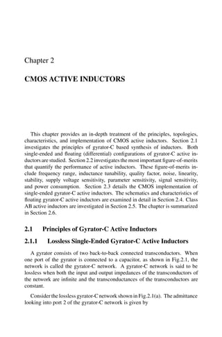
  • 1. Chapter 2 CMOS ACTIVE INDUCTORS This chapter provides an in-depth treatment of the principles, topologies, characteristics, and implementation of CMOS active inductors. Section 2.1 investigates the principles of gyrator-C based synthesis of inductors. Both single-ended and floating (differential) configurations of gyrator-C active in- ductors are studied. Section 2.2 investigates the most important figure-of-merits that quantify the performance of active inductors. These figure-of-merits in- clude frequency range, inductance tunability, quality factor, noise, linearity, stability, supply voltage sensitivity, parameter sensitivity, signal sensitivity, and power consumption. Section 2.3 details the CMOS implementation of single-ended gyrator-C active inductors. The schematics and characteristics of floating gyrator-C active inductors are examined in detail in Section 2.4. Class AB active inductors are investigated in Section 2.5. The chapter is summarized in Section 2.6. 2.1 Principles of Gyrator-C Active Inductors 2.1.1 Lossless Single-Ended Gyrator-C Active Inductors A gyrator consists of two back-to-back connected transconductors. When one port of the gyrator is connected to a capacitor, as shown in Fig.2.1, the network is called the gyrator-C network. A gyrator-C network is said to be lossless when both the input and output impedances of the transconductors of the network are infinite and the transconductances of the transconductors are constant. Consider the lossless gyrator-C network shown in Fig.2.1(a). The admittance looking into port 2 of the gyrator-C network is given by
  • 2. 22 CMOS Active Inductors Y = Iin V2 = 1 s C Gm1Gm2 . (2.1) Eq.(2.1) indicates that port 2 of the gyrator-C network behaves as a single-ended lossless inductor with its inductance given by L = C Gm1Gm2 . (2.2) Gyrator-C networks can therefore be used to synthesize inductors. These synthesized inductors are called gyrator-C active inductors. The inductance of gyrator-C active inductor is directly proportional to the load capacitance C and inversely proportional to the product of the transconductances of the transconductors of the gyrator. Also, the gyrator-C network is inductive over the entire frequency spectrum. It should also be noted that the transconductor in the forward path can be configured with a negative transconductance while the transconductor in the feedback path has a positive transconductance, as shown in Fig.2.1(b). Although the transconductors of gyrator-C networks can be configured in various ways, the constraint that the synthesized inductors should have a large frequency range, a low level of power consumption, and a small silicon area requires that these transconductors be configured as simple as possible. Fig.2.2 shows the simplified schematics of the basic transconduc- tors that are widely used in the configuration of gyrator-C active inductors. Common-gate, common-drain, and differential-pair transconductors all have a positive transconductance while the common-source transconductor has a negative transconductance. To demonstrate this, consider the common-gate transconductor. An increase in vin will lead to a decrease in iD. Because io = J − iD, io will increase accordingly. So the transconductance of the common-gate transconductor is positive. Similarly, for the differential-pair transconductor in Fig.2.2(d). An increase in vin will result in an increase in iD1. Since iD2 = J3 − iD1, iD2 will decrease. Further io = J2 − iD2, io will increase. The differential-pair transconductor thus has a positive transconduc- tance. 2.1.2 Lossless Floating Gyrator-C Active Inductors An inductor is said to be floating if both the terminals of the inductor are not connected to either the ground or power supply of the circuits containing the active inductor. Floating gyrator-C active inductors can be constructed in a similar way as single-ended gyrator-C active inductors by replacing single- ended transconductors with differentially-configured transconductors, as shown in Fig.2.3. Because
  • 3. Principles of Gyrator-C Active Inductors 23 I G Vm1 V 2 2 G Vm2 1 V1 C L 2 1 2 G Vm1 V 2 2 G Vm2 1 V1 C 2 1 in Iin (a) (b) Vin Vin Vin Iin L 2 Vin Iin or Figure 2.1. Lossless singe-ended gyrator-C active inductors. Gm1 and Gm2 are the transcon- ductances of transconductors 1 and 2, respectively, and C is the load capacitance at node 1. (a) Transconductor in the forward path has a positive transconductance while the transconductor in the feedback path has a negative transconductance; (b) Transconductor in the forward path has a negative transconductance while the transconductor in the feedback path has a positive transconductance. V + in1 = − gm1 sC (V + in2 − V − in2), V − in1 = gm1 sC (V + in2 − V − in2), Io2 = gm2(V + in1 − V − in1), (2.3) we have Io2 = − 2gm1gm2 sC (V + in2 − V − in2). (2.4) The admittance looking into port 2 of the gyrator-C network is given by
  • 4. 24 CMOS Active Inductors Vb vin io vin io vin io vin io Vb in io Vb v M1 M2 M1 M2 (a) (b) (c) (d) (e) J J J J3 J1 J2 J Figure 2.2. Simplifiedschematic of basic transconductors. (a) Common-source transconductor io = −gmvin; (b) Common-gate transconductor io = gmvin; (c) Common-drain (source follower) transconductor io = gmvin; (d,e) Differential-pair transconductors io = gmvin. Y = Iin V + in2 − V − in2 = 1 s 2C gm1gm2 . (2.5) Eq.(2.5) reveals port 2 of the gyrator-C network behaves as a floating inductor with its inductance given by L = 2C gm1gm2 . (2.6)
  • 5. Principles of Gyrator-C Active Inductors 25 C G V - V( )m1 2+ 2- G V - V( )m2 1+ 1- LC 2- 2+ 1+ 1- 2+ 2- IinVin Vin Io2 Io1 Figure 2.3. Lossless floating gyrator-C active inductors. Gm1 and Gm2 are the transconduc- tances of transconductors 1 and 2, respectively, and C is the load capacitance at nodes 1+ and 1-. Floating gyrator-C active inductors offer the following attractive advantages over their single-ended counterparts : (i) The differential configuration of the transconductors effectively rejects the common-mode disturbances of the network, making them particularly attractive for applications where both analog and digital circuits are fabricated on the same substrate. (ii) The level of the voltage swing of floating active inductors is twice that of the corresponding single-ended active inductors. 2.1.3 Lossy Single-Ended Gyrator-C Active Inductors When either the input or the output impedances of the transconductors of gyrator-C networks are finite, the synthesized inductors are no longer lossless. Also, the gyrator-C networks are inductive only in a specific frequency range. Consider the gyrator-C network shown in Fig.2.4 where Go1 and Go2 denote the total conductances at nodes 1 and 2, respectively. Note Go1 is due to the finite output impedance of transconductor 1 and the finite input impedance of transconductor 2. To simplify analysis, we continue to assume that the transconductances of the transconductors are constant. Write KCL at nodes 1 and 2 (sC1 + Go1)V1 − Gm1V2 = 0 (node 1), −Iin + (sC2 + Go2)V2 − Gm2(−V1) = 0, (node 2). (2.7) The admittance looking into port 2 of the gyrator-C network is obtained from
  • 6. 26 CMOS Active Inductors Y = Iin V2 = sC2 + Go2 + 1 s C1 Gm1Gm2 + Go1 Gm1Gm2 . (2.8) Eq.(2.8) can be represented by the RLC networks shown in Fig.2.4 with its parameters given by Rp = 1 Go2 , Cp = C2, Rs = Go1 Gm1Gm2 , L = C1 Gm1Gm2 . (2.9) G Vm1 CR R L p p s Go2 C2 V 2 2 G V1 V1 Go1 C1 m2 2 1 2 Iin Vin Iin Vin CR R L p p s 2 Iin Vin Figure 2.4. lossy single-ended gyrator-C active inductors. C1 and Go1, C2 and Go2 denote the total capacitances and conductances at nodes 1 and 2, respectively. We comments on the preceding results :
  • 7. Principles of Gyrator-C Active Inductors 27 When the input and output conductances of the transconductors are consid- ered, the gyrator-C network behaves as a lossy inductor with its parasitic parallel resistance Rp, parallel capacitance Cp, and series resistance Rs. Rp should be maximized while Rs should be minimized to low the ohmic loss. The finite input and output impedances of the transconductors of the gyrator-C network, however, have no effect on the inductance of the active inductor. Rp and Cp are solely due to Go2 and C2. Go1 and C1 only affect Rs and L. The resonant frequency of the RLC networks of the active inductor is given by ωo = 1 LCp = Gm1 C1 Gm2 C2 = √ ωt1ωt2, (2.10) where ωt1,2 = Gm1,2 C1,2 (2.11) is the cut-off frequency of the transconductors. ωo is the self-resonant frequency of the gyrator-C active inductor. This self-resonant frequency is typically the maximum frequency at which the active inductor operates. The self-resonant frequency of an active inductor is set by the cut-off frequency of the transconductors constituting the active inductor. The small-signal behavior of a gyrator-C active inductor is fully character- ized by its RLC equivalent circuit. The RLC equivalent circuit of gyrator-C active inductors, however, can not be used to quantify the large-signal behav- ior, such as the dependence of the inductance on the dc biasing condition of the transconductors and the maximum signal swing of the gyrator-C active inductors. When the conductances encountered at nodes 1 and 2 of the gyrator-C active inductors are zero (lossless), the phase of the impedance of the synthesized inductor is π 2 . However, when these conductances are non-zero, the phase of the impedance of the synthesized inductor will deviate from π 2 , giving rise to a phase error. The phase error is due to Rp and Rs of the active inductors. The phase of the impedance of practical active inductors should be made constant and to be as close as possible to π 2 .
  • 8. 28 CMOS Active Inductors The finite input and output impedances of the transconductors constituting active inductors result in a finite quality factor. For applications such as band-pass filters, active inductors with a large quality factor are mandatory. In these cases, Q-enhancement techniques that can offset the detrimental effect of Rp and Rs should be employed to boost the quality factor of the active inductors. 2.1.4 Lossy Floating Gyrator-C Active Inductors Lossy floating gyrator-C active inductors can be analyzed in a similar way as lossy single-ended gyrator-C active inductors. Consider the lossy floating gyrator-C network shown in Fig.2.5. We continue to assume that the transcon- ductances of the transconductors are constant. Writing KCL at nodes 1-, 1+, 2-, and 2+ yields −Gm1(V + 2 − V − 2 ) + sC1 + Go1 2 (V − 1 − V + 1 ) = 0, Iin + sC2 + Go2 2 (V − 2 − V + 2 + Gm2(V + 1 − V − 1 ) = 0, (2.12) The admittance looking into port 2 of the gyrator-C network is obtained from Y = Iin V + 2 − V − 2 = s C2 2 + Go2 2 + 1 s C1 2Gm1Gm2 + Go1 2Gm1Gm2 . (2.13) Eq.(2.12) can be represented by the RLC network shown in Fig.2.5 with its parameters given by Rp = 2 Go2 , Cp = C2 2 , Rs = Go1/2 Gm1Gm2 , L = C1/2 Gm1Gm2 . (2.14)
  • 9. Characterization of Active Inductors 29 The constant 2 in (2.14) is due to the floating configuration of the active inductor. The capacitance and conductance at the interface nodes 1+ and 1− and those at the internal nodes 2+ and 2− will become C2/2 and Go2/2, and C1/2 and Go21/2, respectively. Eq.(2.9) can be used to derive (2.14) without modification. G V - V( )m1 CR R L p p sGo2 C2 V 2 2 V1 2- 1- 2+ Go2 C2 Go1 C1 Go1 C1 1+ 2+ 2 -+ G V - V( )m2 1 1 -+ 2- Go2 C2 Go1 C1 Go1 C1C2 Go2 Iin Vin Iin Vin Figure 2.5. Lossy floating gyrator-C active inductors. C1 and Go1, C2 and Go2 represent the total capacitances and conductances at nodes 1 and 2, respectively. 2.2 Characterization of Active Inductors In this section, we investigate the most important figure-of-merits that pro- vide quantitative measures of the performance of active inductors. These figure-of-merits include frequency range, inductance tunability, quality factor, noise, linearity, stability, supply voltage sensitivity, parameter sensitivity, signal sensitivity, and power consumption. 2.2.1 Frequency Range It was shown in the preceding section that an lossless gyrator-C active induc- tor exhibits an inductive characteristic across the entire frequency spectrum. A lossy gyrator-C active inductor, however, only exhibits an inductive charac- teristic over a specific frequency range. This frequency range can be obtained by examining the impedance of the RLC equivalent circuit of the lossy active inductor
  • 10. 30 CMOS Active Inductors Z = Rs CpL s L Rs + 1 s2 + s 1 RpCp + Rs L + Rp + Rs RpCpL . (2.15) When complex conjugate poles are encountered, the pole resonant frequency of Z is given by ωp = Rp + Rs RpCpL . (2.16) Because Rp Rs, Eq.(2.16) is simplified to ωp≈ 1 LCp = ωo, (2.17) where ωo is the self-resonant frequency of the active inductor. Also observe that Z has a zero at frequency ωz = Rs L = Go1 C1 . (2.18) The Bod´e plots of Z are sketched in Fig.2.6. It is evident that the gyrator-C network is resistive when ω < ωz, inductive when ωz < ω < ωo, and capacitive when ω > ωo. The frequency range in which the gyrator-C network is inductive is lower-bounded by ωz and upper-bounded by ωo. Also observed is that Rp has no effect on the frequency range of the active inductor. Rs, however, affects the lower bound of the frequency range over which the gyrator-C network is inductive. The upper bound of the frequency range is set by the self resonant frequency of the active inductor, which is set by the cut-off frequency of the transconductors constituting the active inductor. For a given inductance L, to maximize the frequency range, both Rs and Cp should be minimized. 2.2.2 Inductance Tunability Many applications, such as filters, voltage or current controlled oscillators, and phase-locked loops, require the inductance of active inductors be tunable with a large inductance tuning range. It is seen from (2.9) that the inductance of gyrator-C active inductors can be tuned by either changing the load capacitance or varying the transconductances of the transconductors constituting the active inductors. Capacitance tuning in standard CMOS technologies is usually done by using varactors. Two types of varactors exists, namely pn-junction varactors
  • 11. Characterization of Active Inductors 31 90 -90 0 |Z(j )|w Z(j )w w w 45 deg./dec. -90 deg./dec. Inductive CapacitiveResistive 20 dB/dec. -20 dB/dec. w wz o w wz o (dB) (Degree) R R R +R s p ps Figure 2.6. Bod´e plots of the impedance of lossy gyrator-C active inductors. and MOS varactors. The sideviews of pn-junction varactors are shown in Fig.2.7 for p+/n-well junctions and Fig.2.8 for n+/p-well junctions. Because p-substrate is connected to the ground, n+/p-well varactors are single-ended. p+/n-well varactors, on the other hand, are floating varactors. The swing of the voltages at the nodes of the varactors must ensure that the n+/p-well and p+/n- well junctions be revise biased all the time such that a junction capacitance exists. The junction capacitance of an abrupt pn-junction is given by CJ = CJo 1 + vR φo , (2.19) where CJo is the junction capacitance at zero-biasing voltage, vR is the reverse biasing voltage of the junction and φo is built-in potential of the junction. It is seen that CJ varies with vR in a nonlinear fashion. The performance of junction varactors is affected by the following factors : Large parasitic series resistance - p+/n-well varactors suffer from a large series resistance - the resistance of the n-well. As a result, the quality factor of the varactor quantified by Q = 1 ωRn−wellC , (2.20)
  • 12. 32 CMOS Active Inductors where Rn−well is the parasitic series resistance, is small. To minimize this unwanted resistance, the spacing between p+ and n+ diffusions should be minimized. Large parasitic capacitance between n-well and p-substrate - The larger the capacitance of the varactors, the larger the n-well and subsequently the larger the n-well/p-substrate junction capacitance. Small capacitance tuning range - The nonlinear characteristics of CJ result in a small capacitance tuning range with a low capacitance tuning ratio. Stringent voltage swing requirement - As pointed out earlier that the p+/n- well and n+/p-well junctions must remain in a reverse biasing condition all the time to ensure the existence of a junction capacitance. This imposes a stringent constraint on the swing of the voltage across the terminals of the varactors p-substrate n-well p+ n+ Rn-well pn-junction 1 2 1 2 CJ CJ Rn-well D Figure 2.7. Sideview of p+/n-well varactors The sideview of accumulation-mode MOS varactors is shown in Fig.2.9 for VG < VS and Fig.2.10 for VG > VS. If VG < VS, the electrons in the n-well region underneath the gate will be repelled and a depletion region is created. When VG > VS, the electrons from the n+ diffusion regions will be pulled to the region underneath the gate, creating an accumulation layer and CGS arises to the gate-oxide capacitance. As pointed out in [68] that Cmax Cmin can be made from 2.5 to 3 when −1V ≤vGS≤1V . A key advantage of accumulation-mode MOS varactors is the large voltage swing across the terminals of the varactors. They are the most widely used varactors in voltage/current-controlled oscillators.
  • 13. Characterization of Active Inductors 33 p-substrate p-welln+ p+ Rp-well 1 2 1 2 CJ CJ Figure 2.8. Sideview of n+/p-well varactors. A common drawback of junction varactors and MOS varactors is their small capacitance tuning range. n-well n+ V GS V p-substrate n+ Depletion region Figure 2.9. Sideview of accumulation-mode MOS varactors when VG < VS. Conductance tuning can be done by varying the dc operating point of the transconductors. This approach offers a large conductance tuning range, subse- quently a large inductance tuning range. The conductance tuning range is set by the constraint that the transconducting transistors of the transconductors must remain in the saturation. Conductance tuning can be used for the coarse tuning of the inductance while capacitance tuning can be used for the fine tuning of the inductance, as shown in Fig.2.12. The conductance of either the transconductor
  • 14. 34 CMOS Active Inductors n-well n+ V GS V p-substrate n+ Gate voltage induced electrons Figure 2.10. Sideview of accumulation-mode MOS varactors when VG > VS. vGS Cmin Cmax CGS VGS Figure 2.11. Capacitance of accumulation-mode MOS varactors. with a positive transconductance or that with a negative transconductance can be tuned. The conductance tuning range is set by the pinch-off condition while the capacitance tuning range is set by the range of the control voltage of the varactors. It is seen from (2.9) that a change in the transconductances of the transcon- ductors of an active inductor will not affect Rp and Cp of gyrator-C active inductors. It will, however, alter the parasitic series resistance Rs of the active inductor. This is echoed with a change in the quality factor of the active induc- tors. The variation of the quality factor due to the tuning of L must therefore be compensated for such that L and Q are tuned in a truly independent fashion. It should be noted that the fine tuning of the inductance of active inductors from the capacitance tuning does not affect Rs.
  • 15. Characterization of Active Inductors 35 G Vm1 2 -G Vm2 1 C 2 1 C x Vin Figure 2.12. Inductance tuning of gyrator-C active inductors. Conductance tuning can be carried out by varying either Gm1 or Gm2 while capacitance tuning is done by varying the varactor Cx. 2.2.3 Quality Factor The quality factor Q of an inductor quantifies the ratio of the net magnetic energy stored in the inductor to its ohmic loss in one oscillation cycle. For spiral inductors, the quality factor of these inductors is independent of the voltage / current of the inductors. This property, however, does not hold for active inductors as the inductance of these inductors depends upon the transconductances of the transconductors constituting the active inductors and the load capacitance. When active inductors are used in applications such as LC oscillators, the inductance of the active inductors is a strong function of the swing of the voltage and current of the oscillators. To quantify the ratio of the net magnetic energy stored in the inductor to its ohmic loss in one oscillation cycle and relate it to the performance of LC oscillators, in particular, the phase noise of the oscillators, an alternative definition of the quality factor that accounts for the swing of the voltage / current of the active inductors is needed. Instantaneous Quality Factor The quality factor Q of an inductor quantifies the ratio of the net magnetic energy stored in the inductor to its ohmic loss in one oscillation cycle [33, 29] Q = 2π× Net magnetic energy stored Energy dissipated in one oscillation cycle . (2.21) For a linear inductor, the complex power of the active inductor is obtained from P(jω) = I(jω)V ∗ (jω) = e[Z]|I(jω)|2 + j m[Z]|I(jω)|2 , (2.22)
  • 16. 36 CMOS Active Inductors where e[Z] and m[Z] are the resistance and inductive reactance of the inductor, respectively, V (jω) and I(jω) are the voltage across and the current through the inductor, respectively, the superscript ∗ is the complex conjugation operator, and |.| is the absolute value operator. The first term in (2.22) quantifies the net energy loss arising from the parasitic resistances of the inductor, whereas the second term measures the magnetic energy stored in the inductor. Eq.(2.21) in this case becomes Q = m[Z] e[Z] . (2.23) Eq.(2.23) provides a convenient way to quantify Q of linear inductors including active inductors. Active inductors are linear when the swing of the voltages / currents of the inductors are small and all transistors of the active inductors are properly biased. The quality factor of a lossy gyrator-C active inductor can be derived directly from (2.15) and (2.23) Q = ωL Rs Rp Rp + Rs 1 + ωL Rs 2 1 − R2 sCp L − ω2 LCp . (2.24) Fig.2.13 shows the frequency dependence of the quality factor of the active inductor with Rs = 4Ω, Rp = 1kΩ, Cp = 140 fF, and L = 1.6 nH [33]. It is seen that the first term in (2.24), denoted by Q1 = ωL Rs , (2.25) quantifies the quality factor of the active inductor at low frequencies. The second term, denoted by Q2 = Rp Rp + Rs 1 + ωL Rs 2 , (2.26) accounts for the effect of the finite output impedance of deep sub-micron MOSFETs, whereas the third term, denoted by Q3 = 1 − R2 sCp L − ω2 LCp, (2.27)
  • 17. Characterization of Active Inductors 37 10 8 10 9 10 10 10 11 0 1 2 3 4 5 6 7 8 9 10 Ferquency [Hz] Qualityfactor Q 1 (ω) Q 2 (ω) Q 3 (ω) Q(ω) Figure 2.13. Frequency dependence of the quality factor of active inductors. shows that the quality factor vanishes when frequency approaches the cut-off frequency of the transconductors of the active inductor. Q2 and Q3 manifest themselves at high frequencies only. The sensitivity of the quality factor of the active inductor with respect to Rs and Rp is investigated in Figs.2.14 and 2.15, respectively. It is seen that Q1 dominates the quality of the active inductor and is therefore widely used to quantify the quality factor of active inductors. To boost the quality factor of active inductors, Rs must be minimized. Four approaches can be used to reduce Rs: Approach 1 - Because Rs = Go1 Gm1Gm2 , Rs can be lowered by reducing Go1 directly. Since Go1 is typically the output impedance of the transcon- ductor with a positive transconductance, the use of transconductors with a large output impedance is critical. As an example, consider the transcon- ductors shown in Fig.2.16. The transconductance of the transconductor in Fig.2.16(a) is positive. This is because an increase in vin will lead to an increase in vGS, which in turn increases iD. Because io = iD − J, io will increase as well. The transconductance of the transconductor in Fig.2.16(b) is also positive. This is because an increase in vin will decrease iD1. As a result, iD2 = J1 − iD1 will increase. Since io = iD2 − J2, io will increase as well. Although both transconductors have a positive transcon-
  • 18. 38 CMOS Active Inductors 10 8 10 9 10 10 10 11 0 5 10 15 Ferquency [Hz] Qualityfactor Rs =1Ω Rs =10Ω Figure 2.14. The effect of Rs on the quality factor of active inductors. Rs is varied from 1Ω to 10Ω with step 1Ω. ductance and both have an infinite input impedance, the output impedance of the transconductor in Fig.2.16(a) is given by 1 gm approximately whereas that of the transconductor in Fig.2.16(b) is given by ro2. Active inductors constructed using the transconductor in Fig.2.16(b) will have a smaller Rs, subsequently a higher Q. Approach 2 - Rs can be lowered by increasing Gm1 and Gm2 directly. Since the transconductances of the transconductors are directly proportional to the dc biasing currents and the width of the transistors of the transconductors, Rs can be lowered by either increasing the dc biasing currents or increasing the transistor width. The former, however, increases the static power con- sumption of the active inductors whereas the latter lowers the self-resonant frequency of the active inductors. Another downside of this approach is that the inductance of the inductors L will also be affected. Approach 3 - Reduce Go1 using advanced circuit techniques, such as cas- codes. Cascodes are effective in lowering the output conductance and can be used here to reduce Go1, as shown in Fig.2.17. Table 2.1 compares the minimum supply voltage and output conductance of basic, cascode, regulated cascode, and multi-regulated cascode transconductors.
  • 19. Characterization of Active Inductors 39 10 8 10 9 10 10 10 11 0 1 2 3 4 5 6 7 8 9 10 Ferquency [Hz] Qualityfactor R p =1 kΩ R p =10 kΩ Figure 2.15. The effect of Rp on the quality factor of active inductors. Rp is varied from 1kΩ to 10kΩ with step 1kΩ. M1 M2 Vb v in v in io io (a) (b) J J J 1 2 M1 M2 Vbv in io (c) J J 1 2 Figure 2.16. Simplified schematics of transconductors with a positive transconductor. (a) Common-drain transconductor; (b,c) Differential-pair transconductors. Approach 4 - Use a shunt negative resistor at the output of the positive transconductor to cancel out the parasitic resistances, both series and par- allel, of active inductors. It is well known that the series RL network of the RLC network shown in Fig.2.18 can be replaced with the parallel RL network shown in the figure with [68]
  • 20. 40 CMOS Active Inductors M1v M1 M2 M1 M2 in Vb (a) (b) (c) M2Vb M1vin (d) i o i o i o i o vin vin vin vo -A vin vo -AM3 M3 M4 Figure 2.17. Simplified schematics of cascode transconductors. (a) Basic transconductor; (b) Cascode transconductor; (c) Regulated cascode transconductor; (d) Multi-regulated cascode transconductor. Rp = Rs(1 + Q2) Lp = Ls 1 + 1 Q2 , (2.28) where Q = ωLs Rs . This is because in order to have the two network to be equivalent, in other words, to exhibit the same terminal impedance, Zs(jω) = Zp(jω) is required. Rs + jωLs = jωRpLp Rp + jωLp . (2.29) Matching the real and imaginary parts yield
  • 21. Characterization of Active Inductors 41 Table 2.1. The minimum supply voltage and output conductance of basic and cascode transcon- ductors. Transconductor Min. VDD Output impedance Basic 2Vsat Go = 1 ro Cascode 3Vsat Go = 1 ro1(ro2gm2) Regulated cascode 2VT + Vsat Go = 1 ro1(ro2gm2)(ro3gm3) Multi-regulated cascode 2VT + Vsat Go = 1 ro1(ro2gm2)(ro3gm3)(ro4gm4) . RsRp − ω2LsLp = 0, RsLp + RpLs = RpLp. (2.30) Eq.(2.28) follows from Eq.(2.30). Note that (2.28) is valid at all frequencies. R L s Z R L p p s Z s pC C Figure 2.18. Transformation of a RL parallel branch to a RL series branch. Now consider the RLC network of an active inductor shown in Fig.2.19. The L ∼ Rs branch of the RLC circuit of the active inductor is replaced with the parallel ˆL ∼ ˆRp network with ˆL = L 1 + 1 Q2 , ˆRp = Rs(1 + Q2 ). (2.31)
  • 22. 42 CMOS Active Inductors Consider two cases : – Case 1 - If Rs is negligible, the quality factor of the active inductor is mainly determined by Rp. From (2.24) with Rs = 0, we arrive at Q = Rp ωL 1 − ω ωo 2 . (2.32) At frequencies below ωo, ω ωo 2 ≈0 and Q≈ Rp ωLs (2.33) follows. – Case 2 - If Rp is large, the quality factor is mainly determined by Rs Q = ωL Rs 1 − ωz ωo 2 − ω ωo 2 . (2.34) At frequencies above ωz and below ωo, ωz ωo 2 ≈0 and ω ωo 2 ≈0. Eq.(2.34) is simplified to Q≈ ωL Rs . (2.35) As shown in Fig.2.19, the total parasitic parallel resistance of the active inductor becomes Rtotal = Rp// ˆRp. (2.36) In this case, a negative resistor of resistance Rcomp = −Rtotal can be con- nected in parallel with Cp to eliminate the effect of both Rp and Rs of the active inductor simultaneously. Note that the resistance of the negative re- sistor should be made tunable such that a total cancellation can be achieved. The quality factor of the compensated active inductor at ωo is given by Q(ωo) = (Rp|| ˆRp||Rcomp) Cp + Ccomp ˆL , (2.37)
  • 23. Characterization of Active Inductors 43 where Ccomp is the input capacitance of the compensating negative resistor. It should be noted that because Rs and Rp are frequency-dependent, Rcomp should be designed in such a way that a total resistance cancellation is achieved across the frequency range of the active inductor. It should also be noted that although the negative resistor compensation technique is widely used to improve the quality factor of spiral inductors, a total compensation in this case is difficult to achieve. This is because an active negative resistor is used to cancel out the largely skin-effect induced parasitic series resistance of spirals. CR R L p p s CR R Lp p p Rcomp Ccomp Figure 2.19. Q enhancement using a shunt negative resistor. Average Quality Factors Active inductors are RLC tanks when Rs, Rp, and Cp are accounted for. The quality factor of LC tanks is obtained from [69] Q(ω) = ωo 2 ∂φ(ω) ∂ω , (2.38) where φ(ω) is the phase of the tank impedance. The quality factor of a passive LC tank at a given frequency is independent of the current of the tank. Unlike passive LC tanks, the inductance of the active inductors varies with the current / voltage of the inductors. The effective quality factor defined as Q(ω) = ω 2(Imax − Imin) Imax Imin Q(ω, i)di, (2.39) where Imin and Imax are the minimum and maximum currents of the transcon- ductors of active inductors, and Q(ωo, i) is the instantaneous quality factor at frequency ω and channel current i provides an effective mean to quantify the quality factor of active inductors, especially when active inductors are em- ployed in circuits that are operated in a large-signal mode, such as LC tank oscillators.
  • 24. 44 CMOS Active Inductors 2.2.4 Noise Active inductors exhibit a high level of noise as compared with their spiral counterparts. To analyze the noise of a gyrator-C active inductor, the power of the input-referred noise-voltage and that of the noise-current generators of the transconductors constituting the active inductor must be derived first. Fig.2.20 shows the partial schematics of basic transconductors widely used in the construction of gyrator-C active inductors. The power of the input-referred noise-voltage generator, denoted by v2 n, and that of the input-referred noise- current generator, denoted by i2 n, of these transconductors can be derived using conventional noise analysis approaches for 2-port networks [70], and the results are given in Table 2.2 where i2 nD = 4kT(γ + Rggm)gmΔf (2.40) represents the sum of the power of the thermal noise generated in the channel of MOSFETs and the thermal noise of the gate series resistance of MOSFETs, Rg is the gate series resistance, γ = 2.5 for deep sub-micron devices, T is the temperature in degrees Kelvin, and k is Boltzmann constant. The effect of the flicker noise of MOSFETs, which has a typical corner frequency of a few MHz [71], is neglected. The thermal noise of other parasitics of MOSFETs, such as the thermal noise of the bulk resistance of the source and drain diffusions, is also neglected. To illustrate how the results of Table 2.2 are derived, consider the common- gate transconductor. To derive the input-referred noise-voltage generator v2 n of the transconductor, we first short-circuit the input of the transconductor, as shown in Fig.2.21. The output noise power of the transconductor due to inD is calculated v2 no = r2 oi2 nD, (2.41) where ro is the output resistance of the transistor. We then remove i2 nD and apply vn at the input of the transconductor, as shown in Fig.2.22. The output noise power of the transconductor is obtained v2 no = (1 + gmro)2 v2 n. (2.42) Equating (2.41) and (2.42) yields v2 n = r2 o (1 + gmro)2 i2 nD≈ 1 g2 m i2 nD. (2.43)
  • 25. Characterization of Active Inductors 45 Common source Cascode Common gate Source follower Transconductors with noise sources Transconductors with noise generators Figure 2.20. Input-referred noise-voltage and noise-current generators of transconductors at low frequencies.
  • 26. 46 CMOS Active Inductors Table2.2. Powerofinput-referrednoise-voltageandnoise-currentgenerators ofbasictranscon- ductors at low frequencies. Transconductor v2 n i2 n Common source v2 n = i2 nD g2 m i2 n = 0 Cascode v2 n = i2 nD1 g2 m1 + i2 nD2 (gm1ro1gm2)2 i2 n = 0 Common gate v2 n = i2 nD g2 m i2 n = 0 Source follower v2 n = i2 nD g2 m i2 n = 0 g vm gs ro vin inDvgs Vb inD 2 vno Figure 2.21. Derivation of input-referred noise-voltage generator of a common-gate transcon- ductor at low frequencies. Note that we have utilized rogm 1 in (2.43) to simplify the results. To derive the noise-current generator of the common-gate transconductor, consider Fig.2.23 where the input port of the transconductor is open-circuited and the output noise power of the circuit is calculated. To avoid the difficulty caused by the floating node 1, we assume that there exists a resistor of resistance
  • 27. Characterization of Active Inductors 47 g vm gs ro vn vgsVb vn vno Figure 2.22. Derivation of the input-referred noise-voltage generator of a common-gate transconductor at low frequencies. g vm gs ro vin inDvgs Vb inD 2 vno Rx 1 2 Figure 2.23. Derivation of the input-referred noise-current generator of a common-gate transconductor at low frequencies. Rx between node 1 and the ground. Note that this approach is used in most IC CAD systems to avoid floating nodes. Writing KCL at nodes 1 and 2 yields (gx + gm + go)v1 − gov2 = inD (node 1), −(go + gm)v1 + gov2 + inD = 0 (node 2). (2.44) Solving (2.44) yields v2 2 = 1 g2 o i2 nD. (2.45)
  • 28. 48 CMOS Active Inductors We then apply the noise-current generator in at the input of the circuit, remove all the noise sources of the circuit, as shown in Fig.2.24, and compute the output noise power. Writing KCL at nodes 1 and 2 yields (gx + gm + go)v1 − gov2 + in = 0 (node 1), −(go + gm)v1 + gov2 = 0 (node 2). (2.46) Solving (2.46) yields v2 2 = 1 + gm go 2 1 g2 x i2 n. (2.47) Equating (2.45) and (2.47) yields i2 n = gx go 2 i2 nD 1 + gm go 2 . (2.48) Taking the limit Rx→∞ or equivalently gx→0 in (2.48), we arrive at i2 n = 0. (2.49) g vm gs ro i n vgs Vb i n vno Rx 1 2 Figure 2.24. Derivation of the input-referred noise-current generator of a common-gate transconductor at low frequencies. Once v2 n and i2 n of the transconductors are available, the power of the input- referred noise-voltage and noise-current generators of active inductors can be derived.
  • 29. Characterization of Active Inductors 49 Consider the active inductor of Fig.2.25(a) where v2 n1 and v2 n2 denote the power of the noise-voltage generators of the transconductors 1 and 2, respec- tively, and Y1 and Y2 are the admittance at ports 1 and 2, respectively. For the network of Fig.2.25(a), it is trivial to show that V 2 1 = Vn1 + Y1 Gm2Vn2 + Y2Vn1 Y1Y2 + Gm1Gm2 2 . (2.50) For the network of Fig.2.25(b), we have V 2 1 = Vn + Y1 Y1Y2 + Gm1Gm2 In 2 . (2.51) To ensure that Fig.2.25(a) and Fig.2.25(b) are equivalent, the right hand-side of (2.50) and that of (2.51) must be the same. To achieve this, we impose Vn = Vn1, In = Y2Vn1 + Gm2Vn2. (2.52) Because Zin(s) = Y1 Y1Y2 + Gm1Gm2 , (2.53) we arrive at Vn = Vn1 + ZinIn. (2.54) For lossy gyrator-C active inductors, we have Y1 = Go1 + sC1, Y2 = Go2 + sC2, (2.55) Eq.(2.52) becomes Vn = Vn1, In = (Go2 + sC2)Vn1 + Gm2Vn2. (2.56)
  • 30. 50 CMOS Active Inductors By assuming Vn1 and Vn2 are uncorrelated, we arrive at V 2 n = V 2 n1, I2 n = Go2 + jωC2 2 V 2 n1 + G2 m2V 2 n2. (2.57) G Vm1 + G Vm2 - G Vm1 + G Vm2 - v n1 v n2 v n in 2 1 2 1 YY2 1 Y1Y2 Figure 2.25. Noise of single-ended gyrator-C active inductors. 2.2.5 Linearity The preceding development of gyrator-C active inductors assumes that the transconductors of the active inductors are linear. This assumption is only valid if the swing of the input voltage of the transconductors is small. When the voltage swing is large, the transconductors will exhibit a nonlinear charac- teristic and the synthesized active inductors are no longer linear. The linearity constraint of active inductors sets the maximum swing of the voltage of the active inductors. If we assume that the transconductances of the transistors of gyrator-C active inductors are constant when the transistors are biased in the saturation, then the maximum swing of the voltage of the active inductors can be estimated from the pinch-off condition of the transistors. When the transistors of active inductors enter the triode region, the transconductances of the transistors decrease from gm (saturation) to gds (triode) in a nonlinear fashion, as illustrated graphically in Fig.2.26. It should be emphasized that although the transconductances of the transconductors of gyrator-C networks drop when the operating point of the transistors of the transconductors moves from the saturation region to the triode region, the inductive characteristics at port 2 of the gyrator-C network remain. The inductance of the gyrator-C active inductors, however, increases from L = C Gm1Gm2 to L = C Gds1Gds2 , where Gm1,m2 are the transconductances of transconductors 1 and 2 respectively when (b)(a)
  • 31. Characterization of Active Inductors 51 in the saturation and Gds1,ds2 are the transconductances of transconductors 1 and 2 respectively when in the triode. Note that we have assumed the load capacitance C remains unchanged. The inductance thus varies with the swing of the voltage of the active inductors in a nonlinear fashion. It should also be noted that the parasitic resistances of active inductors also vary with the voltage swing of the active inductors. VGS1 VGS2 i DS vDS DiDS1 DiDS2 DiDS1 DVGS g =m DiDS2 DVGS g =ds Pinch-off VDS1VDS2 Figure 2.26. Transconductance of MOSFETs in the saturation and triode regions. Because ΔiDS1 > ΔiDS2, gm > gds follows. 2.2.6 Stability Gyrator-C active inductors are negative feedback systems. The stability of active inductors is critical to the overall stability of systems employing active inductors. In this section, we investigate the stability of gyrator-C active inductors. The impedance looking into port 2 of the gyrator-C active inductor shown in Fig.2.4 is given by Z = sC1 + Go1 s2C1C2 + s(C1 + C2) + Gm1Gm2 , (2.58) where we have utilized Gm Go to simply the results. The poles of the system are given by p1,2 = C1 + C2 2C1C2 − 1± 1 − 4C1C2Gm1Gm2 (C1 + C2)2 . (2.59)
  • 32. 52 CMOS Active Inductors The poles of the gyrator-C active inductor are located in the left half of the s-plane and the gyrator-C active inductor is a stable system. The degree of stability can be assessed by evaluating its damping factor, which is obtained by comparing the denominator of (2.58) with the standard form of the characteristic equation of second-order systems s2 + 2ωoξs + ω2 o = 0, (2.60) where ξ denotes the damping factor and ωo is the pole resonant frequency. The result is given by ξ = 1 2 √ Gm1Gm2 C2 C1 + C1 C2 . (2.61) Eq.(2.61) reveals that an increase in Gm1 and Gm2 will lead to a decrease in ξ. This is echoed with an increase in the level of oscillation in the response of the active inductor. Also observed from (2.61) is that the ratios C1 C2 and C2 C1 have a marginal impact on the damping factor simply because these two quantities vary in the opposite directions when C1 and C2 change, and the values of C1 and C2 are often close. If C1 = C2 = C and Gm1 = Gm2 = Gm, we have p1,2 = 1 C − 1± 1 − G2 m , ξ = 1 Gm . (2.62) An increase of Gm will lead to a decrease of ξ. This is echoed with a reduced level of damping. Because e[p1,2] = − 1 C , the absolute stability margin is set by the capacitance C and is independent of Gm. It should be noted that the preceding analysis is based on the assumption that active inductors are 2nd-order systems. When the parasitics of MOSFETs are accounted for, active inductors are no longer 2nd-order systems and their stability will deteriorate. 2.2.7 Supply Voltage Sensitivity The supply voltage sensitivity of the inductance of active inductors is a figure-of-merit quantifying the effect of the variation of the supply voltage on the inductance of the active inductors. The fluctuation of the supply voltage of a mixed analog-digital system is mainly due to the switching noise of the system
  • 33. Characterization of Active Inductors 53 [14]. Assume that the supply voltage of a mixed-mode system containing an active inductor varies from VDD and VDD + ΔVDD, where ΔVDD is a random variable with E[ΔVDD] = 0, where E[.] denotes the mathematical mean operator. For a well designed mixed-mode system, ΔVDD VDD holds. The small-signal analysis approach can therefore be employed to analyze the effect of ΔVDD on the inductance of the active inductor. Following the definition of normalized sensitivity given in [72], the normalized sensitivity of the inductance of an active inductor to the supply voltage is defined as SL VDD = VDD L ∂L ∂VDD . (2.63) The fluctuation of the supply voltage VDD affects the inductance of the active inductor mainly by altering the dc operating point, subsequently the transconductances of the transconductors constituting the active inductor. By assuming that the load capacitance C of the gyrator-C active inductor does not vary with VDD and because L = C Gm1Gm2 , we arrive at ∂L ∂VDD = −L 1 Gm1 ∂L Gm1 + 1 Gm2 ∂L Gm2 . (2.64) The normalized supply voltage sensitivity of the active inductor is given by SL VDD = − SGm1 VDD + SGm2 VDD , (2.65) where SGm1 VDD and SGm2 VDD are the normalized supply voltage sensitivity of Gm1 and Gm2, respectively. Eq.(2.65) reveals that both SGm1 VDD and SGm2 VDD contribute equally to SL VDD . To minimize the supply voltage sensitivity of active inductors, transconductors with a constant Gm should be used. 2.2.8 Parameter Sensitivity The minimum feature size of MOS devices in modern CMOS technologies has been scaled down more aggressively as compared with the improvement in process tolerance such that the effect of process variation on the characteristics of circuits becomes increasingly critical. For example, the resistance of poly re- sistors in a typical 0.18μm CMOS process has an error of ±20% approximately and that of n-well resistors has an error of ±30% approximately. Analysis of the effect of parameter spread is vital to ensure that the performance of circuits meets design specifications once the circuits are fabricated. Active inductors consist of a number of active devices and their performance is greatly affected
  • 34. 54 CMOS Active Inductors by the parameter spread of these components. The normalized sensitivity of the inductance of an active inductor to a parameter xj of the inductor defined as SL xj = xj L ∂L ∂xj (2.66) quantifies the effect of the variation of the parameter xj on the inductance of the active inductor. By assuming that the parameters of the active inductor are Gaussian distributed and uncorrelated, the overall effect of the variation of the parameters of the active inductor on the inductance of the inductor is obtained from σ2 L = N j=1 ∂L ∂xj 2 σ2 xj , (2.67) where σL and σxj denote the standard deviations of L and xj, respectively, and N is the number of the parameters of the active inductor. For a gyrator-C active inductor, because ∂L C = 1 Gm1Gm2 , ∂L Gm1 = − C G2 m1Gm2 , ∂L Gm2 = − C Gm1G2 m2 , (2.68) we obtain the normalized spread of the inductance of the active inductor σ2 L L2 = σ2 C C2 + σ2 Gm1 G2 m1 + σ2 Gm2 G2 m2 . (2.69) There are two ways in which circuit designers can analyze the effect of parameter spread on the inductance of active inductors, namely worst-case analysis, also known as corner analysis, and Monte Carlo analysis. The former determines the inductance of active inductors at process corners while the latter quantifies the degree of the spread of the inductance of active inductors around the nominal inductance of the inductors. The accuracy of Monte Carlo analysis increases with an increase in the number of simulation runs and is therefore
  • 35. Implementation of Single-Ended Active Inductors 55 extremely time consuming. Corner analysis, on the other hand, is time-efficient but the results obtained from corner analysis are typically over conservative. Despite of this, corner analysis is the most widely used method to quantify the effect of process spread. 2.2.9 Signal Sensitivity Unlike spiral inductors whose inductance is independent of the voltage and current of the inductors, the inductance of gyrator-C active inductors varies with the voltage and current of the transconductors constituting the active inductors. This is because the transconductances Gm1 and Gm2 of the transconductors are signal dependent when signal swing is large. When an active inductor is used in applications where the voltage of the active inductor experiences a large degree of variation, such as active inductor LC oscillators, the transconductances of the transconductors of the active inductor vary with the signal swing. As a result, the inductance, parasitic resistances, and quality factor of the active inductor all vary with the signal swing. 2.2.10 Power Consumption Spiral inductors do not consume static power. Gyrator-C active inductors, however, consume dc power, mainly due to the dc biasing currents of their transconductors. The power consumption of gyrator-C active inductors them- selves is usually not of a critical concern because the inductance of these inductors is inversely proportional to the transconductances of the transcon- ductors constituting the inductors. To have a large inductance, Gm1 and Gm2 are made small. This is typically achieved by lowering the dc biasing currents of the transconductors. When replica-biasing is used to minimize the effect of supply voltage fluctuation on the inductance of active inductors, as to be seen shortly, the power consumed by the replica-biasing network must be accounted for. Also, when negative resistors are employed for boosting the quality factor of active inductors, their power consumption must also be included. Often the power consumption of an active inductor is set by that of its replica-biasing and negative resistor networks. 2.3 Implementation of Single-Ended Active Inductors The need for a high self-resonant frequency of active inductors requires that the transconductors of these active inductors be configured as simple as possible. This also lowers their level of power consumption and reduces the silicon area required to fabricate the inductors. Most reported gyrator-C active inductors employ a common-source configuration as negative transconductors, common-gate, source follower, and differential pair configurations as positive
  • 36. 56 CMOS Active Inductors transconductors. These basic transconductors have the simplest configurations subsequently the highest cutoff frequencies and the lowest silicon consumption. The load capacitor of the transconductors is realized using the intrinsic capacitance Cgs of the transistors of the transconductors directly to maximize the upper bound of the frequency range of the active inductors and to avoid the use of expensive floating capacitors, which are available only in mixed-mode CMOS processes. MOS varactors are often added in parallel with Cgs to tune the inductance of active inductors. This section presents a comprehensive treatment of both the circuit imple- mentation and characteristics of CMOS active inductors. To simplify analysis, the following assumptions are made in analysis of active inductors and in de- termination of both their signal swing and the minimum supply voltage : (i) nMOS and pMOS transistors have the same threshold voltage VT . (ii) nMOS and pMOS transistors have the same pinch-off voltage Vsat. (iii) Only Cgs is considered. Cgd and parasitic diffusion capacitances are neglected unless oth- erwise noted explicitly. (iv) The minimum voltage drop across biasing current sources and current-source loads is Vsat. 2.3.1 Basic Gyrator-C Active Inductors Fig.2.27 show the schematic of two basic gyrator-C active inductors. In Fig.2.27(a), the transconductor with a positive transconductance is common- gate configured while the transconductor with a negative transconductance is common-source configured. In Fig.2.27(b), the transconductor with a positive transconductance is common-drain configured while the transconductor with a negative transconductance is common-source configured. All transistors are biased in the saturation. A notable advantage of the active inductor in Fig.2.27(b) is that all transistors are nMOS, making it attractive for high- frequency applications. For Fig.2.27(a), we have C1 = Cgs2, Go1≈go1, Gm1 = gm1, C2 = Cgs1, Go2≈gm1, and Gm2 = gm2, where goj and gmj, j = 1, 2, are the output conductance and transconductance of transistor j, respectively. Using (2.9), we obtain the parameters of the equivalent RLC network of the active inductor
  • 37. Implementation of Single-Ended Active Inductors 57 Cp = Cgs1, Rp = 1 gm1 , L = Cgs2 gm1gm2 , Rs = go1 gm1gm2 . (2.70) M2 M1V M2 M1 (a) (b) b J2 J1 vin vin J1 J2 1 2 2 1 Figure 2.27. Simplified schematic of basic gyrator-C active inductors. It is observed from (2.70) that the parasitic parallel resistance Rp is rather small, limiting the quality factor of the active inductor. Also, the parasitic series resistance is large, further lowering the quality factor. In evaluating the quality factor of this active inductor, the effect of the parasitic series resistance Rs is often neglected as Rp is small. In this case, the quality factor of the active inductor is obtained from Q≈ Rp ωL = ωt2 ω . (2.71) The self-resonant frequency of the active inductor is given by ωo≈ 1 LCp = √ ωt1ωt2, (2.72) where
  • 38. 58 CMOS Active Inductors ωtj = gmj Cgsj , i = 1, 2 (2.73) is the cutoff frequency of transconductor j. At the self-resonance frequency of the active inductor ωo = √ ωt1ωt2, the quality factor becomes Q(ωo) = ωt2 ωt1 . (2.74) The frequency of the zero of the active inductor, which is the lower bound of the frequency range of the active inductor, is given by (2.18) ωz = go1 Cgs2 . (2.75) Eqs.(2.72) and (2.75) reveal that : In order to maximize the frequency range of the active inductor, ωz should be minimized. This can be achieved by reducing go1 or increasing Cgs2. The former is usually preferred as the latter lowers ωo. Because the output impedance of deep sub-micron MOSFETs is small. The detrimental effect of Rp = 1 gm1 on the quality factor of the active inductor can not be neglected. The effect of Rp, however, can be eliminated by connecting a negative resistor of resistance ˆRp = −Rp in parallel with Rp. gmVin Io Cin Vb M2 M1 vin J2 J1 vin (a) (b) Figure 2.28. Single-ended negative impedance networks. (a) Block diagram. (b) Circuit implementation.
  • 39. Implementation of Single-Ended Active Inductors 59 Negative resistors can be realized using transconductors with positive feed- back, as shown in Fig.2.28 for single-ended negative resistors and Fig.2.29 for differential negative resistors. The positive feedback of the single-ended negative resistor in Fig.2.28 is depicted as the followings : An increase in the gate voltage of M1 will increase the voltage at the source of M1. Since M2 is a common-gate configuration, an increase in the source voltage of M2 will increase the drain voltage of M2. A positive feedback is thus estab- lished. Readers can verify the positive feedback of the differential negative resistors of Fig.2.29 in a similar manner. For Fig.2.29. It can be shown that the impedance at low frequencies is given by Z≈ − 1 gm1 + 1 gm2 . (2.76) To maximize the frequency range over which a constant negative resistance exists, transconductors synthesizing negative resistors should be configured as simple as possible. Io + Io - Vin gmCin vin M1 M2 J vin (a) (b) vin M1 M2 J Figure 2.29. Differential negative impedance networks. (a) Block diagram. (b) Circuit imple- mentation. The tail current source in the differential configuration can be removed, provided that biasing currents are provided by the circuit connected to the negative resistor. Note that the removal of the biasing tail current source will also remove the tunability of the resistance of the negative resistor. The effect of Rs can be compensated for in three different ways : – Use cascodes and regulated cascodes to reduce go1 [37, 38, 65, 73]. It is well known that cascodes and regulated cascodes are effective means to boost the output impedance of transconductors. The price paid, however, is the reduced signal swing. – The reason that the preceding basic active inductors have a low Rp is because the input impedance of the positive transistor in Fig.2.27(a)
  • 40. 60 CMOS Active Inductors is 1/gm1 and the output impedance of the positive transconductor in Fig.2.27(b) is 1/gm2. The use of transconductors that have both a large output impedance and a large input impedance will eliminate this drawback. As an example, the differentially-configured posi- tive transconductor of Karsilayan-Schaumann active inductors shown in Fig.2.16(b,c) has an infinite input impedance and a large output impedance ro2 [74, 75, 48, 49, 61]. – Because the series RL branch of the RLC equivalent network of the active inductor can be replaced with a parallel ˆRˆL branch. The induc- tance of the parallel ˆRˆL branch is given by ˆL = L 1 + 1 Q2 while the resistance is given by ˆRp = (1 + Q2)Rs. The total parasitic parallel resistance of the active inductor becomes Rp,total = Rp|| ˆRp. The qual- ity factor of the active inductor can be made infinite theoretically by employing a shunt negative resistor whose resistance is −Rp,total. Table 2.3 compares the range of the voltage swing and the minimum supply voltage of the two basic active inductors. It is seen that the active inductor in Fig.2.27(a) offers a large input voltage swing and requires a lower minimum supply voltage. Table 2.3. Comparison of the input voltage swing and the minimum supply voltage of the basic active inductors in Fig.2.27. Active inductor Fig.2.27(a) Fig.2.27(b) Max. input voltage VDD − VT − Vsat VDD − VT − Vsat Min. input voltage Vsat VT Min. VDD VT + 2Vsat 2VT + Vsat 2.3.2 Wu Current-Reuse Active Inductors Fig.2.30 show the schematic of Wu current-reuse active inductors proposed in [42, 45, 36]. In the nMOS version of the active inductor, the positive transconductor is common-gate configured while the negative transconductor is common-source configured. When only Cgs is considered, C1 = Cgs2, Go1≈go1 + go2, Gm1 = gm1, C2 = Cgs1, Go2 = 1 gm1 , and Gm2 = gm2. The parameters of the equivalent RLC network of this active inductor are given by
  • 41. Implementation of Single-Ended Active Inductors 61 Cp = Cgs1, Rp = 1 gm1 , L = Cgs2 gm1gm2 , Rs = go1 + go2 gm1gm2 . (2.77) The quality factor of Wu active inductors can be estimated by neglecting the effect of Rs and only focusing on Rp as Rp is small. Q≈ Rp ωL = ωt2 ω . (2.78) At the self-resonant frequency ωo = √ ωt1ωt2, we have Q(ωo)≈ ωt2 ωt1 . (2.79) Vb Vb J1 J2 J2 J1 M1 M2 M1 M2 vin vin Figure 2.30. Simplified schematic of Wu current reuse active inductors. It is seen from the preceding analysis that to increase ωo, both ωt1 and ωt2 need to be increased. Increasing ωt1, however, lowers Q(ωo). Increasing ωt1 should therefore be avoided. To boost ωt2 without increasing ωt1, the dc biasing current of M1 is kept unchanged while that of M2 is increased by injecting an additional current J2 into M2. The additional current source J2 is used to boost the transconductance of M2 such that the upper frequency bound can be increased without lowering the quality factor. In practical design, J2 is
  • 42. 62 CMOS Active Inductors provided by the stage preceding to the inductors and the active inductors are known as Wu current-reuse active inductors. 2.3.3 Lin-Payne Active Inductors The Lin-Payne active inductor proposed in [39] and shown in Fig.2.31 requires the minimum supply voltage of only VT + 2Vsat. Another implemen- tation of Lin-Payne active inductors is shown in Fig.2.32 [76]. The minimum supply voltage of the active inductor is also VT + 2Vsat. They can be analyzed in a similar way as Wu current re-use active inductors. M2 M1vin J2 J1 Figure 2.31. Simplified schematic of Lin- Payne active inductor. M2 M1 vin J2 J1 Figure 2.32. Simplified schematic of the variation of Lin-Payne active inductor. 2.3.4 Ngow-Thanachayanont Active Inductors Ngow and Thanachayanont proposed the low-voltage active inductor shown in Fig.2.33[76]. The addition of M3 branch relaxes the biasing difficulties encountered in Lin-Payne active inductors. M1−3 can easily be biased in the saturation to ensure a stable operation of the active inductors. The analysis of Ngow-Thanachayanont active inductors is similar to that of Wu current re-use active inductors and is left as an exercise for readers. 2.3.5 Hara Active Inductors Although the MESFET implementation of Hara active inductors appeared two decades ago [77, 78], the CMOS version of Hara active inductors only emerged a few years ago [41, 40, 79–82]. Hara active inductors shown in Fig.2.34 employ only a MOSFET and a resistor. They are indeed gyrator-C active inductors. The feedback operation of nMOS Hara active inductor is as the followings : An increase of the input current will result in an increase in the voltage at the input node. Since the gate voltage is kept at VDD, vGS is reduced. This in turn lowers the current flowing out of the active inductor.
  • 43. Implementation of Single-Ended Active Inductors 63 M2 M1 M3 J2 J1 J3 vin Figure 2.33. Simplified schematic of low-voltage gyrator-C active inductor. R R Vc Vc R L s R L s vin vin vin vin Figure 2.34. Hara active inductors. Resistor R can be made variable by implementing it using MOSFETs biased in the triode. The input impedance of the nMOS Hara active inductor can be derived from its small-signal equivalent circuit shown in Fig.2.35 Z≈ 1 RCgsCgd sRCgd + 1 s2 + s gm Cgs + gm RCgsCgd , (2.80) where gm go and Cgs Cgd were utilized to simplify the results. The self-resonant frequency ωo and the frequency of the zero ωz of the active inductor are given by ωo = gm RCgsCgd = √ ωtωz, ωz = 1 RCgd , (2.81) (a) nMOS (b) pMOS
  • 44. 64 CMOS Active Inductors vgs go g vm gs Cgs Cgd R vin Figure 2.35. Small-signal equivalent circuit of nMOS Hara active inductors. where ωt = gm Cgs . (2.82) The Bod´e plots of Hara active inductors are the same as those given in Fig.2.6. The network exhibits an inductive characteristic in the frequency range ωz < ω < ωo. When Cgd, Csb, Csb, and high-order effects are neglected, the inductance L and parasitic series resistance Rs of nMOS Hara active inductors are given by Rs = gm + ω2C2 gsR g2 m + ω2C2 gs , (2.83) and L = Cgs(gmR − 1) g2 m + ω2C2 gs . (2.84) Observe that gmR > 1 (2.85) is required to ensure L > 0. Under the condition gmR 1, Eqs.(2.83) and (2.84) can be written as Rs = 1 gm + ω ωt 2 R 1 + ω ωt 2 ≈ 1 gm , (2.86) and
  • 45. Implementation of Single-Ended Active Inductors 65 L = R ωt 1 + ω ωt 2 ≈ R ωt , (2.87) where we have utilized ω ωt 2 ≈0. It is evident from (2.87) that the inductance L is directly proportional to R and can be tuned by varying R. The series resistance Rs is largely dominated by gm at frequencies below the cut-off frequency of the transistor. The dependence of the input impedance of the nMOS Hara active inductor on the resistance of the resistor R and the width of the transistor is shown in Fig.2.36 and Fig.2.37, respectively. The active inductor was implemented in TSMC-0.18μm 1.8V CMOS technology and analyzed using SpectreRF with BSIM3V3 device models. It is observed that an increase of R will lower both ωz and ωo. This agrees with the theoretical results. Increasing the width of the transistor will lower ωo because ωt = gm Cgs ≈ 3 2 μn L2 c (VGS − VT ), (2.88) where μn is the surface mobility of free electrons and Lc is the channel length, is independent of the width of the transistor. Also, L is nearly independent of gm. Hara active inductors suffer from the loss of the voltage headroom of at least VT . In [41], a voltage doubler was used to increase the supply voltage for R. A drawback of this approach is the complexity of the voltage doubler and the need for a control clock. 2.3.6 Wu Folded Active Inductors The drawback of Hara active inductors can be eliminated by employing Wu folded active inductors shown in Fig.2.38[83]. Wu folded active inductors were initially proposed by Thanachayanont in [84]. To derive the parameters of the RLC equivalent circuit of Wu folded active inductors, consider the nMOS version of Wu folded active inductors with its small-signal equivalent circuit shown in Fig.2.39. To simplify analysis, we neglect Cgd, go and other parasitic capacitances of the transistor. It can be shown that the input impedance is given by Z = sRCgs + 1 sCgs + gm . (2.89)
  • 46. 66 CMOS Active Inductors 10 −1 10 0 10 1 10 2 −300 −200 −100 0 100 200 300 400 500 Frequency [GHz] Impedance[Ω] 5μm 25μm 5μm 25μm Im(Z in ) Re(Zin ) Figure 2.36. Dependence of Z of nMOS Hara active inductors on the width of the transistor. W is varied from 5μm to 25μm with step 5μm, R = 1kΩ. DC biasing current 0.5mA. It becomes evident that Z has a zero at frequency ωz = 1 RCgs and a pole at frequency ωp = gm Cgs . The network is resistive at low frequencies ω < ωz with resistance R≈ 1 gm and inductive when ωz < ω < ωp. Note the behavior of the network beyond ωp can not be quantified by (2.89) due to the omission of Cgd. To derive its RLC equivalent circuit, we examine the input admittance of the network Yin = sCgs + gm sRCgs + 1 = 1 R + 1 s RCgs gm − 1 R + 1 gm − 1 R . (2.90) Eq.(2.90) can be represented by a series RL network in parallel with a resistor Rp with
  • 47. Implementation of Single-Ended Active Inductors 67 10 −1 10 0 10 1 10 2 −300 −200 −100 0 100 200 300 400 500 Frequency [GHz] Impedance[Ω] 0.5 kΩ 2.5 kΩ 2.5 kΩ 0.5 kΩ Re(Zin ) Im(Z in ) Figure 2.37. Dependence of Z of nMOS Hara active inductors on R. R is varied from 0.5 kΩ to 2.5 kΩ with step 0.5 kΩ, W = 10μm. DC biasing current 0.5mA. R R Vc Vc R L s R L s vin vin vin vin Rp Rp Figure 2.38. Simplified schematic of Wu folded active inductors. Rp = R, L = RCgs gm − 1 R , Rs = 1 gm − 1 R . (2.91) (a) nMOS (b) pMOS
  • 48. 68 CMOS Active Inductors vgs g vm gsCgs R vin R vin gm wz wp w |z |(j )w R 0 Figure 2.39. Small-signal equivalent circuit of the nMOS version of Wu folded active inductors. It becomes evident that gm > 1 R is required in order to have L, Rs > 0. Also, if gm 1 R , we have Rs≈ 1 gm and L≈ RCgs gm = R ωt . They are the same as those of the corresponding Hara active inductor investigated earlier. 2.3.7 Karsilayan-Schaumann Active Inductors The active inductor proposed by Karsilayan and Schaumann is shown in Fig.2.40 [74, 75, 48, 49, 61]. It was also developed by Yodprasit and Ngarmnil in [85]. The active inductor consists of a differentially configured transcon- ductor with a positive transconductance and a common-source transconductor with a negative transconductance. A. Lossless Karsilayan-Schaumann Active Inductors The inductance of the inductor can be derived from the small-signal analysis of the inductor with the assumption gds = 0. The admittance of the active inductor is given by Y = sCgs1 sCgs2 + gm2 s(Cgs1 + Cgs2) + (gm1 + gm2)
  • 49. Implementation of Single-Ended Active Inductors 69 M1 M2 M3 V C C gs2 bQ C I Cgs1 Cgs3 1 3 2J 3 J 1 J 2 vin Figure 2.40. Simplified schematic of Karsilayan-Schaumann active inductor. + gm2gm3 sCgs3 sCgs1 + gm1 s(Cgs1 + Cgs2) + (gm1 + gm2) . (2.92) Further assume M1 and M2 are perfectly matched, i.e. gm1 = gm2 = gm and Cgs1 = Cgs2 = Cgs. Eq.(2.92) is simplified to Y = 1 s 2Cgs3 gmgm3 + s Cgs 2 . (2.93) Eq.(2.93) reveals that the active inductor can be represented by a capacitor in parallel with an inductor. The capacitance and inductance are given by Cp = Cgs 2 , L = 2Cgs3 gmgm3 . (2.94) It is interesting to note that the preceding results can also be obtained using the results given in (2.9) directly. The differentially-configured transconduc- tor with only one of its two input terminals is connected to the input has a transconductance gm 2 . The capacitance encountered at the input node of the active inductor is given by Cgs 2 as capacitors of Cgs1 and Cgs2 are connected in series. Eq.(2.94) reveals that the inductance of the active inductor can be increased by increasing the capacitance between the gate and source of M3. This can be
  • 50. 70 CMOS Active Inductors achieved by adding an auxiliary capacitor CI in parallel with Cgs3, as shown in Fig.2.40. The inductance in this case becomes L = 2(Cgs3 + CI) gmgm3 . (2.95) The auxiliary capacitor CI can be implemented using MOS varactors. The inductance of the active inductor can be tuned in this way. go3 g vm3 gs3 vgs1 vsg2 g vm2 sg2 go1 go2 g vm2 gs2 C4 C1 C3 C2 vsg3 1 3 2 vin Figure 2.41. Small-signal equivalent circuit of Karsilayan-Schaumann active inductor. B. Lossy Karsilayan-Schaumann Active Inductors The preceding analysis excludes the effect of gds and other parasitic capaci- tances of the transistors. Due to the absence of the lossy conductance gds, the quality factor of the active inductor can not be studied. In what follows, we investigate the quality factor of the active inductor and its tunability by follow- ing the approach of Karsilayan and Schaumann. The small-signal equivalent circuit of the active inductor is shown in Fig.2.41 where C1, C2, C3, and C4 represent the total capacitances including both intrinsic and parasitic capaci- tances encountered at or between respective nodes. It was shown in [74] that the admittance of the active inductor is given by Y ≈ 1 jω 2C3 gmgm3 + G(ω) gmgm3 , (2.96) where G(ω) = go2 + 2go4 − ω2 C3 C1 + C2 gm . (2.97)
  • 51. Implementation of Single-Ended Active Inductors 71 The active inductor can be represented by an inductor of inductance L = 2C3 gmgm3 (2.98) in series with a resistor of resistance Rs = G(ω) gmgm3 . (2.99) The quality factor of the active inductor is obtained from Q≈ ωL Rs = 2ωC3 G(ω) . (2.100) It is observed from (2.100) that if we set G(ω) = 0, i.e. C2 = (go2 + 2go4)gm ω2C3 − C1, (2.101) the quality factor of the active inductor will become infinite. To achieve this, an auxiliary capacitor CQ can be added at the source of M1 and M2, as shown in Fig.2.40. An important observation is that Q is tuned by varying CQ, which is the capacitance encountered at the source of M1 and M3 while the inductance of the active inductor is tuned by varying CI, the capacitance of the auxiliary capacitor added between the gate and source of M3. In other words, Q and L can be tuned independently. It was demonstrated in [74] that the quality factor of the active inductor was made nearly 400 and the inductance of the active inductor exceeded 600 nH in a 0.5μm CMOS implementation of Karsilayan-Schaumann active inductor. C. Variations of Karsilayan-Schaumann Active Inductors To increase the speed of the active inductor and to reduce the silicon con- sumption, it was shown by Xiao and Schaumann in [61] that the preced- ing Karsilayan-Schaumann active inductor can also be implemented using all nMOS transistors (excluding biasing current sources), as shown in Fig.2.42. Implemented in TSMC-0.18μm CMOS technology, this active inductor exhib- ited a self-resonant frequency of 6.68 GHz and a quality factor of 106. In [86, 87], the common-source configured transconductor of the preceding Karsilayan-Schaumann active inductor was replaced with a static inverter to boost the transconductance of the transconductor from gm3 to gm3 + gm4, as shown in Fig.2.43. The inductance is tuned by varying CQ while the quality
  • 52. 72 CMOS Active Inductors M1 M2 M3 V C C C gs1 Cgs2 Cgs3 Q I b J3 J2 J1 vin 1 2 Figure 2.42. Simplified schematic of Karsilayan-Schaumann active inductor using nMOS transistors only. factor is tuned by changing CI. The input voltage of the static inverter must satisfy VIL≤v2≤VIH where VIL and VIH are the lower and upper voltage bounds of the transition region of the static inverter, respectively, in order to ensure that M3 and M4 are in the saturation. A disadvantage of this design is the stringent constraint imposed on the voltage swing of node 2 of the active inductor. M1 M2 M3 V C C Q I b M4 vin v o VOH VOL VOHVIL VIH Transition region 1 2 J 1 J 2 vin Figure 2.43. Simplified schematic of Karsilayan-Schaumann active inductor using a static- inverter negative transconductor. 2.3.8 Yodprasit-Ngarmnil Active Inductors It was pointed out earlier that to boost the quality factor, the effect of both Rs and Rp of an active inductor must be compensated for. The L ∼ Rs series branch of the RLC equivalent circuit of an active inductor can be replaced with
  • 53. Implementation of Single-Ended Active Inductors 73 the L ∼ ˆRp parallel branch shown in Fig.2.44(b) with the inductance and the shunt resistance given by ˆL = L(1 + 1 Q2 ), ˆRp = Rp(1 + Q2 ). (2.102) Both ˆRp and Rp can be combined into a single parallel resistor of resistance Rp,total = ˆRp||Rp. M1 M2 M3 Vb C-R Lp,total pRpRp Rp,total J3J4 J2 J1 vin vin 1 2 3 Figure 2.44. Simplified schematic of Yodprasit-Ngarmnil active inductor. To boost the quality factor, a negative resistor of resistance −Rp,total can be connected in parallel with Rp,total, as shown in Fig.2.44(b), such that the net resistive loss of the active inductor vanishes. It was also shown earlier that negative resistors are realized by using positive feedback. In Fig.2.44(a), the added electrical connection between the input terminal of the active inductor and the drain of M2 forms the needed positive feedback. This is because an increase in vin will result in an increase in iD1, subsequently a decrease in iD2 as iD1 + iD2 = J2 (constant). This is echoed with an increase in the drain voltage of M2, which will further increase vin. The impedance looking into the gate of M1 at low frequencies is given by Zin≈ − 1 gm1 + 1 gm2 . (2.103) The preceding analysis reveals that the differential pair offers two distinct functions simultaneously : (a) (b)
  • 54. 74 CMOS Active Inductors It behaves as a transconductor with a negative transconductance to construct the gyrator-C active inductor. It provides the needed negative resistance between the input terminal and the ground to cancel out the parasitic resistances of the active inductor. When go is considered, it was shown in [85] that the quality factor of Yodprasit-Ngarmnil active inductor is given by Q = gm3gm1Cgs3Cgs1 Cgs1 ro1 + 2Cgs3 ro3 . (2.104) Eq.(2.104) shows that Q can be tuned by either changing gm1,2 or ro1,2. Because the former also changes the inductance of the inductor, the preferred choice is therefore to vary ro of M1 and M2, which can be achieved by employing the cascode configuration of the differential-pair transconductor and varying the gate voltage of M4 and M5, as shown in Fig.2.45. ro1 and ro2 in Fig.2.45 now become (gm4ro4)ro1 and (gm5ro5)ro2, respectively. Transconductances gm4,5 can be tuned by varying the gate voltage of M4,5. As demonstrated in [85], Q was tuned up to 12000 in a 0.6μm implementation of the active inductor. M1 M2 M3 Vb M5 V M4 g J1 J2 J3 J4 1 2 3 vin Figure 2.45. Simplified schematic of Cascode Yodprasit-Ngarmnil active inductors. 2.3.9 Uyanik-Tarim Active Inductor The CMOS active inductor proposed by Uyanik and Tarim in [88] with its simplified schematic shown in Fig.2.46 only has two transistors connected in
  • 55. Implementation of Single-Ended Active Inductors 75 series between VDD and ground rails, making it very attractive for low-voltage applications. As seen in Fig.2.46, M1 and J form a transconductor with a negative transconductance gm1. M2,3,4 form a transconductor with a positive transconductance gm2gm4 gm3 = gm2, provided that M3 and M4 are identical. To tune the inductance of the active inductor without affecting the parasitic series resistance of the active inductor, which controls the quality factor of the active inductor, a varactor C is added between the gate of M2 and the ground. vin M1 M2 M3M4 J C Figure 2.46. Simplified schematic of Uyanik-Tarim active inductor. Implemented in UMC-0.13μm 1.2V CMOS technology, the simulation re- sults in [88] shows that the active inductor had a wide frequency range from 0.3 GHz to its self-resonant frequency of approximately 7.32 GHz. The quality factor of the active inductor exceeded 100 in the frequency range 4.8-6.4 GHz with its phase error less than 1 degree. The maximum quality factor was 3900, occurring at 5.75 GHz. The minimum number of transistors stacked between the power and ground rails also enabled the active inductor to have a large input signal swing of 18 mV. The inductance was from 38 nH to 144 nH. 2.3.10 Carreto-Castro Active Inductors The BiCMOS active inductors proposed by Carreto-Castro in [89] can also be implemented in CMOS technologies, as shown in Fig.2.47. Neglecting Cgd and go of the transistor. The input impedance of nMOS Carreto-Castro active inductor is given by Z = 1 gm sRCgs + 1 s Cgs gm + 1 . (2.105) The zero of Z(s) is at frequency
  • 56. 76 CMOS Active Inductors ωz = 1 RCgs (2.106) and the pole of Z(s) is at frequency ωp = gm Cgs . (2.107) The inductance of Carreto-Castro active inductor can be derived by examining the input admittance Y = sC + gm sRC + 1 = 1 R + 1 s RC gm − 1 R + 1 gm − 1 R . (2.108) It is seen from (2.108) that the parameters of the RLC equivalent circuit of the active inductor are given by Rp = R, L = R2C Rgm − 1 , Rs = R Rgm − 1 . (2.109) In order to have L > 0 and Rs > 0, Rgm > 1 (2.110) is required. This condition also ensures that ωz < ωp. In the frequency range ωz < ω < ωp, the circuit is inductive. Because ωp ωz = Rgm, (2.111) for practical applications, Rgm 1 is usually required to maximize the effective frequency range. In this case
  • 57. Implementation of Single-Ended Active Inductors 77 L≈ RC gm = R ωt , Rs≈ 1 gm . (2.112) It is interesting to note that Hara active inductors, Wu folded active inductors, and Carreto-Castro active inductors all have the same expressions for L and Rs. R R (a) nMOS (b) pMOS vin vin J J Figure 2.47. Simplified schematic of Carreto-Castro active inductors. Figs.2.48 and 2.49 show the dependence of the resistance and reactance of a nMOS Carreto-Castro active inductor on R and J. The active inductor was implemented in TSMC-0.18μm 1.8V CMOS technology and analyzed using SpectreRF with BSIM3V3 device models. 2.3.11 Thanachayanont-Payne Cascode Active Inductors It was pointed out earlier that to maximize the frequency range of active inductors, ωz should be minimized and ωo should be maximized. Maximizing ωo is rather difficult because ωo of active inductors is set by the cut-off frequency of the transconductors constituting the active inductors. The frequency of the zero of active inductors given by ωz = go1 Cgs2 , on the other hand, can be lowered by either increasing Cgs2 or decreasing go1. The former is at the cost of lowering ωo and should therefore be avoided. To reduce go1, Thanachayanont and Payne proposed the cascode active inductors shown in Fig.2.50 [90, 65, 73]. Cascode can be implemented in either of the two transconductors, as shown in Fig.2.50. Note that a modification in the polarity of the transconductors is required to ensure the existence of a negative feedback in the gyrator-C configuration. The impedance of Thanachayanont-Payne cascode active inductor is given by
  • 58. 78 CMOS Active Inductors 10 −1 10 0 10 1 10 2 −600 −400 −200 0 200 400 600 800 Frequency [GHz] Impedance[Ω] Im(Z in ) Re(Z in ) 1 kΩ 2 kΩ 3 kΩ 4 kΩ 1 kΩ 2 kΩ 3 kΩ 4 kΩ Figure 2.48. Dependence of Z of nMOS Carreto-Castro active inductor on R. Circuit param- eters : L = 0.18μm, W = 10μm, R = 2kΩ. 10 −1 10 0 10 1 10 2 −400 −200 0 200 400 600 Frequency [GHz] Impedance[Ω] 100 μA 200 μA 300 μA 400 μA 100 μA 200 μA 300 μA 400 μA Im(Z in ) Re(Z in ) Figure 2.49. Dependence of Z of nMOS Carreto-Castro active inductor on J. Circuit param- eters : L = 0.18μm, W = 10μm, R = 2kΩ.
  • 59. Implementation of Single-Ended Active Inductors 79 M2 M1V M1 M2 M3 b Vb (a) (b) M2 M1Vb1 M3 Vb2 (c) v in J 1 J 2 v in v in J 1 J 1 J 2 J 2 Figure 2.50. Simplified schematic of Thanachayanont-Payne cascode active inductors. (a) Basic active inductor. (b,c) Thanachayanont-Payne cascode active inductors. Z≈ go1go3 Cgs1Cgs2gm3 s Cgs2gm3 go1go3 + 1 s2 + s go1go3 Cgs2gm3 + go1 Cgs1 + gm1gm2 Cgs1Cgs2 , (2.113) where gm go was utilized in simplifying the results. It is seen from (2.113) that the frequency of the zero of Z is reduced from ωz = go1 Cgs2 (2.114) without the cascode to
  • 60. 80 CMOS Active Inductors ωz = go1 Cgs2 1 gm3ro3 (2.115) with the cascode. The self-resonant frequency of the active inductor given by ωo = gm1gm2 Cgs1Cgs2 = √ ωt1ωt2, (2.116) however, remains unchanged. It should not be surprised to see that cascodes do not change ωo. This is because cascodes are not subject to Miller effect and has no effect on the bandwidth. Cascode configurations thus can effectively expend the frequency range of active inductors by lowering the lower bound of the frequency range of active inductors. The parameters of the RLC equivalent network of the cascode active inductor can be obtained by examining the admittance of the cascode inductor and the results are given by Rp = 1 go2 , Cp = Cgs1, Rs = go1 gm1gm2 1 gm3ro3 , L = Cgs2 gm1gm2 . (2.117) It is evident from (2.117) that the cascode active inductor has the same induc- tance as that of the corresponding non-cascode gyrator-C active inductor. The parasitic series resistance is reduced from Rs = go1 gm1gm2 (2.118) without the cascode to Rs = go1 gm1gm2 1 gm3ro3 (2.119) with the cascode. The parallel resistance is increased from
  • 61. Implementation of Single-Ended Active Inductors 81 Rp = 1 gm1 (2.120) without the cascode to Rp = 1 go2 . (2.121) with the cascode. Both improve the quality factor of the active inductor, as is evident from Q≈ ωL Rs = ωCgs2ro1 (Rs dominates) (2.122) or Q≈ Rp ωL = gm2 ωCgs2 (Rp dominates) (2.123) without the cascode and Q≈ ωL Rs = ωCgs2ro1(gm3ro3) (Rs dominates) (2.124) or Q≈ Rp ωL = (ro2gm1) gm2 ωCgs2 (Rp dominates) (2.125) with the cascode. To summarize, the cascode configurations of gyrator-C active inductors offer the following attractive characteristics : Frequency range expansion by lowering the lower bound of the frequency range. Quality factor improvement by lowering the parasitic series resistance Rs and increasing the parasitic parallel resistance Rp. No reduction in the upper bound of the frequency range. No reduction in the inductance. The minimum supply voltage of the active inductor without the cascode is given by VT + 2Vsat. For the cascode active inductor of Fig.2.50(b), VDD,min = 2VT + Vsat. For the cascode active inductor of Fig.2.50(c), VDD,min = VT + 2Vsat.
  • 62. 82 CMOS Active Inductors 2.3.12 Weng-Kuo Cascode Active Inductors Weng and Kuo proposed a current-reuse cascode active inductor in [62] to eliminate the drawback of the preceding Thanachayanont-Payne cascode active inductors that the inductance and quality factor can not be tuned independently. The simplified schematic of Weng-Kuo active inductor is shown in Fig.2.51. It is seen that gm1 is proportional to J1 + J3 while gm3 is only proportional to J1. Because L = Cgs2 gm1gm2 , Rs = go1go3 gm1gm2gm3 , Cp = Cgs1, and Rp = 1 go2 , we have ωo = gm1gm2 Cgs1Cgs2 , Q(ωo) = ωoL Rs = gm3 go1go3 gm1gm2Cgs2 Cgs1 . (2.126) ωo can be tuned by varying gm1 and gm2 while Q can be tuned by varying gm3 only. So the tuning of Q can be made independent of ωo. Note that because the tuning of ωo, however, will affect Q, an adjustment of Q is therefore required after each tuning of ωo. M1 M3V J b 1 J2 J3 M2 vin Figure 2.51. Simplified schematic of Weng-Kuo active inductor. 2.3.13 Manetakis Regulated Cascode Active Inductors The performance of the preceding cascode active inductors can be improved by further reducing Rs. This is achieved by using regulated cascodes and multi-regulated cascodes, as shown in Fig.2.52 [91]. The parameters of the
  • 63. Implementation of Single-Ended Active Inductors 83 RLC equivalent circuit of the regulated cascode gyrator-C active inductor are given by Go1 = 1 go1(ro3gm3)(ro4gm4) , C1 = Cgs2, Go2 = go2, C2 = Cgs1, (2.127) from which we obtain Rp = 1 Go2 , Cp = C2, Rs = Go1 gm1gm2 , L = C1 gm1gm2 . (2.128) Because ωz = Go1 C1 and ωo = 1 LCp , the lower bound of the frequency is reduced while the upper bound of the frequency range remains unchanged. The parameters of the RLC equivalent circuit of the multi-regulated cascode gyrator-C active inductor are given by Go1 = 1 go1(ro3gm3)(ro4gm4)(ro5gm5) , C1 = Cgs2, Go2 = go2, C2 = Cgs1. (2.129) It is evident from (2.129) that the lower bound of the frequency is further reduced while the upper bound of the frequency range remains unchanged.
  • 64. 84 CMOS Active Inductors M1 M2 M3 M4 M1 M2 M3 M4 M5 Vb v in v in J 1 J 3 J 2 J 2 J 3 J 1 -A vin vo vin vo -A Figure 2.52. Simplified schematic of Manetakis regulated and multi-regulated cascode active inductors. (a) Regulated cascode active inductors. (b) Multi-regulated cascode active inductors. The simulation results of cascode active inductors, regulated cascode active inductors and multi-regulated cascode active inductors given in [91] demon- strated that regulated cascode reduced the lower frequency bound of active inductors by one decade while multi-regulated cascode further reduced the lower frequency bond by more than one decade. 2.3.14 Hsiao Feedback Resistance Cascode Active Inductors It was shown earlier that cascode active inductors offer a large frequency range and a high quality factor. To further improve the quality factor, feedback resistance active inductors shown in Fig.2.53 were proposed by Hsiao et al. in [92]. This type of active inductors was further investigated in [93, 94]. By assuming that the biasing current source transistors Mn and Mp are ideal, the parameters of the RLC equivalent circuit of the active inductor are given by Cp = Cgs3, Rp = Rf go2 + 1 2go2 + Rf g2 o2 , Rs = gm1go2go3 + ω2[gm2C2 gs1 − gm1Cgs1Cgs2(Rf go2 + 1)] g2 m1gm2gm3 + ω2gm2gm3C2 gs1 , L = gm1gm2Cgs1 + ω2C2 gs1Cgs2(Rf go2 + 1) g2 m1gm2gm3 + ω2gm2gm3C2 gs1 . (2.130) (b)(a)
  • 65. Implementation of Single-Ended Active Inductors 85 It is seen from (2.130) that the added feedback resistor Rf lowers Rs and increases L simultaneously. Both boost the quality factor of the active inductor. The resistance of the feedback resistor Rf can be tuned by connecting a nMOS transistor in parallel with a poly resistor, as shown in the figure. Note Rf does not consume any static power. For the special case where Rf = 0, Eq.(2.130) becomes Cp = Cgs3, Rp≈ 1 go2 , Rs≈ go2go3 gm1gm2gm3 , L = Cgs2 gm1gm2 . (2.131) It should be noted that the self-resonant frequency of the active inductor with the feedback resistors Rf is reduced due to the increase of L. It was shown in [94] that the decrease of the self-resonant frequency of the feedback resistance active inductors can be compensated for by varying the biasing voltage Vp of the current-source transistor Mp. The simulation results of a feedback resistance active inductor implemented in a 0.18μm CMOS technology showed that the inductance of the inductor was 15 nH with the quality factor exceeding 50 and the self-resonant frequency of several GHz [92–94]. The preceding Hsiao feedback resistance cascode active inductors were further developed by Liang et al. where the cascode portion of the active inductor is replaced with a regulated cascode branch, as shown in Fig.2.54 so that the advantages of the regulated cascodes active inductor investigated earlier can be utilized [50]. 2.3.15 Abdalla Feedback Resistance Active Inductors Karsilayan-Schaumann active inductors studied earlier offer the key advan- tage of the independent tuning of their inductance and quality factor. In [95], Abdalla et al. modified Karsilayan-Schaumann active inductors by adding a feedback resistor between the two transconductors of the active inductor to improve the quality factor of the inductor, as shown in Fig.2.55. The added feedback resistor increases the inductance of the active inductor and at the same time lowers the parasitic series resistance of the active inductor, thereby boost- ing the quality factor of the active inductor. CI and CQ are MOS varactors to tune the inductance and quality factor of the active inductor, respectively.
  • 66. 86 CMOS Active Inductors M1 M2 M3Vb R M1 M2 (a) Feedback resistance active inductor R Vf (b) Cascode feedback resistance active inductor Mp p Mpp Mn Mn V V Vn Vn f f vin vin Figure 2.53. Simplified schematic of Hsiao feedback resistance active inductors. M1 M2 M3 Rf vin M4 J1 J2 J3 Figure 2.54. Simplified schematic of Liang feedback resistance regular cascode active induc- tors. 2.3.16 Nair Active Inductors Wei et al. proposed a MESFET-version high-Q active inductor with loss compensated by a feedback network in [96]. This active inductor was modified and implemented in CMOS by Nair et al. in [97] and was used in design of a low-power low-noise amplifier for ultra wideband applications. The simplified schematic of Nair active inductor is shown in Fig.2.56. It is a cascode active inductor with a negative feedback network consisting of R1, R2, and C2. It was shown in [97] that the parameters of this active inductor are given by
  • 67. Implementation of Single-Ended Active Inductors 87 M1 M2 M3 V C C Q I b J3 J2 J1 vin 1 2 Rf Figure 2.55. Simplified schematic of single-ended Abdalla feedback resistance active induc- tors. L = C3 + Cgs3 gm1gm3 , ωo = gm1gm3 Cgs1(C3 + Cgs3) , Q(ωo) = gm1gm3(C3 + Cgs3) Cgs1g2 o1 . (2.132) It is seen from (2.132) that C3 is used to boost the inductance. It also increases the quality factor and decreases the self-resonant frequency of the active induc- tor. The RC network consisting of R1, R2 −C2 is a negative feedback network that reduces the parasitic resistances of the active inductor. 2.3.17 Active Inductors with Low Supply-Voltage Sensitivity It was pointed out earlier that the parameters of gyrator-C active inductors, such as the inductance and parasitic resistances, are sensitive to the fluctuation of the supply voltage of the active inductors. This is because a VDD fluctuation not only alters the dc operating point of the transconductors constituting the ac- tive inductors, it also changes the junction capacitances of the active inductors. Replica-biasing is an effective means to reduce the effect of supply voltage fluctuation on the inductance of active inductors. Fig.2.57 shows the config- uration of Wu current-reuse active inductors with replica biasing [66]. The
  • 68. 88 CMOS Active Inductors vin M2 R1 J1 M3 J2 M1 R2 C1 C3 C2 Figure 2.56. Simplified schematic of Nair active inductors. replica-biasing section consists of a sensing circuit made of M4,5,6 and an aux- iliary voltage amplifier. An increase in VDD will lead to an increase in vSG3,6, subsequently the channel current of M3,6. The voltage of the non-inverting terminal of the amplifier will also increase. The output of the amplifier will increase the gate voltage of M3,6, which ensures that vSG3,6 is kept unchanged approximately, minimizing the effect of VDD fluctuation. The width of the transistors in the replica-biasing section should be the same as that of the active inductor section so that both will sense the same voltage change caused by the variation of VDD. M1 b1V b2V M2 M3 M4 b1V M5 M6 vin Figure 2.57. Simplified schematic of Wu current reuse active inductor (nMOS) with replica biasing.
  • 69. Implementation of Differential Active Inductors 89 2.4 Implementation of Differential Active Inductors 2.4.1 Lu Floating Active Inductors The schematic of the active inductor proposed by Lu et al. is shown in Fig.2.58 [60]. It is a differentially configured gyrator-C active inductor. Tran- sistors M5 and M6 are biased in the triode region and behave as voltage- controlled resistors whose resistances are controlled by the gate voltage Vb. All other transistors are biased in the saturation. The negative feedback of the active inductor is as the followings : an increase in v1+ and a decrease in v1− will result in an increase in v2+ and a decrease in v2− due to the common-gate operation of M1,2. The source followers of M3,4 ensure that v1+ and v1− will be reduced accordingly by approximately the same amount. To find out the parameters of the RLC equivalent circuit of the active inductor, we represent M5 and M6 with channel conductances gds5 and gds6, respectively, in the small-signal equivalent circuit of the active inductor. It can be shown that the differential input impedance of the inductor is given by Z = 2[s(Cgs1 + Cgs3) − gm1 + gds5] gds5[gm1 + gm3 + s(Cgs1 + Cgs3)] . (2.133) The parameters of the RLC equivalent circuit of the active inductor are given by Rp = 2 gds5 , Rs = 2(gds5 − gm1) gds5(2gm1 + gm3 − gds5) , L = 2(Cgs1 + Cgs3) gds5(2gm1 + gm3 − gds5) . (2.134) Note that 2gm1 + gm3 > gds5 and gds5 > gm1 are required in order for Rs and L to have a positive value. The preceding development reveals that the inductance of the active inductor can be tuned by varying Vb, subsequently gds5. An increase in Vb will push M5 and M6 from the triode region towards the saturation region, lowering gds5 and gds6. This is echoed with an increase in the inductance of the inductor. 2.4.2 Gr¨ozing Floating Active Inductors As pointed out earlier that floating gyrator-C active inductors can be con- structed using a pair of differential transconductors. One of the simplest differ-
  • 70. 90 CMOS Active Inductors M1 M2 Vb M3 M4 M5 M6 R R L p s vin+ vin-1+ 1- 2+2- vin+ vin- J1 J2 Figure 2.58. Simplified schematic of Lu floating active inductor. entially configured transconductors is the basic differential pair. The floating active inductor proposed in [43, 44] and shown in Fig.2.59 employs two basic differential-pair transconductors. Two negative resistors are connected across the output nodes of the transconductors to cancel out the parasitic resistances of the active inductor. The inductance of the active inductor is tuned by varying the transconductances of the transconductors. This is done by adjusting the tail currents of the differential pairs J1,2. The quality factor of the active inductor is tuned by varying the resistances of the negative resistors. This is attained by changing the tail current sources J3,4 of the negative resistors. It was shown in [43, 44] that in a 0.18μm implementation of the active inductor, the quality factor of the active inductor was 600 at 2 GHz while the self-resonant frequency of the active inductor was 5.6 GHz 2.4.3 Thanachayanont Floating Active Inductors The floating active inductor proposed in [37, 38, 98, 99, 65, 73] is shown in Fig.2.60. It consists of two cascode-configured gyrator-C active inductors investigated earlier. Transistors M4,5 form a negative resistor to cancel out the parasitic resistances of the active inductor so as to boost its quality factor. Note that the resistance of the negative resistor can not be tuned in this implementa- tion. The inductance of the active inductor is tuned by varying J2. The active inductor implemented in a 0.35μm CMOS technology offered an inductance of 70 nH and a self-resonant frequency of 2.8 GHz. The quality factor exceeded 100 over the frequency range from 0.83 GHz to 1.33 GHz with its maxima of 1970 at 1.08 GHz.
  • 71. Implementation of Differential Active Inductors 91 M1 M2 M5 M6v -R -R Vb1 Vb2 in+ v in- J1 J2 J3,4 M3 M4 M7 M8 Figure 2.59. Simplified schematic of Gr¨ozing floating active inductor. Vb1 M1 M3 Vb2 M2 M2 M1 M3 J1 J 1 J2 J 2 Vb1 M4 M5 vin Figure 2.60. Simplified schematic of Thanachayanont floating active inductor. 2.4.4 Mahmoudi-Salama Floating Active Inductors The floating active inductor proposed by Mahmoudi and Salama was used in the design of quadrature down converter for wireless applications [56, 100]. The schematic of Mahmoudi-Salama floating active inductor is shown in Fig.2.61. It consists of a pair of differential transconductors and a pair of negative resistors
  • 72. 92 CMOS Active Inductors at the output of the transconductors. M8,16 are biased in the triode and behave as voltage-controlled resistors. They are added to the conventional cross-coupled configuration of negative resistors to provide the tunability of the resistance of the negative resistors without using a tail current source. Vb1 Vb2 M1 M4 M5 M2 M3 Vb1 Vb2 Vb3 b3V M6 M7 M8 2C2C 2C 2C vin+ vin- A B M9 M10 M11 M12 M13 M14 M15 M16 Figure 2.61. Simplified schematic of Mahmoudi-Salama floating active inductor. The small-signal equivalent circuit of the tunable negative resistor is shown in Fig.2.62 where a test voltage source Vx is added for the derivation of the equivalent resistance of the negative resistor. R represents the resistance of M8. Writing KCL at nodes 1 and 2 yields gm1V2 + Vx R − Ix = 0 (node 1), gm1(Vx + V2) − Vx R + Ix = 0 (node 2). (2.135) The resistance of the negative resistors at low frequencies is obtained from (2.135)
  • 73. Implementation of Differential Active Inductors 93 ht g vm2 1 2 R 1g vm1 2 Vx v2 v1 I R 1 2 M1 M2 x Figure 2.62. Small-signal equivalent circuit of Mahmoudi-Salama floating active inductor at low frequencies. go of the transistors is neglected. Z = Vx Ix = − R 1 gm1 + 1 gm2 R − 1 gm1 + 1 gm2 = R// − 1 gm1 + 1 gm2 . (2.136) The inductance of the active inductor is given by L = C Gm1Gm2 , where 2C is the total capacitance encountered at each of the output nodes of the transconductor, Gm1 and Gm2 are the transconductances of the differential transconductors 1 and 2, respectively. By assuming that nodes A and B are the virtual ground and neglecting Cgd and the diffusion junction capacitances, we have C≈ Cgs2,3,10,11 2 and Gm = gm2,3,10,11. 2.4.5 Feedback Resistance Floating Active Inductors The feedback resistance technique studied earlier was also employed in the design of floating active inductors by Akbari-Dilmaghani et al. in [101] to improve the performance of these inductors. A similar approach was used by Abdalla et al. in design of high-frequency phase shifters [102]. This section investigates these active inductors. The schematic of the feedback resistance floating active inductor proposed by Akbari-Dilmaghani et al. is shown in Fig.2.63. It consists of two basic differential-pair transconductors and two feedback resistors. The functionality of the added feedback resistors is the same as that of the single-ended active
  • 74. 94 CMOS Active Inductors inductors investigated earlier, i.e. lowering the parasitic series resistance and increasing the inductance. Vb1 Vb2 M4 M5 M2 M3 Vb1 Vb2 Rf Rf M1 M6 M9 M10 M8M7 vin+ vin- Figure 2.63. Simplified schematic of Akbari-Dilmaghani feedback resistance floating active inductor. The simplified schematic of Abdalla differential feedback resistance floating active inductors is shown in Fig.2.64, M11,12 are biased in the triode and behave as voltage-controlled resistors. It was shown in [102] that the inductance and the parasitic series resistance of the floating active inductor are given by L = C + Cgs4,5 1 + Rf RT gm1,2gm4,5 , Rs = 1 RT − ω2 Cgs4,5CRf gm1,2gm4,5 , (2.137) where
  • 75. Class AB Active Inductors 95 C = Cgd7,8 + Cdb1,2 + Cdb7,8 + Cgs1,2, RT = Rf ||Rds11,12||ro1,2||ro7,8. (2.138) It is evident from (2.137) that Rf boosts L and lowers Rs simultaneously. Both improve the performance of the floating active inductor. Also seen from (2.137) and (2.138) that M11,12 control the series resistance Rs of the active inductor. By adjusting Vb1, Rs can be minimized. Vb2 M7 M8 M1 M2 Vb2 R f R f M3 M6 M9 M10 M5M4 M12 M11 Vb1 Vb1 vin+ vin- Figure 2.64. Simplified schematic differential Abdalla feedback resistance floating active in- ductors. 2.5 Class AB Active Inductors The active inductors investigated up to this point fall into the category of class A active inductors. These class A active inductors suffer from a common drawback of a small voltage swing at the terminals of the active inductors, mainly due to the constraint that the input transistors of the transconductors of the active inductors should be biased and operated in the saturation. Note that
  • 76. 96 CMOS Active Inductors although the input transistors of the transconductors of active inductors can be pushed into the triode region while still exhibiting an inductive characteristic, the nonlinearity of the active inductors will increase. To increase the voltage swing of the active inductors without sacrificing linearity, class AB configurations can be employed. A class AB active inductor can be constructed from a nMOS-configured class A active inductor and a pMOS-configured class A active inductor, as shown in Fig.2.65 [65]. When the input voltage is high, only the nMOS class A active inductor is activated. When the input voltage is low, only the pMOS class A active inductor is activated, i.e. the two active inductors are operated in an interleave manner, depending upon the swing of the input voltage. The network thus exhibits an inductive characteristic over a large input voltage range. The swing of the input voltage and the minimum supply voltage of the class A and class AB active inductors are compared in Table 2.4. It is seen that the need for a large minimum supply voltage of class AB active inductors makes them less attractive for low-voltage applications. It should also be noted that when VT +Vsat≤vin≤VDD −(VT +Vsat), both the nMOS and pMOS class A active inductors are activated. Vb1 Vb2 Vb1 Vb2 (a) Class A active inductors (b) Class AB active inductor vin v in v in M1 M2 J1 J2 J2 J1 M1 M2 M1 M2 M3 M4 J1 J2 Figure 2.65. Simplified schematic of Thanachayanont-Ngow class AB active inductor.