SlideShare a Scribd company logo
1
CHAPTER 1
EMBEDDED SYSTEMS
1.1 INTRODUCTION
An embedded system is a special-purpose computer system designed to perform
one or a few dedicated functions, sometimes with real-time computing constraints. It is
usually embedded as part of a complete device including hardware and mechanical parts.
In contrast, a general-purpose computer, such as a personal computer, can do many dif-
ferent tasks depending on programming. Embedded systems have become very important
today as they control many of the common devices we use.
Since the embedded system is dedicated to specific tasks, design engineers can
optimize it, reducing the size and cost of the product, or increasing the reliability and per-
formance. Some embedded systems are mass-produced, benefiting from economies of
scale.
Physically, embedded systems range from portable devices such as digital watch-
es and MP3 players, to large stationary installations like traffic lights, factory controllers,
or the systems controlling nuclear power plants. Complexity varies from low, with a sin-
gle microcontroller chip, to very high with multiple units, peripherals and networks
mounted inside a large chassis or enclosure.
1.2 BASIC BLOCKS OF EMBEDDED SYSTEM
Now, the details of the various building blocks of the hardware of an embedded
system as shown in Fig 1.1 are
 Central Processing Unit (CPU)
 Memory (Read-only Memory and Random Access Memory)
 Input Devices
 Output devices
 Communication interfaces
 Application-specific circuitry
2
1.2.1 CENTRAL PROCESSING UNIT (CPU)
The Central Processing Unit (processor, in short) can be any of the following: mi-
crocontroller, microprocessor or Digital Signal Processor (DSP). A micro-controller is a
low-cost processor. Its main attraction is that on the chip itself, there will be many other
components such as memory, serial communication interface, analog-to digital converter
etc. So, for small applications, a micro-controller is the best choice as the number of ex-
ternal components required will be very less. On the other hand, microprocessors are
more powerful, but you need to use many external components with them. DSP is used
mainly for applications in which signal processing is involved such as audio and video
processing.
Fig 1.1: Block Diagram of Embedded System
1.2.2 MEMORY
The memory is categorized as Random Access Memory (RAM) and Read Only
Memory (ROM). The contents of the RAM will be erased if power is switched off to the
chip, whereas ROM retains the contents even if the power is switched off. So, the firm-
ware is stored in the ROM. When power is switched on, the processor reads the ROM;
the program is executed.
3
1.2.3 INPUT DEVICES
Unlike the desktops, the input devices to an embedded system have very limited
capability. There will be no keyboard or a mouse, and hence interacting with the embed-
ded system is not an easy task. Many embedded systems will have a small keypad-you
press one key to give a specific command. A keypad may be used to input only the digits.
Many embedded systems used in process control do not have any input device for user
interaction; they take inputs from sensors or transducers and produce electrical signals
that are in turn fed to other systems.
1.2.4 OUTPUT DEVICES
The output devices of the embedded systems also have very limited capability.
Some embedded systems will have a few Light Emitting Diodes (LEDs) to indicate the
health status of the system modules, or for visual indication of alarms. A small Liquid
Crystal Display (LCD) may also be used to display some important parameters.
1.2.5 COMMUNICATION INTERFACES
The embedded systems may need to, interact with other embedded systems at
they may have to transmit data to a desktop. To facilitate this, the embedded systems are
provided with one or a few communication interfaces such as RS232, RS422, RS485,
Universal Serial Bus (USB), and IEEE 1394, Ethernet etc.
1.2.6 APPLICATION-SPECIFIC CIRCUITRY
Sensors, transducers, special processing and control circuitry may be required for
an embedded system, depending on its application. This circuitry interacts with the pro-
cessor to carry out the necessary work. The entire hardware has to be given power supply
either through the 230 volts main supply or through a battery. The hardware has to design
in such a way that the power consumption is minimized.
Security is the condition of being protected against danger or loss. In the general
sense, security is a concept similar to safety. The nuance between the two is an added
emphasis on being protected from dangers that originate from outside. Individuals or ac-
tions that encroach upon the condition of protection are responsible for the breach of se-
curity. The word "security" in general usage is synonymous with "safety," but as a tech-
4
nical term "security" means that something not only is secure but that it has been secured.
One of the best options for providing good security is by using a technology named EM-
BEDDED SYSTEMS.
1.3 MICROCONTROLLER
In the Literature discussing microprocessors, we often see the term Embedded
System. Microprocessors and Microcontrollers are widely used in embedded system
products. An embedded system product uses a microprocessor (or Microcontroller) to do
one task only. A printer is an example of embedded system since the processor inside it
performs one task only, namely getting the data and printing it. Contrast this with a Pen-
tium based PC can be used for any number of applications such as word processor, print-
server, bank teller terminal, Video game, network server, or Internet terminal. Software
for a variety of applications can be loaded and run. Of course the reason a pc can perform
myriad tasks is that it has RAM memory and an operating system that loads the applica-
tion software into RAM memory and lets the CPU run it.
In an Embedded system, there is only one application software that is typically
burned into ROM. An x86 PC contains or is connected to various embedded products
such as keyboard, printer, modem, disk controller, sound card, CD-ROM drives, mouse,
and so on. Each one of these peripherals has a Microcontroller inside it that performs on-
ly one task. For example, inside every mouse there is a Microcontroller to perform the
task of finding the mouse position and sending it to the PC.
1.4 APPLICATION AREAS
Nearly 99 per cent of the processors manufactured end up in embedded systems.
The embedded system market is one of the highest growth areas as these systems are
used in very market segment- consumer electronics, office automation, industrial automa-
tion, biomedical engineering, wireless communication, data communication, telecommu-
nications, transportation, military and so on.
Consumer appliances: At home we use a number of embedded systems which include
digital camera, digital diary, DVD player, video recorders etc.
Office automation: The office automation products using embedded systems are copy-
ing machine, fax machine, key telephone, modem, printer, scanner etc
5
Industrial automation: Today a lot of industries use embedded systems for process con-
trol. In hazardous industrial environment, where human presence has to be avoided, ro-
bots are used, which are programmed to do specific jobs.
Medical electronics: Almost every medical equipment in the hospital is an embedded
system. These equipments include diagnostic aids such as ECG, EEG, blood pressure
measuring devices, radiation, colonoscopy, endoscopy etc.
Computer networking: Computer networking products such as bridges, routers, Inte-
grated Services Digital Networks (ISDN), Asynchronous Transfer Mode (ATM), X.25
and frame relay switches are embedded systems which implement the necessary data
communication protocols
Telecommunications: In the field of telecommunications, the embedded systems can be
categorized as subscriber terminals and network equipment. The subscriber terminals
such as key telephones, ISDN phones, terminal adapters, web cameras are embedded sys-
tems. The network equipment includes multiplexers, multiple access systems, Packet As-
semblers Dissemblers (PADs), sate11ite modems etc.
Security: Security of persons and information has always been a major issue. We need
to protect our homes and offices; and also the information we transmit and store. Devel-
oping embedded systems for devices at homes, offices, airports etc. for authentication
and verification are embedded systems security applications is one of the most lucrative
businesses nowadays.
6
CHAPTER 2
GESTURE CONTROL ROBOT USING ACCELEROMETER
2.1 BLOCK DIAGRAM
TRANSMITTER
It consists of three modules in transmission section. They are as follows:
 ADC Converter(LM324)
 Encoder(HT12E)
 Accelerometer(ADXL335)
 RF Transmitter
Fig 2.1: Block diagram of transmitter
2.1.1 POWER SUPPLY
The input to the circuit is applied from the regulated power supply. The a.c. input
i.e., 230V from the mains supply is step down by the transformer to 12V and is fed to a
rectifier. The output obtained from the rectifier is a pulsating d.c voltage. So in order to
get a pure d.c voltage, the output voltage from the rectifier is fed to a filter to remove any
7
a.c components present even after rectification. Now, this voltage is given to a voltage
regulator to obtain a pure constant dc voltage.
DC MOTORS
Digital systems and microcontroller pins lack sufficient current to drive the cir-
cuits like relays, buzzer circuits, motors etc. While these circuits require around 10milli
amps to be operated, the microcontroller’s pin can provide a maximum of 1-2milli amps
current. For this reason, a driver such as a power transistor is placed in between the mi-
crocontroller and the motor.
 VOLTAGE REGULATOR
Voltage regulator ICs is available with fixed (typically 5, 12 and 15V) or variable
output voltages. The maximum current they can pass also rates them. Negative voltage
regulators are available, mainly for use in dual supplies. Most regulators include some
automatic protection from excessive current ('overload protection') and overheating
('thermal protection'). Many of the fixed voltage regulator ICs has 3 leads and look like
power transistors, such as the 7805 +5V 1A regulator shown on the right. The LM7805 is
simple to use. You simply connect the positive lead of your unregulated DC power sup-
ply (anything from 9VDC to 24VDC) to the Input pin, connect the negative lead to the
Common pin and then when you turn on the power, you get a 5 volt supply from the out-
put pin.
Voltage regulator
8
2.1.2 ACCELEROMETER
An accelerometer is an instrument for measuring acceleration, detecting and
measuring vibrations, or for measuring acceleration due to gravity (inclination). Accel-
erometers can be used to measure vibration on vehicles, machines, buildings, process
control systems and safety installations. They can also be used to measure seismic activi-
ty, inclination, machine vibration, dynamic distance and speed with or without the influ-
ence of gravity.
2.1.3 ANALOG TO DIGITAL CONVERTER USING LM234
LM324 is used for Analog to Digital Conversion. It has four embedded op amps,
which requires Vcc (5V) and ground only. Analog signal is fed to the parallel combina-
tions of comparators, which produces an encoded signal corresponding to input analog
signal. The encoded signal is then applied to Digital Code Converter (a combinational
circuit), that will produce binary output. If the analog input exceeds the reference voltage
to any comparator that comparator turns ON.
2.1.4 HT12E
Encoders are software programs that are used for compressing information. Often,
the function of an encoder will also allow for the conversion of data from one format to
another. The HT12E is a 4bit encoder which encodes the input data applied on it. It con-
verts the parallel inputs into serial output. It encodes the 12 bit parallel data into serial for
transmission through an RF transmitter. These 12 bits are divided into 8 address bits and
4 data bits. HT12E has a transmission enable pin which is active low. When a trigger
signal is received on TE pin, the programmed addresses/data are transmitted together
with the header bits via an RF or an infrared transmission medium.
9
2.1.5 RF TRANSMITTER (TX)
Transmitter is an electronic device which converts measurements from a sensor into
a signal, and sends it, via wires or wireless, to be received by control device located
a distance away .The transmitter (Tx) operates at a frequency of 434 MHz which re-
ceives serial data and transmits it wirelessly through RF through its antenna. This trans-
mission occurs at the rate of 1Kbps - 10Kbps.
2.2 BLOCK DIAGRAM OF RECEIVER
It consists of three modules in this section. They are as follows
 Microcontroller(AT89S52)
 Decoder(HT12D)
 Actuator(L293D)
 RF Receiver
Fig 2.3 Block Diagram of Receiver
10
2.2.1 RF RECEIVER
RF receivers are the easiest way possible to add wireless control. It receives the
data which is transferred by the gesture device whose working is similar to the transmitter
module. The data pin is connected to HT12D decoder.
2.2.2 HT12D
The HT12D converts the serial data into parallel data which is received by the RF
receiver module. The input data is decoded when no error or unmatched codes are found.
A valid transmission is indicated by a high signal at Voltage Terminal pin.
2.2.3 MICROCONTROLLER (AT89S52)
The AT89S8252 is a low power, high performance CMOS 8-bit microcontrol-
ler with 8K bytes of in system programmable Flash memory. It is associated of circuitry
like Crystal with capacitors, Reset circuitry, Pull up resistors (if needed) and so on. The
Microcontroller forms the heart of the project because it controls the devices being inter-
faced and communicates with the devices according to the program being written.
2.2.4 ACTUATORS (L293D)
The Actuators are those devices which gives the movement or to do a task like
motors. In the real world there are various types of motors available which works on dif-
ferent voltages so we need motor driver for running them through the controller. To get
interfaced between motor and microcontroller we use L293D motor driver.
2.3 DESCRIPTION
A Gesture Controlled robot is a kind of robot which can be controlled by your
hand gestures not by old buttons. You just need to wear a small transmitting device in
your hand which included an acceleration meter. This will transmit an appropriate com-
mand to the robot so that it can do whatever we want. The transmitting device included a
ADC for analog to digital conversion and an encoder IC(HT12E) which is use to encode
the four bit data and then it will transmit by an RF Transmitter module.
11
At the receiving end an RF Receiver module receives the encoded data and
decodes it by and decoder IC (HT12D). This data is then processed by a microcontroller
and finally our motor driver to control the motors. As user makes movements of his hand
in front of it, it senses and according to that it sends the signal for decision. Output from
accelerometer is gathered for process by microcontroller.
As per sensor output, the controller is made to work according to the program
written inside it and it sends the respective signal to third part which is motors. This is the
last part which drives the wheel of our robot. It uses two dc motors to make movement.
To drive them one motor driver is IC used which provides sufficient current to motors.
All this material is mounted on metal chesi. As we move our hand to right robot will
move to right side. Similar to this it will copy all our movements.
2.4 WORKING PRINCIPLE
Our gesture controlled robot works on the principle of accelerometer which rec-
ords hand movements and send that data to the comparator which assigns proper voltage
level to the recorded movements. That information is then transferred to an encoder
which makes it ready for RF transmission. On the receiving end, the information is re-
ceived wirelessly via RF Decoded information. These decisions are passed to the motor
driver that is which triggers the motors in different configurations to make the robot
move in specific direction.
12
CHAPTER 3
8051 MICROCONTROLLER
3.1 INTRODUCTION
Microprocessors and microcontrollers are widely used in embedded systems
products. A microcontroller has a CPU in addition to a fixed amount of RAM, ROM, I/O
ports and a timer embedded all on a single chip. The fixed amount of on-chip ROM,
RAM and number of I/O ports in microcontrollers makes them ideal for many applica-
tions in which cost and space are critical.
Fig: Microcontroller(AT89S52)
The Intel 8051 is Harvard architecture, single chip microcontroller (µC) which
was developed by Intel in 1980 for use in embedded systems
8051 is an 8-bit processor, meaning that the CPU can work on only 8 bits of data
at a time. Data larger than 8 bits has to be broken into 8-bit pieces to be processed by the
CPU. 8051 is available in different memory types such as UV-EPROM, Flash and NV-
RAM.
The microcontroller used in this project is AT89C51. Atmel Corporation intro-
duced this 89C51 microcontroller. This microcontroller belongs to 8051 family. This mi-
13
crocontroller had 128 bytes of RAM, 4K bytes of on-chip ROM, two timers, one serial
port and four ports (each 8-bits wide) all on a single chip. AT89C51 is Flash type 8051.
The present project is implemented on Keil Uvision. In order to program the de-
vice, Proload tool has been used to burn the program onto the microcontroller.
The features, pin description of the microcontroller and the software tools used
are discussed in the following sections.
3.2 FEATURES OF AT89C51
 4K Bytes of Re-programmable Flash Memory.
 RAM is 128 bytes.
 2.7V to 6V Operating Range.
 Fully Static Operation: 0 Hz to 24 MHz.
 Two-level Program Memory Lock.
 128 x 8-bit Internal RAM.
 32 Programmable I/O Lines.
 Two 16-bit Timer/Counters.
 Six Interrupt Sources.
 Programmable Serial UART Channel.
 Low-power Idle and Power-down Modes.
3.3 DESCRIPTION
The AT89C51 is a low-voltage, high-performance CMOS 8-bit microcomputer with 4K
bytes of Flash programmable memory. The device is manufactured using Atmel’s high-
14
density nonvolatile memory technology and is compatible with the industry-standard
MCS-51 instruction set. By combining a versatile 8-bit CPU with Flash on a monolithic
chip, the Atmel AT89C51 is a powerful microcomputer, which provides a highly flexible
and cost-effective solution to many embedded control applications.
In addition, the AT89C51 is designed with static logic for operation down to zero fre-
quency and supports two software selectable power saving modes. The Idle Mode stops
the CPU while allowing the RAM, timer/counters, serial port and interrupt system to con-
tinue functioning. The power-down mode saves the RAM contents but freezes the oscilla-
tor disabling all other chip functions until the next hardware reset
3.3.2 BLOCK DIAGRAM
Fig 3.2: Block Diagram of Microcontroller
15
3.3.1 PIN DIAGRAM
Fig 3.1 Pin Diagram of Microcontroller
3.3.3 PIN DESCRIPTION
Vcc
Pin 40 provides supply voltage to the chip. The voltage source is +5V.
GND
Pin 20 is the ground.
XTAL1 and XTAL2
XTAL1 and XTAL2 are the input and output, respectively, of an inverting amplifier that
can be configured for use as an on-chip oscillator, as shown in Figure 11. Either a quartz
crystal or ceramic resonator may be used. To drive the device from an external clock
source, XTAL2 should be left unconnected while XTAL1 is driven, as shown in the be-
16
low figure. There are no requirements on the duty cycle of the external clock signal, since
the input to the internal clocking circuitry is through a divide-by-two flip-flop, but mini-
mum and maximum voltage high and low time specifications must be observed.
Fig 3.3: Oscillator Connections
C1, C2 = 30 pF ± 10 pF for Crystals = 40 pF ± 10 pF for Ceramic Resonators
Fig 3.4: External Clock Drive Configuration
17
RESET
Pin9 is the reset pin. It is an input and is active high. Upon applying a high pulse to this
pin, the microcontroller will reset and terminate all the activities. This is often referred to
as a power-on reset.
EA (External access)
Pin 31 is EA. It is an active low signal. It is an input pin and must be connected to either
Vcc or GND but it cannot be left unconnected.
The 8051 family members all come with on-chip ROM to store programs. In such cases,
the EA pin is connected to Vcc. If the code is stored on an external ROM, the EA pin
must be connected to GND to indicate that the code is stored externally.
PSEN (Program store enable)
This is an output pin.
ALE (Address latch enable)
This is an output pin and is active high.
Ports 0, 1, 2 and 3
The four ports P0, P1, P2 and P3 each use 8 pins, making them 8-bit ports. All the ports
upon RESET are configured as input, since P0-P3 have value FFH on them.
Port 0(P0)
Port 0 is also designated as AD0-AD7, allowing it to be used for both address and data.
ALE indicates if P0 has address or data. When ALE=0, it provides data D0-D7, but when
ALE=1, it has address A0-A7. Therefore, ALE is used for demultiplexing address and
data with the help of an internal latch.
18
When there is no external memory connection, the pins of P0 must be connected to a
10K-ohm pull-up resistor. This is due to the fact that P0 is an open drain. With external
pull-up resistors connected to P0, it can be used as a simple I/O, just like P1 and P2. But
the ports P1, P2 and P3 do not need any pull-up resistors since they already have pull-up
resistors internally. Upon reset, ports P1, P2 and P3 are configured as input ports.
Port 1 and Port 2
With no external memory connection, both P1 and P2 are used as simple I/O. With ex-
ternal memory connections, port 2 must be used along with P0 to provide the 16-bit ad-
dress for the external memory. Port 2 is designated as A8-A15 indicating its dual func-
tion. While P0 provides the lower 8 bits via A0-A7, it is the job of P2 to provide bits A8-
A15 of the address.
Port 3
Port 3 occupies a total of 8 pins, pins 10 through 17. It can be used as input or output. P3
does not need any pull-up resistors, the same as port 1 and port 2. Port 3 has an additional
function of providing some extremely important signals such as interrupts.
Table 3.1: Port 3 Alternate Functions
3.4 PROGRAMMING THE FLASH
19
The AT89C51 is normally shipped with the on-chip Flash memory array in the erased
state (that is, contents = FFH) and ready to be programmed. The programming interface
accepts either a high-voltage (12-volt) or a low-voltage (VCC) program enable signal.
The low-voltage programming mode provides a convenient way to program the
AT89C51 inside the user’s system, while the high-voltage programming mode is compat-
ible with conventional third party Flash or EPROM programmers. The AT89C51 is
shipped with either the high-voltage or low-voltage programming mode enabled. The re-
spective top-side marking and device signature codes are listed in the following table.
Table 3.2: Programming Flash
The AT89C51 code memory array is programmed byte-byte in either programming
mode.
3.4.1 PROGRAMMING ALGORITHM
Before programming the AT89C51, the address, data and control signals should be set up
according to the Flash programming mode table. To program the AT89C51, the follow-
ing steps should be considered:
1. Input the desired memory location on the address lines.
2. Input the appropriate data byte on the data lines.
3. Activate the correct combination of control signals.
20
4. Raise EA/VPP to 12V for the high-voltage programming mode.
5. Pulse ALE/PROG once to program a byte in the Flash array or the lock bits. The byte-
write cycle is self-timed and typically takes no more than 1.5 ms.
Repeat steps 1 through 5, changing the address and data for the entire array or until the
end of the object file is reached.
3.4.2 DATA POLLING
The AT89C51 features Data Polling to indicate the end of a write cycle. During a write
cycle, an attempted read of the last byte written will result in the complement of the writ-
ten datum on PO.7. Once the write cycle has been completed, true data are valid on all
outputs, and the next cycle may begin. Data Polling may begin any time after a write cy-
cle has been initiated.
Ready/Busy
The progress of byte programming can also be monitored by the RDY/BSY output signal.
P3.4 is pulled low after ALE goes high during programming to indicate BUSY. P3.4 is
pulled high again when programming is done to indicate READY.
3.4.3 Chip erase
The entire Flash array is erased electrically by using the proper combination of control
signals and by holding ALE/PROG low for 10 ms. The code array is written with all
“1”s. The chip erase operation must be executed before the code memory can be re-
programmed.
21
Reading the Signature Bytes:
The signature bytes are read by the same procedure as a normal verification of locations
030H, 031H, and 032H, except that P3.6 and P3.7 must be pulled to a logic low. The val-
ues returned are as follows.
(030H) = 1EH indicates manufactured by Atmel
(031H) = 51H indicates 89C51
(032H) = FFH indicates 12V programming
(032H) = 05H indicates 5V programming
3.4.4 PROGRAMMING INTERFACE
Every code byte in the Flash array can be written and the entire array can be erased by
using the appropriate combination of control signals. The write operation cycle is self
timed and once initiated, will automatically time itself to completion. All major pro-
gramming vendors offer worldwide support for the Atmel microcontroller series.
Table 3.3: Flash programming mode
22
Fig 3.5: Programming the Flash
Fig: 3.6: Verifying the Flas
23
CHAPTER 4
RF WIRELESS COMMUNICATIONS
4.1 INTRODUCTION
Radio frequency (RF) is a frequency or rate of oscillation within the range of
about 3 Hz to 300 GHz. This range corresponds to frequency of alternating current elec-
trical signals used to produce and detect radio waves. Since most of this range is beyond
the vibration rate that most mechanical systems can respond to, RF usually refers to oscil-
lations in electrical circuits or electromagnetic radiation.
What is RF?
RF itself has become synonymous with wireless and high-frequency signals, describing
anything from AM radio between 535 kHz and 1605 kHz to computer local area net-
works (LANs) at 2.4 GHz. However, RF has traditionally defined frequencies from a few
kHz to roughly 1 GHz. If one considers microwave frequencies as RF, this range extends
to 300 GHz. The following two tables outline the various nomenclatures for the frequen-
cy bands. The third table outlines some of the applications at each of the various frequen-
cy bands.
4.2 PROPERTIES OF RF
Electrical currents that oscillate at RF have special properties not shared by direct current
signals. One such property is the ease with which it can ionize air to create a conductive
path through air. This property is exploited by 'high frequency' units used in electric arc
welding. Another special property is an electromagnetic force that drives the RF current
to the surface of conductors, known as the skin effect. Another property is the ability to
appear to flow through paths that contain insulating material, like the dielectric insulator
of a capacitor. The degree of effect of these properties depends on the frequency of the
signals.
24
4.3 BRIEF DESCRIPTION OF RF
Radio frequency (abbreviated RF) is a term that refers to alternating current (AC) having
characteristics such that, if the current is input to an antenna, an electromagnetic (EM)
field is generated suitable for wireless broadcasting and/or communications. These fre-
quencies cover a significant portion of the electromagnetic radiation spectrum, extending
from nine kilohertz (9 kHz),the lowest allocated wireless communications frequency (it's
within the range of human hearing), to thousands of gigahertz(GHz).
When an RF current is supplied to an antenna, it gives rise to an electromagnetic field
that propagates through space. This field is sometimes called an RF field; in less tech-
nical jargon it is a "radio wave." Any RF field has a wavelength that is inversely propor-
tional to the frequency
s = 300/f
The RF spectrum is divided into several ranges, or bands. With the exception of the low-
est-frequency segment, each band represents an increase of frequency corresponding to
an order of magnitude (power of 10). The table depicts the eight bands in the RF spec-
trum, showing frequency and bandwidth ranges. The SHF and EHF bands are often re-
ferred to as the microwave spectrum.
4.4 RF ADVANTAGES
 No line of sight is needed.
 Not blocked by common materials: It can penetrate most solids and pass through
walls.
 Longer range.
 It is not sensitive to the light.
 It is not much sensitive to the environmental changes and weather conditions.
25
4.5 WHAT ARE THE MAIN REQUIREMENTS FOR THE COMMU-
NICATION USING RF?
 RF Transmitter
 RF Receiver
 Encoder and Decoder
4.6 RF TRANSMITTER STT-433MHz
Fig 4.1: RF Transmitter
4.6.1 FACTORS INFLUENCED TO CHOOSE STT-433MHz
ABOUT THE TRANSMITTER
 The STT-433 is ideal for remote control applications where low cost and longer
range is required.
 The transmitter operates from a1.5-12V supply, making it ideal for battery-
powered applications.
 The transmitter employs a SAW-stabilized oscillator, ensuring accurate frequency
control for best range performance.
 The manufacturing-friendly SIP style package and low-cost make the STT-433
suitable for high volume applications.
26
4.6.2 FEATURES
 433.92 MHz Frequency
 Low Cost
 1.5-12V operation
 Small size
4.6.3 PIN DESCRIPTION
Fig4.2: Pin Diagram of RF Transmitter
GND: Transmitter ground. Connect to ground plane
DATA: Digital data input. This input is CMOS compatible and should be driven with
CMOS level inputs.
VCC: Operating voltage for the transmitter. VCC should be bypassed with a .01uF
ceramic capacitor and filtered with a 4.7uF tantalum capacitor. Noise on the power sup-
ply will degrade transmitter noise performance.
ANT: 50 ohm antenna output. The antenna port impedance affects output power and
harmonic emissions. Antenna can be single core wire of approximately 17cm length or
PCB trace antenna.
4.5.5 APPLICATION
The typical connection shown in the above figure cannot work exactly at all times be-
cause there will be no proper synchronization between the transmitter and the microcon-
27
troller unit. i.e., whatever the microcontroller sends the data to the transmitter, the trans-
mitter is not able to accept this data as this will be not in the radio frequency range.
Fig 4.3 Application Circuit
Thus, we need an intermediate device which can accept the input from the microcontrol-
ler, process it in the range of radio frequency range and : send it to the transmitter.
4.7 RF RECEIVER STR-433 MHz
The data is received by the RF receiver from the antenna pin and this data is available on
the data pins.
Fig 4.4: RF Receiver
The data is received by the RF receiver from the antenna pin and this data is available on
the data pins. Two Data pins are provided in the receiver module. Thus, this data can be
used for further applications.
28
4.7.1 PIN DIAGRAM
Fig 4.5: Pin Diagram of RF Receiver
4.7.2 PIN DESCRIPTION
ANT: Antenna input.
GND: Receiver Ground. Connect to ground plane.
VCC (5V): VCC pins are electrically connected and provide operating voltage for the
receiver. VCC can be applied to either or both. VCC should be bypassed with a .1μF ce-
ramic capacitor. Noise on the power supply will degrade receiver sensitivity.
DATA: Digital data output. This output is capable of driving one TTL or CMOS load. It
is a CMOS compatible output.
APPLICATIONS:
Similarly, as the transmitter requires an encoder, the receiver module requires a decoder.
The decoder used is HT12D from HOLTEK SEMICONDUCTOR INC.
29
CHAPTER 5
HARDWARE DESCRIPTION
5.1 HT12E-212
SERIES OF ENCODERS
Fig 5.1: Pin Diagram
5.1.1 FEATURES
 Operating voltage
 2.4V~5V for the HT12A
 2.4V~12V for the HT12E
 Low power and high noise immunity CMOS technology
 Low standby current: 0.1_A (typ.) at VDD=5V
 Minimum transmission word
 Four words for the HT12E
 Built-in oscillator needs only 5% resistor
 Data code has positive polarity
 Minimal external components
 HT12E: 18-pin DIP/20-pin SOP pack
30
5.1.2 GENERAL DESCRIPTION
The 212 encoders are a series of CMOS LSIs for remote control system applica-
tions. They are capable of encoding information which consists of N address bits and
12_N data bits. Each address/data input can be set to one of the two logic states. The pro-
grammed addresses/data are transmitted together with the header bits via an RF or an in-
frared transmission medium upon receipt of a trigger signal. The capability to select a TE
trigger on the HT12E further enhances the application flexibility of the 212 series of en-
coders.
5.1.3 BLOCK DIAGRAM OF ENCODER
Fig 5.2: Block Diagram
Table 5.2: Pin description of HT12E
5.1.4 FUNCTIONAL DESCRIPTION
Operation
The 212 series of encoders begin a 4-word transmission cycle upon receipt of a
transmission enable (TE for the HT12E active low). This cycle will repeat itself as long
31
as the transmission enable (TE or D8~D11) is held low. Once the transmission enable
returns high, the encoder output completes its final cycle and then stops as shown below.
Address/data waveform
Each programmable address/data pin can be externally set to one of the following
two logic states as shown below.
Address/data programming (preset)
The status of each address/data pin can be individually pre-set to logic _high_ or
_low_. If a transmission- enable signal is applied, the encoder scans and transmits the sta-
tus of the 12 bits of address/data serially in the order A0 to AD11 for the HT12E encoder.
During information transmission these bits are transmitted with a preceding synchroniza-
tion bit. If the trigger signal is not applied, the chip enters the standby mode and con-
sumes a reduced current of less than 1_A for a supply voltage of 5V. Usual applications
32
preset the address pins with individual security codes using DIP switches or PCB wiring,
while the data is selected by push buttons or electronic switches.
5.1.5 FLOW CHART
Fig 5.3: Flow Chart of Encoder
33
5.1.6 APPLICATION CIRCUIT
Fig 5.4: Application of Transmitter
5.2 HT12D-212
SERIES OF DECODERS
5.2.1 PIN DIAGRAM
Fig 5.5: Pin Diagram
5.2.2 FEATURES
 Operating voltage: 2.4V~12V
34
 Low power and high noise immunity CMOS technology
 Low standby current
 Capable of decoding 12 bits of information
 Binary address setting
 Received codes are checked 3 times
 Address/Data number combination
 HT12D: 8 address bits and 4 data bits
 Built-in oscillator needs only 5% resistor
 Valid transmission indicator
 Easy interface with an RF or an infrared transmission medium
 Minimal external components
 Pair with Holtek’s 212 series of encoders
 18-pin DIP, 20-pin SOP package
5.2.3 GENERAL DESCRIPTION
The 212 decoders are a series of CMOS LSIs for remote control system applica-
tions. They are paired with Holtek’s 212 series of encoders. For proper operation, a pair of
encoder/decoder with the same number of addresses and data format should be chosen.
The decoders receive serial addresses and data from a programmed 212 series of encoders
that are transmitted by a carrier using an RF or an IR transmission medium. They com-
pare the serial input data three times continuously with their local addresses. If no error or
unmatched codes are found, the input data codes are decoded and then transferred to the
output pins. The VT pin also goes high to indicate a valid transmission.
The 212 series of decoders are capable of decoding information that consists of N bits of
address and 12_N bits of data. Of this series, the HT12D is arranged to provide 8 address
bits and 4 data bits, and HT12F is used to decode 12 bits of address information.
35
5.2.4 BLOCKDIAGRAM OF DECODER
Fig 5.6: Block Diagram
5.2.5 PIN DESCRIPTION
Table 5.3: Pin description of HT12D
36
5.2.6 FUNCTIONAL DESCRIPTION
Operation
The 212 series of decoders provides various combinations of addresses and data
pins in different packages so as to pair with the 212 series of encoders. The decoders re-
ceive data that are transmitted by an encoder and interpret the first N bits of code period
as addresses and the last 12_N bits as data, where N is the address code number. A signal
on the DIN pin activates the oscillator which in turn decodes the incoming address and
data. The decoders will then check the received address three times continuously. If the
received address codes all match the contents of the decoder’s local address, the 12_N
bits of data are decoded to activate the output pins and the VT pin is set high to indicate a
valid transmission. This will last unless the address code is incorrect or no signal is re-
ceived. The output of the VT pin is high only when the transmission is valid. Otherwise it
is always low.
5.2.7 FLOW CHART
Fig 5.7: Flow Chart of Decoder
37
5.3 ACTUATOR (L293D)
5.3.1 PIN DIAGRAM
Fig 5.9: Pin Diagram
5.3.2 FEATURES
 Wide Supply-Voltage Range: 4.5 V to 36 V
 Separate Input-Logic Supply
 Internal ESD Protection
 Thermal Shutdown
 High-Noise-Immunity Inputs
 Functionally Similar to SGS L293 and SGS L293D
 Output Current 1 A Per Channel (600 mA for L293D)
 Peak Output Current 2 A Per Channel (1.2 A for L293D)
 Output Clamp Diodes for Inductive Transient Suppression (L293D)
5.3.3 DESCRIPTION
The L293 and L293D are quadruple high-current half-H drivers. The L293 is de-
signed to provide bidirectional drive currents of up to 1 A at voltages from 4.5 V to 36 V.
The L293D is designed to provide bidirectional drive currents of up to 600-mA at voltag-
es from 4.5 V to 36 V. Both devices are designed to drive inductive loads such as relays,
solenoids, dc and bipolar stepping motors, as well as other high-current/high-voltage
loads in positive-supply applications.
38
All inputs are TTL compatible. Each output is a complete totem-pole drive circuit, with a
Darlington transistor sink and a pseudo- Darlington source. Drivers are enabled in pairs,
with drivers 1 and 2 enabled by 1,2EN and drivers 3 and 4 enabled by 3,4EN. When an
enable input is high, the associated drivers are enabled and their outputs are active and in
phase with their inputs. When the enable input is low, those drivers are disabled and their
outputs are off and in the high-impedance state. With the proper data inputs, each pair of
drivers forms a full-H (or bridge) reversible drive suitable for solenoid or motor applica-
tions. On the L293, external high-speed output clamp diodes should be used for inductive
transient suppression.
A VCC1 terminal, separate from VCC2, is provided for the logic inputs to minimize de-
vice power dissipation. The L293 and L293D are characterized for operation from 0 to 70
degree Celsius.
5.3.4 BLOCK DIAGRAM
Fig 5.10: Block Diagram
39
CHAPTER 6
ACCELEROMETER ADXL335
6.1 INTRODUCTION
An accelerometer is an electromechanical device that will measure acceleration
forces. These forces may be static, like the constant force of gravity pulling at your feet,
or they could be dynamic - caused by moving or vibrating the accelerometer.
6.1.1 USES OF ACCELEROMETER
By measuring the amount of static acceleration due to gravity, you can find out
the angle the device is tilted at with respect to the earth. By sensing the amount of dy-
namic acceleration, you can analyze the way the device is moving. At first, measuring tilt
and acceleration doesn't seem all that exciting. However, engineers have come up with
many ways to make really useful products with them.
An accelerometer can help your project understand its surroundings better. Is it
driving uphill? Is it going to fall over when it takes another step? Is it flying horizontally
or is it dive bombing your professor? A good programmer can write code to answer all of
these questions using the data provided by an accelerometer.
6.1.2 WORKING OF AN ACCELEROMETER
There are many different ways to make an accelerometer! Some accelerometers
use the piezoelectric effect - they contain microscopic crystal structures that get stressed
by accelerative forces, which cause a voltage to be generated. Another way to do it is by
sensing changes in capacitance. If you have two microstructures next to each other, they
have a certain capacitance between them. If an accelerative force moves one of the struc-
tures, then the capacitance will change. Add some circuitry to convert from capacitance
to voltage, and you will get an accelerometer. There are even more methods, including
use of the piezoresistive effect, hot air bubbles, and light
40
6.1.3 TYPES OF ACCELEROMETER
There are several different principles upon which an analog accelerometer can be
built. Two very common types utilize capacitive sensing and the piezoelectric effect to
sense the displacement of the proof mass proportional to the applied acceleration.
6.2 CAPACITIVE
Accelerometers that implement capacitive sensing output a voltage dependent on
the distance between two planar surfaces. One or both of these are charged with an elec-
trical current. Changing the gap between the plates changes the electrical capacity of the
system, which can be measured as a voltage output. This method of sensing is known for
its high accuracy and stability. Capacitive accelerometers are also less prone to noise and
variation with temperature, typically dissipates less power, and can have larger band-
widths due to internal feedback circuitry. (Elwenspoek 1993)
6.3 PIEZOELECTRIC
Piezoelectric sensing of acceleration is natural, as acceleration is directly propor-
tional to force. When certain types of crystal are compressed, charges of opposite polarity
accumulate on opposite sides of the crystal. This is known as the piezoelectric effect. In a
piezoelectric accelerometer, charge accumulates on the crystal and is translated and am-
plified into either an output current or voltage.
Piezoelectric accelerometers only respond to AC phenomenon such as vibration
or shock. They have a wide dynamic range, but can be expensive depending on their
quality (Doscher 2005)
Piezo-film based accelerometers are best used to measure AC phenomenon such
as vibration or shock, rather than DC phenomenon such as the acceleration of gravity.
41
They are inexpensive, and respond to other phenomenon such as temperature, sound, and
pressure (Doscher 2005)
6.4 OTHER
There are many other types of accelerometer that are less important to musical
applications, including:
 Piezoresistive
 Thermal
 Null-balance
 Servo force balance
 Strain gauge
 Resonance
 Magnetic induction
 Optical
 Surface acoustic wave (SAW)
6.5 SPECIFICATIONS
A typical accelerometer has the following basic specifications:
 Analog/digital
 Number of axes
 Output range (maximum swing)
 Sensitivity (voltage output per g)
 Bandwidth
 Amplitude stability
The user selects the bandwidth of the accelerometer using the C X, CY, and CZ
capacitors at the XOUT, YOUT, and ZOUT pins. Bandwidths can be selected to suit the
42
application, with a range of 0.5 Hz to 1600 Hz for the X and Y axes, and a range of 0.5
Hz to 54350 Hz for the Z axis.
6.6 GENERAL DESCRIPTION
The ADXL335 is a small, thin, low power, complete 3-axis accelerometer with
signal conditioned voltage outputs. The product measures acceleration with a mini-
mum full-scale range of ±3 g. It can measure the static acceleration of gravity in tilt-
sensing applications, as well as dynamic Acceleration resulting from motion, shock, or
vibration.
One of the most common inertial sensors is the accelerometer, a dynamic sensor
capable of a vast range of sensing. Accelerometers are available that can measure accel-
eration in one, two, or three orthogonal axes. They are typically used in one of three
modes:
 As an intertial measurement of velocity and position
 As a sensor of inclination, tilt, or orientation in 2 or 3 dimensions, as referenced
from the acceleration of gravity (1 g = 9.8m/s2);
 As a vibration or impact (shock) sensor.
There are considerable advantages to using an analog accelerometer as opposed to
an inclinometer such as a liquid tilt sensor – inclinometers tend to output binary infor-
mation (indicating a state of on or off), thus it is only possible to detect when the tilt has
exceeded some thresholding angle.
Most accelerometers are Micro-Electro-Mechanical Sensors (MEMS). The basic
principle of operation behind the MEMS accelerometer is the displacement of a small
proof mass etched into the silicon surface of the integrated circuit and suspended by small
beams. Consistent with Newton's second law of motion (F = ma), as an acceleration is
applied to the device, a force develops which displaces the mass. The support beams act
43
as a spring, and the fluid (usually air) trapped inside the IC acts as a damper, resulting in
a second order lumped physical system. This is the source of the limited operational
bandwidth and non-uniform frequency response of accelerometers. For more information,
see reference to Elwenspoek, 1993.19
Fig 6.0: Block Diagram of ADXL335
An Accelerometer is a kind of sensor which gives an analog data while moving in
X,Y,Z direction or may be X,Y direction only depends on the type of the sensor. Here is
a small image of an Accelerometer shown. We can see in the image that there is some
arrow showing if we tilt these sensors in that direction then the data at that corresponding
pin will change in the analog form.
A Microelectromechanical system (MEMS) is the technology of very small me-
chanical devices driven by electricity; it merges at the nano-scale into nanoelectrome-
chanical systems (NEMS) and nanotechnology.
44
Recent advances in microelectronic mechanical systems (MEMS) have made
high-performance, high-accuracy, low-cost accelerometers available on a single mono-
lithic IC. Accelerometers are used for acceleration and tilt measurements, vibration con-
trol, and cutoff switches for specific vibration conditions.
Fig 6.1: Accelerometer
The accelerometer output is ac-coupled to the on-board amplifier so that slower
variations due to tilt or any other signal of constant magnitude are rejected. To obtain the
desired output, this on-board amplifier is used as a bandpass filter, as shown in the sche-
matic. Then the signal is rectified and fed to a comparator, IC2. The output from the
comparator generates a square pulse each time the magnitude of the jerk is more than a
preset value. The comparator's output is used to trigger a one-shot, implemented using a
555 timer. The timer output, in turn, drives the alarm circuitry.
Recent advances in microelectronic mechanical systems (MEMS) have made
high-performance, high-accuracy, low-cost accelerometers available on a single mono-
lithic IC. Accelerometers are used for acceleration and tilt measurements, vibration con-
trol, and cutoff switches for specific vibration conditions.
45
6.7 PIN FUNCTIONAL DESCRIPTIONS
Table 6.1: Pin Functional Description
6.8 FEATURES
 3 axis sensing small, low profile package
 4mm x 4mm x 1.45mm LFCSP low power:350uA(typical)
 Single operation: 1.8v to 3.6v 10,000g shock survival
 excellent temperature stability BW adjustment with a single capacitor per axis
 RoHS/WEEE lead-free complement
46
CHAPTER 7
SOFTWARE DESCRIPTION
7.1 KEIL SOFTWARE
In this module we will be using an Integrated Development Environment from
Keil Electronic. This IDE is called u VISION (pronounced “Micro Vision”) and versions
already exist for other popular microcontrollers including the 8051 and the Infineon
C16X family. keil u vision successfully integrates project management, editor, compiler
and debugger in one seamless front-end. Although we are concentrating on the LPC2000
family in this book, the Keil ARM tools can be used for any other ARM7 based micro-
controller. Use of keil u vision to write a program for ARM processor.
Keil compiler is software used where the machine language code is written and
compiled. After compilation, the machine source code is converted into hex code which
is to be dumped into the microcontroller for further processing. Keil compiler also sup-
ports C language code.
STEPS TO WRITE AN ASSEMBLY LANGUAGE PROGRAM IN
KEIL AND HOW TO COMPILE IT
1. Install the Keil Software in the PC in any of the drives.
2. After installation, an icon will be created with the name “Keil uVision3”. Just
drag this icon onto the desktop so that it becomes easy whenever you try to write
programs in keil.
3. Double click on this icon to start the keil compiler.
4. A page opens with different options in it showing the project workspace at the
leftmost corner side, output window in the bottom and an ash coloured space for
the program to be written.
5. Now to start using the keil, click on the option “project”.
6. A small window opens showing the options like new project, import project, open
project etc. Click on “New project”.
47
7. A small window with the title bar “Create new project” opens. The window asks
the user to give the project name with which it should be created and the destina-
tion location. The project can be created in any of the drives available. You can
create a new folder and then a new file or can create directly a new file.
8. After the file is saved in the given destination location, a window opens where a
list of vendors will be displayed and you have to select the device for the target
you have created.
9. The most widely used vendor is Atmel. So click on Atmel and now the family of
microcontrollers manufactured by Atmel opens. You can select any one of the
microcontrollers according to the requirement.
10. When you click on any one of the microcontrollers, the features of that particular
microcontroller will be displayed on the right side of the page. The most appro-
priate microcontroller with which most of the projects can be implemented is the
AT89C51. Click on this microcontroller and have a look at its features. Now click
on “OK” to select this microcontroller.
11. A small window opens asking whether to copy the startup code into the file you
have created just now. Just click on “No” to proceed further.
12. Now you can see the TARGET and SOURCE GROUP created in the project
workspace.
13. Now click on “File” and in that “New”. A new page opens and you can start writ-
ing program in it.
14. After the program is completed, save it with any name but with the .asm exten-
sion. Save the program in the file you have created earlier.
15. You can notice that after you save the program, the predefined keywords will be
highlighted in bold letters.
16. Now add this file to the target by giving a right click on the source group. A list of
options open and in that select “Add files to the source group”. Check for this file
where you have saved and add it.
17. Right click on the target and select the first option “Options for target”. A window
opens with different options like device, target, output etc. First click on “target”.
48
18. Since the set frequency of the microcontroller is 11.0592 MHz to interface with
the PC, just enter this frequency value in the Xtal (MHz) text area and put a tick
on the Use on-chip ROM. This is because the program what we write here in the
keil will later be dumped into the microcontroller and will be stored in the inbuilt
ROM in the microcontroller.
19. Now click the option “Output” and give any name to the hex file to be created in
the “Name of executable” text area and put a tick to the “Create HEX file” option
present in the same window. The hex file can be created in any of the drives. You
can change the folder by clicking on “Select folder for Objects”.
20. Now to check whether the program you have written is errorless or not, click on
the icon exactly below the “Open file” icon which is nothing but Build Target
icon. You can even use the shortcut key F7 to compile the program written.
21. To check for the output, there are several windows like serial window, memory
window, project window etc. Depending on the program you have written, select
the appropriate window to see the output by entering into debug mode.
22. The icon with the letter “d” indicates the debug mode.
23. Click on this icon and now click on the option “View” and select the appropriate
window to check for the output.
24. After this is done, click the icon “debug” again to come out of the debug mode.
25. The hex file created as shown earlier will be dumped into the microcontroller.
7.2 FLASH MAGIC:
NXP Semiconductors produce a range of Microcontrollers that feature both on-
chip Flash memory and the ability to be reprogrammed using In-System Programming
technology. Flash Magic is Windows software from the Embedded Systems Academy
that allows easy access to all the ISP features provided by the devices.
 STEP 1 – CONNECTION SETTINGS:
Before the device can be used the settings required to make a connection must be
specified. Select the desired COM port from the drop down list or type the desired COM
49
port directly into the box. If you enter the COM port yourself then you must enter it in
one of the following formats:
• COM n
Any other format will generate an error. So if you want to use COM 5 (which is
not present on the drop down list) you can directly type in either “COM 5” or “5”.
Select the baud rate to connect at. Try a low speed first. The maximum speed that
can be used depends on the crystal frequency on your hardware. You can try connecting
at higher and higher speeds until connections fail. Then you have found the highest baud
rate to connect at. Alternatively, some devices support high speed communications.
Please refer to the High Speed Communications section for information.
Select the device being used from the drop down list. Ensure you select the cor-
rect one as different devices have different feature sets and different methods of setting
up the serial communications.
Select the interface being used, if any. An interface is a device that connects be-
tween your PC and the target hardware. If you simply have a serial cable or USB to serial
cable connecting your COM port to the target hardware, then choose "None (ISP)".
Choosing the correct interface will automatically configure Flash Magic for that inter-
face, along with enabling and disabling the relevant features.
Enter the oscillator frequency used on the hardware. Do not round the frequency,
instead enter it as precisely as possible. Some devices do not require the oscillator fre-
quency to be entered, so this field will not be displayed.
Once the options are set ensure the device is running the on-chip Boot loader if
you are using a manual ISP entry method. Note that the connection settings affect all ISP
features provided by Flash Magic.
 STEP 2 – ERASING:
This step is optional, however if you attempt to program the device without first
erasing at least one Flash block, then Flash Magic will warn you and ask you if you are
sure you want to program the device.
Select each Flash block that you wish to erase by clicking on its name. If you
wish to erase all the Flash then check that option. If you check to erase a Flash block and
50
all the Flash then the Flash block will not be individually erased. If you wish to erase on-
ly the Flash blocks used by the hex file you are going to select, then check that option.
For most devices erasing all the Flash also results in the Boot Vector and Status
Byte being set to default values, which ensure that the Boot loader will be executed on
reset, regardless of the state of the PSEN pin or other hardware requirements. Only when
programming a Hex File has been completed will the Status Byte be set to 00H to allow
the code to execute. This is a safeguard against accidentally attempting to execute when
the Flash is erased. On some devices erasing all the Flash will also erase the security bits.
This will be indicated by the text next to the Erase all Flash option. On some devices
erasing all the Flash will also erase the speed setting of the device (the number of clocks
per cycle) setting it back to the default. This will be indicated by the text next to the Erase
all Flash option.
 STEP 3 – SELECTING THE HEX FILE:
This step is optional. If you do not wish to program a Hex File then do not select
one. You can either enter a path name in the text box or click on the Browse button to
select a Hex File by browsing to it. Also you can choose Open… from the File menu.
Note that the Hex file is not loaded or cached in any way. This means that if the
Hex File is modified, you do not have to reselect it in Flash Magic. Every time the Hex
File is programmed it is first re-read from the location specified in the main window.
The date the Hex file was last modified is shown in this section. This information
is updated whenever the hex file is modified. The hex file does not need to be reselected.
Clicking on more info or choosing Information… from the File menu will display
additional information about the Hex file. The information includes the range of Flash
memory used by the Hex file, the number of bytes of Flash memory used and the per-
centage of the currently selected device that will be filled by programming the Hex file.
If the device supports programming and execution from RAM, for example the
ARM devices, then the hex file may contain records for the RAM. First the flash will be
programmed followed by the RAM. Programs loaded into RAM via a hex file may be
executed using such features as the Go option.
51
 STEP 4 – OPTIONS:
Flash Magic provides various options that may be used after the Hex File has
been programmed. This section is optional, however Verify After Programming, Fill Un-
used Flash and Gen Block Checksums may only be used if a Hex File is selected (and
therefore being programmed), as they all need to know either the Hex File contents or
memory locations used by the Hex File.
Checking the Verify after Programming option will result in the data contained in
the Hex File being read back from Flash and compared with the Hex File after program-
ming. This helps to ensure that the Hex File was correctly programmed. If the device
does not support verifying then this item will be disabled.
Checking the Fill Unused Flash option will result in every memory location not
used by the Hex File being programmed with the value that sets all the bits to a pro-
grammed state. Once a location has been programmed with this feature it cannot be re-
programmed with any other value, preventing someone from programming the device
with a small program to read out the contents of Flash or altering the application’s opera-
tion.
Checking the Gen Block Checksums option will instruct Flash Magic to program
the highest location in every Flash block used by the Hex File with a special “checksum
adjuster value”. This value ensures that when a checksum is calculated for the whole
Flash Block it will equal 55H, providing the contents of the Flash block have not be al-
tered or corrupted.
 STEP 5 – PERFORMING THE OPERATIONS:
Step 5 contains a Start button. Clicking the Start button will result in all the se-
lected operations in the main window taking place. They will be in order:
 Erasing Flash
 Programming the Hex File
 Verifying the Hex File
 Filling Unused Flash
52
 Generating Checksums
 Programming the clocks bit
 Programming the Security Bits
 Executing the firmware
Once started progress information and a progress bar will be displayed at the bot-
tom of the main window. In addition the Start button will change to a cancel button. Click
on the cancel button to cancel the operation.
Note that if you cancel during erasing all the Flash, it may take a few seconds be-
fore the operation is cancelled.
Once the operations have finished the progress information will briefly show the
message “Finished…”. The Programmed Count shown next to the progress bar will in-
crement. This shows the total number of times the hex file has been programmed. Modi-
fying the hex file or selecting another hex file will reset the count. Alternatively, right-
clicking over the count provides a menu with the option to immediately reset the count.
Fig:7.2 Select Atmel
53
CHAPTER 8
RESULT ANALYSIS
In future several wheelchairs (up to 128) can be operated using a single remote
with accelerometer and PIC as master and various wheelchairs developed using micro-
controllers as slave.
This system can be extended by including GSM which sends an SMS during
emergency by assigning particular gesture command. By including GPS, position of the
wheelchair can also be known. Wheel chair can be fitted with direct mind reader. For ex-
ample, if a person is parlyzand cannot move his body parts, in that case it can be used.
Fig. 8.1 Move Forward Fig. 8.2 Move Backward
Fig 8.3 Move Right Fig 8.4 Move Left
54
FLOW CHART
start
Transmit data
through accel-
erometer
Receive data
by WS-RX-02
receiver
If data
is 0101
If data
is0010
If data
is 1000
If data
is 1010
Move robot
forward
Move robot
backward
Move robot
left
Move robot
right
stop
55
FIG 8.6: Gesture control robot
56
CONCLUSION
The project “GESTURE CONTROL ROBOT USING ACCELEROMETER
BASED” has been successfully designed and tested.
Presence of every module has been reasoned out and placed carefully thus con-
tributing to the best working of the unit.
In our project we have added special features by which our robot can overcome
so many problems in industry. If it is further developed then it can be used for military
application
57
ADVANTAGES
ADVANTAGES
 We generally find people working in chemical industries under different hazard-
ous condition. These people suffer with many dangerous diseases like skin cancer,
lungs problem and many more.
 So we finally thought of designing a robot that can copy that instant action of hu-
man being under various conditions and situations. So in that place of industry it
can be used. 
 Gestures can be used to control interactions for entertainment purposes such as
gaming to make the game player’s experience more interactive or immersive
 It is also used in mines
FUTURE SCOPE
 In future we can design a wireless robot which can sense hand gesture by us-
ing wireless technologies.
 It can be used in military applications as a robotic vehicle which can be han-
dled by a soldier to avoid casualties.
 Our system has shown the possibility that interaction with machines through
gestures is a feasible task and the set of detected gestures could be enhanced
to more commands by implementing a more complex model of a advanced
vehicle for not only in limited space while also in broader area as in the roads
too.
 In the future, service robot executing many different tasks from private
movement to a full- fledged advanced automotive that can make disabled to
able in all sense
58
BIBLIOGRAPHY
The 8051 Micro controller and Embedded Systems
Muhammad Ali Mazidi
Janice Gillispie Mazidi
The 8051 Micro controller Architecture, Programming & Applications
Kenneth J.Ayala
Fundamentals Of Micro processors and Micro computers
B.Ram
Micro processor Architecture, Programming & Applications
Ramesh S. Gaonkar
Electronic Components
D.V. Prasad
Wireless Communications
Theodore S. Rappaport
59
REFERENCES
 http:// www.atmel.com
 http:// www.beyondlogic.org
 http://www.wikipedia.org
 http://www.howstuffworks.com
 http://www.alldatasheets.com

More Related Content

What's hot

Unit- 1 Amplitude Modulation.ppt
Unit- 1 Amplitude Modulation.pptUnit- 1 Amplitude Modulation.ppt
Unit- 1 Amplitude Modulation.ppt
MATRUSRI ENGINEERING COLLEGE
 
MSAT
MSATMSAT
Analog modulation
Analog modulationAnalog modulation
Analog modulation
vish0110
 
Antenna
AntennaAntenna
Interference and system capacity
Interference and system capacityInterference and system capacity
Interference and system capacity
AJAL A J
 
Telecommunication switching system
Telecommunication switching systemTelecommunication switching system
Telecommunication switching system
Madhumita Tamhane
 
Double Side band Suppressed carrier (DSB-SC) Modulation and Demodulation.
 Double Side band Suppressed carrier (DSB-SC) Modulation and Demodulation. Double Side band Suppressed carrier (DSB-SC) Modulation and Demodulation.
Double Side band Suppressed carrier (DSB-SC) Modulation and Demodulation.
SAiFul IslAm
 
Link power and rise time budget analysis
Link power and rise time budget analysisLink power and rise time budget analysis
Link power and rise time budget analysis
CKSunith1
 
4. free space path loss model part 2
4. free space path loss model   part 24. free space path loss model   part 2
4. free space path loss model part 2
JAIGANESH SEKAR
 
Single Sideband Suppressed Carrier (SSB-SC)
Single Sideband Suppressed Carrier (SSB-SC)Single Sideband Suppressed Carrier (SSB-SC)
Single Sideband Suppressed Carrier (SSB-SC)
Ridwanul Hoque
 
Cw and fm cw radar
Cw and fm cw radarCw and fm cw radar
Cw and fm cw radar
Vijendrasingh Rathor
 
Frequency modulation
Frequency modulationFrequency modulation
Frequency modulation
gopi789
 
Peak to-average power ratio reduction of ofdm siganls
Peak to-average power ratio reduction of ofdm siganlsPeak to-average power ratio reduction of ofdm siganls
Peak to-average power ratio reduction of ofdm siganls
eSAT Journals
 
219272664 s-parameters
219272664 s-parameters219272664 s-parameters
219272664 s-parameters
Manish Arora
 
Modulation Techniques for Mobile Radio
Modulation Techniques for Mobile RadioModulation Techniques for Mobile Radio
Modulation Techniques for Mobile Radio
METHODIST COLLEGE OF ENGG & TECH
 
Mw frequency planning
Mw frequency planningMw frequency planning
Mw frequency planning
Fatmir Zeqiri
 
Pulse Doppler Radar
Pulse Doppler RadarPulse Doppler Radar
Pulse Doppler Radar
Akhilesh Arora
 
Gsm based home automation
Gsm based home automationGsm based home automation
Gsm based home automation
Mainak Sinha
 
YAGI UDA Antenna
YAGI UDA AntennaYAGI UDA Antenna
YAGI UDA Antenna
Dr.S.Santhi Professor
 
Digital modulation techniques...
Digital modulation techniques...Digital modulation techniques...
Digital modulation techniques...
Nidhi Baranwal
 

What's hot (20)

Unit- 1 Amplitude Modulation.ppt
Unit- 1 Amplitude Modulation.pptUnit- 1 Amplitude Modulation.ppt
Unit- 1 Amplitude Modulation.ppt
 
MSAT
MSATMSAT
MSAT
 
Analog modulation
Analog modulationAnalog modulation
Analog modulation
 
Antenna
AntennaAntenna
Antenna
 
Interference and system capacity
Interference and system capacityInterference and system capacity
Interference and system capacity
 
Telecommunication switching system
Telecommunication switching systemTelecommunication switching system
Telecommunication switching system
 
Double Side band Suppressed carrier (DSB-SC) Modulation and Demodulation.
 Double Side band Suppressed carrier (DSB-SC) Modulation and Demodulation. Double Side band Suppressed carrier (DSB-SC) Modulation and Demodulation.
Double Side band Suppressed carrier (DSB-SC) Modulation and Demodulation.
 
Link power and rise time budget analysis
Link power and rise time budget analysisLink power and rise time budget analysis
Link power and rise time budget analysis
 
4. free space path loss model part 2
4. free space path loss model   part 24. free space path loss model   part 2
4. free space path loss model part 2
 
Single Sideband Suppressed Carrier (SSB-SC)
Single Sideband Suppressed Carrier (SSB-SC)Single Sideband Suppressed Carrier (SSB-SC)
Single Sideband Suppressed Carrier (SSB-SC)
 
Cw and fm cw radar
Cw and fm cw radarCw and fm cw radar
Cw and fm cw radar
 
Frequency modulation
Frequency modulationFrequency modulation
Frequency modulation
 
Peak to-average power ratio reduction of ofdm siganls
Peak to-average power ratio reduction of ofdm siganlsPeak to-average power ratio reduction of ofdm siganls
Peak to-average power ratio reduction of ofdm siganls
 
219272664 s-parameters
219272664 s-parameters219272664 s-parameters
219272664 s-parameters
 
Modulation Techniques for Mobile Radio
Modulation Techniques for Mobile RadioModulation Techniques for Mobile Radio
Modulation Techniques for Mobile Radio
 
Mw frequency planning
Mw frequency planningMw frequency planning
Mw frequency planning
 
Pulse Doppler Radar
Pulse Doppler RadarPulse Doppler Radar
Pulse Doppler Radar
 
Gsm based home automation
Gsm based home automationGsm based home automation
Gsm based home automation
 
YAGI UDA Antenna
YAGI UDA AntennaYAGI UDA Antenna
YAGI UDA Antenna
 
Digital modulation techniques...
Digital modulation techniques...Digital modulation techniques...
Digital modulation techniques...
 

Viewers also liked

Wireless Gesture Controlled Robot (FYP Report)
Wireless Gesture Controlled Robot (FYP Report)Wireless Gesture Controlled Robot (FYP Report)
Wireless Gesture Controlled Robot (FYP Report)Muhammad Ahkam Khan
 
Gesture control robot using accelerometer ppt
Gesture control robot using accelerometer pptGesture control robot using accelerometer ppt
Gesture control robot using accelerometer ppt
Rajendra Prasad
 
Hand gesture based wheel chair for disable
Hand gesture based wheel chair for disableHand gesture based wheel chair for disable
Hand gesture based wheel chair for disablevedabobbala
 
HAND GESTURE CONTROLLED WHEEL CHAIR
HAND GESTURE CONTROLLED WHEEL CHAIRHAND GESTURE CONTROLLED WHEEL CHAIR
HAND GESTURE CONTROLLED WHEEL CHAIR
Noufal Nechiyan
 
Gesture control robot using accelerometer documentation
Gesture control robot using accelerometer documentationGesture control robot using accelerometer documentation
Gesture control robot using accelerometer documentation
Rajendra Prasad
 
Hand gesture controlled wheel chair
Hand gesture controlled wheel chairHand gesture controlled wheel chair
Hand gesture controlled wheel chair
Ranju Varughese
 
Human-Robot Interaction Based On Gesture Identification
Human-Robot Interaction Based On Gesture IdentificationHuman-Robot Interaction Based On Gesture Identification
Human-Robot Interaction Based On Gesture IdentificationRestin S Edackattil
 
Hand movements based control of an intelligent wheelchair Using Accelerometer...
Hand movements based control of an intelligent wheelchair Using Accelerometer...Hand movements based control of an intelligent wheelchair Using Accelerometer...
Hand movements based control of an intelligent wheelchair Using Accelerometer...
IJERD Editor
 
GESTURE CONTROL ROBOT
GESTURE CONTROL ROBOTGESTURE CONTROL ROBOT
GESTURE CONTROL ROBOT
Satyam Kumar
 
accelerometer based gesture controlled robotic arm
accelerometer based gesture controlled robotic arm accelerometer based gesture controlled robotic arm
accelerometer based gesture controlled robotic arm Padmakar Mangrule
 
Half adder & full adder
Half adder & full adderHalf adder & full adder
Half adder & full adder
Gaditek
 
Hospital waste management
Hospital waste managementHospital waste management
Hospital waste management
Dr.Sharad H. Gajuryal
 
Gesture control robot using accelerometer documentation
Gesture control robot using accelerometer documentationGesture control robot using accelerometer documentation
Gesture control robot using accelerometer documentation
Rajendra Prasad
 
GESTURE CONTROL ROBOTS
GESTURE CONTROL ROBOTSGESTURE CONTROL ROBOTS
GESTURE CONTROL ROBOTSJibin Poulose
 
transformable_robot
transformable_robottransformable_robot
transformable_robotNishant Horo
 
Half Adder - Combinational Circuit
Half Adder - Combinational CircuitHalf Adder - Combinational Circuit
Half Adder - Combinational Circuit
DoCircuits
 
Adders and subtractors in vlsi design
Adders and subtractors in vlsi designAdders and subtractors in vlsi design
Adders and subtractors in vlsi design
dinesh aitha
 
Mini project (GSM based wireless notice board)
Mini project (GSM based wireless notice board)Mini project (GSM based wireless notice board)
Mini project (GSM based wireless notice board)VK RM
 

Viewers also liked (20)

Wireless Gesture Controlled Robot (FYP Report)
Wireless Gesture Controlled Robot (FYP Report)Wireless Gesture Controlled Robot (FYP Report)
Wireless Gesture Controlled Robot (FYP Report)
 
Gesture control robot using accelerometer ppt
Gesture control robot using accelerometer pptGesture control robot using accelerometer ppt
Gesture control robot using accelerometer ppt
 
Hand gesture based wheel chair for disable
Hand gesture based wheel chair for disableHand gesture based wheel chair for disable
Hand gesture based wheel chair for disable
 
HAND GESTURE CONTROLLED WHEEL CHAIR
HAND GESTURE CONTROLLED WHEEL CHAIRHAND GESTURE CONTROLLED WHEEL CHAIR
HAND GESTURE CONTROLLED WHEEL CHAIR
 
Gesture control robot using accelerometer documentation
Gesture control robot using accelerometer documentationGesture control robot using accelerometer documentation
Gesture control robot using accelerometer documentation
 
Hand gesture controlled wheel chair
Hand gesture controlled wheel chairHand gesture controlled wheel chair
Hand gesture controlled wheel chair
 
Human-Robot Interaction Based On Gesture Identification
Human-Robot Interaction Based On Gesture IdentificationHuman-Robot Interaction Based On Gesture Identification
Human-Robot Interaction Based On Gesture Identification
 
Hand movements based control of an intelligent wheelchair Using Accelerometer...
Hand movements based control of an intelligent wheelchair Using Accelerometer...Hand movements based control of an intelligent wheelchair Using Accelerometer...
Hand movements based control of an intelligent wheelchair Using Accelerometer...
 
GESTURE CONTROL ROBOT
GESTURE CONTROL ROBOTGESTURE CONTROL ROBOT
GESTURE CONTROL ROBOT
 
accelerometer based gesture controlled robotic arm
accelerometer based gesture controlled robotic arm accelerometer based gesture controlled robotic arm
accelerometer based gesture controlled robotic arm
 
Half adder & full adder
Half adder & full adderHalf adder & full adder
Half adder & full adder
 
Hospital waste management
Hospital waste managementHospital waste management
Hospital waste management
 
Gesture control robot using accelerometer documentation
Gesture control robot using accelerometer documentationGesture control robot using accelerometer documentation
Gesture control robot using accelerometer documentation
 
GESTURE CONTROL ROBOTS
GESTURE CONTROL ROBOTSGESTURE CONTROL ROBOTS
GESTURE CONTROL ROBOTS
 
transformable_robot
transformable_robottransformable_robot
transformable_robot
 
Project Report
Project ReportProject Report
Project Report
 
Half Adder - Combinational Circuit
Half Adder - Combinational CircuitHalf Adder - Combinational Circuit
Half Adder - Combinational Circuit
 
Adders and subtractors in vlsi design
Adders and subtractors in vlsi designAdders and subtractors in vlsi design
Adders and subtractors in vlsi design
 
minor project report
minor project reportminor project report
minor project report
 
Mini project (GSM based wireless notice board)
Mini project (GSM based wireless notice board)Mini project (GSM based wireless notice board)
Mini project (GSM based wireless notice board)
 

Similar to Gesture control robot using accelerometer documentation

Industrial monitoring and control system using android application
Industrial monitoring and control system using android applicationIndustrial monitoring and control system using android application
Industrial monitoring and control system using android application
Avinash Vemula
 
Mini final docmtn final
Mini final docmtn finalMini final docmtn final
Mini final docmtn final
Ayesha Mubeen
 
Embedded systems- nanocdac
Embedded systems- nanocdacEmbedded systems- nanocdac
Embedded systems- nanocdac
nanocdac
 
Embedded systems
Embedded systemsEmbedded systems
Embedded systems
Fahad Farooq
 
Home automation using dtmf
Home automation using dtmfHome automation using dtmf
Home automation using dtmf
Ajay Naidu Jami
 
Embedded system and real time operating system
Embedded system  and real time operating systemEmbedded system  and real time operating system
Embedded system and real time operating system
DhilibanSwaminathan
 
Fundamentals of Internet of Things (IoT)
Fundamentals of Internet of Things (IoT)Fundamentals of Internet of Things (IoT)
Fundamentals of Internet of Things (IoT)
Chandrakant Divate
 
1.TechieNest embedded systems
1.TechieNest embedded systems1.TechieNest embedded systems
1.TechieNest embedded systems
TechieNest Pvt. Ltd .
 
1.techie nest embedded systems
1.techie nest embedded systems1.techie nest embedded systems
1.techie nest embedded systems
TechieNest Pvt. Ltd .
 
Embeddedsystem 110412132957-phpapp02
Embeddedsystem 110412132957-phpapp02Embeddedsystem 110412132957-phpapp02
Embeddedsystem 110412132957-phpapp02ishan111
 
Embedded systems
Embedded systemsEmbedded systems
Embedded systems
Shivashankar Sawalgi
 
Vinod report es 1
Vinod report es   1Vinod report es   1
Vinod report es 1
Govt. Engg. Collage Ajmer
 
Vinod report es 1
Vinod report es   1Vinod report es   1
Vinod report es 1
Govt. Engg. Collage Ajmer
 
Microprocessors and microcontrollers
Microprocessors and microcontrollersMicroprocessors and microcontrollers
Microprocessors and microcontrollers
Aditya Porwal
 
Language for Embedded System
Language for Embedded System Language for Embedded System
Language for Embedded System
vkrhanjeeth .
 
Language for embedded system
Language for embedded systemLanguage for embedded system
Language for embedded system
vkrhanjeeth .
 
Esd notes iae
Esd notes iaeEsd notes iae
Esd notes iae
Muru Gan
 

Similar to Gesture control robot using accelerometer documentation (20)

edited doc
edited docedited doc
edited doc
 
Industrial monitoring and control system using android application
Industrial monitoring and control system using android applicationIndustrial monitoring and control system using android application
Industrial monitoring and control system using android application
 
Embedded system
Embedded systemEmbedded system
Embedded system
 
Embeddedsystem
EmbeddedsystemEmbeddedsystem
Embeddedsystem
 
Mini final docmtn final
Mini final docmtn finalMini final docmtn final
Mini final docmtn final
 
Embedded systems- nanocdac
Embedded systems- nanocdacEmbedded systems- nanocdac
Embedded systems- nanocdac
 
Embedded systems
Embedded systemsEmbedded systems
Embedded systems
 
Home automation using dtmf
Home automation using dtmfHome automation using dtmf
Home automation using dtmf
 
Embedded system and real time operating system
Embedded system  and real time operating systemEmbedded system  and real time operating system
Embedded system and real time operating system
 
Fundamentals of Internet of Things (IoT)
Fundamentals of Internet of Things (IoT)Fundamentals of Internet of Things (IoT)
Fundamentals of Internet of Things (IoT)
 
1.TechieNest embedded systems
1.TechieNest embedded systems1.TechieNest embedded systems
1.TechieNest embedded systems
 
1.techie nest embedded systems
1.techie nest embedded systems1.techie nest embedded systems
1.techie nest embedded systems
 
Embeddedsystem 110412132957-phpapp02
Embeddedsystem 110412132957-phpapp02Embeddedsystem 110412132957-phpapp02
Embeddedsystem 110412132957-phpapp02
 
Embedded systems
Embedded systemsEmbedded systems
Embedded systems
 
Vinod report es 1
Vinod report es   1Vinod report es   1
Vinod report es 1
 
Vinod report es 1
Vinod report es   1Vinod report es   1
Vinod report es 1
 
Microprocessors and microcontrollers
Microprocessors and microcontrollersMicroprocessors and microcontrollers
Microprocessors and microcontrollers
 
Language for Embedded System
Language for Embedded System Language for Embedded System
Language for Embedded System
 
Language for embedded system
Language for embedded systemLanguage for embedded system
Language for embedded system
 
Esd notes iae
Esd notes iaeEsd notes iae
Esd notes iae
 

Recently uploaded

HYDROPOWER - Hydroelectric power generation
HYDROPOWER - Hydroelectric power generationHYDROPOWER - Hydroelectric power generation
HYDROPOWER - Hydroelectric power generation
Robbie Edward Sayers
 
Final project report on grocery store management system..pdf
Final project report on grocery store management system..pdfFinal project report on grocery store management system..pdf
Final project report on grocery store management system..pdf
Kamal Acharya
 
ethical hacking in wireless-hacking1.ppt
ethical hacking in wireless-hacking1.pptethical hacking in wireless-hacking1.ppt
ethical hacking in wireless-hacking1.ppt
Jayaprasanna4
 
AP LAB PPT.pdf ap lab ppt no title specific
AP LAB PPT.pdf ap lab ppt no title specificAP LAB PPT.pdf ap lab ppt no title specific
AP LAB PPT.pdf ap lab ppt no title specific
BrazilAccount1
 
J.Yang, ICLR 2024, MLILAB, KAIST AI.pdf
J.Yang,  ICLR 2024, MLILAB, KAIST AI.pdfJ.Yang,  ICLR 2024, MLILAB, KAIST AI.pdf
J.Yang, ICLR 2024, MLILAB, KAIST AI.pdf
MLILAB
 
Industrial Training at Shahjalal Fertilizer Company Limited (SFCL)
Industrial Training at Shahjalal Fertilizer Company Limited (SFCL)Industrial Training at Shahjalal Fertilizer Company Limited (SFCL)
Industrial Training at Shahjalal Fertilizer Company Limited (SFCL)
MdTanvirMahtab2
 
一比一原版(UofT毕业证)多伦多大学毕业证成绩单如何办理
一比一原版(UofT毕业证)多伦多大学毕业证成绩单如何办理一比一原版(UofT毕业证)多伦多大学毕业证成绩单如何办理
一比一原版(UofT毕业证)多伦多大学毕业证成绩单如何办理
ydteq
 
CFD Simulation of By-pass Flow in a HRSG module by R&R Consult.pptx
CFD Simulation of By-pass Flow in a HRSG module by R&R Consult.pptxCFD Simulation of By-pass Flow in a HRSG module by R&R Consult.pptx
CFD Simulation of By-pass Flow in a HRSG module by R&R Consult.pptx
R&R Consult
 
AKS UNIVERSITY Satna Final Year Project By OM Hardaha.pdf
AKS UNIVERSITY Satna Final Year Project By OM Hardaha.pdfAKS UNIVERSITY Satna Final Year Project By OM Hardaha.pdf
AKS UNIVERSITY Satna Final Year Project By OM Hardaha.pdf
SamSarthak3
 
English lab ppt no titlespecENG PPTt.pdf
English lab ppt no titlespecENG PPTt.pdfEnglish lab ppt no titlespecENG PPTt.pdf
English lab ppt no titlespecENG PPTt.pdf
BrazilAccount1
 
在线办理(ANU毕业证书)澳洲国立大学毕业证录取通知书一模一样
在线办理(ANU毕业证书)澳洲国立大学毕业证录取通知书一模一样在线办理(ANU毕业证书)澳洲国立大学毕业证录取通知书一模一样
在线办理(ANU毕业证书)澳洲国立大学毕业证录取通知书一模一样
obonagu
 
Nuclear Power Economics and Structuring 2024
Nuclear Power Economics and Structuring 2024Nuclear Power Economics and Structuring 2024
Nuclear Power Economics and Structuring 2024
Massimo Talia
 
Investor-Presentation-Q1FY2024 investor presentation document.pptx
Investor-Presentation-Q1FY2024 investor presentation document.pptxInvestor-Presentation-Q1FY2024 investor presentation document.pptx
Investor-Presentation-Q1FY2024 investor presentation document.pptx
AmarGB2
 
RAT: Retrieval Augmented Thoughts Elicit Context-Aware Reasoning in Long-Hori...
RAT: Retrieval Augmented Thoughts Elicit Context-Aware Reasoning in Long-Hori...RAT: Retrieval Augmented Thoughts Elicit Context-Aware Reasoning in Long-Hori...
RAT: Retrieval Augmented Thoughts Elicit Context-Aware Reasoning in Long-Hori...
thanhdowork
 
Water Industry Process Automation and Control Monthly - May 2024.pdf
Water Industry Process Automation and Control Monthly - May 2024.pdfWater Industry Process Automation and Control Monthly - May 2024.pdf
Water Industry Process Automation and Control Monthly - May 2024.pdf
Water Industry Process Automation & Control
 
weather web application report.pdf
weather web application report.pdfweather web application report.pdf
weather web application report.pdf
Pratik Pawar
 
H.Seo, ICLR 2024, MLILAB, KAIST AI.pdf
H.Seo,  ICLR 2024, MLILAB,  KAIST AI.pdfH.Seo,  ICLR 2024, MLILAB,  KAIST AI.pdf
H.Seo, ICLR 2024, MLILAB, KAIST AI.pdf
MLILAB
 
Hierarchical Digital Twin of a Naval Power System
Hierarchical Digital Twin of a Naval Power SystemHierarchical Digital Twin of a Naval Power System
Hierarchical Digital Twin of a Naval Power System
Kerry Sado
 
MCQ Soil mechanics questions (Soil shear strength).pdf
MCQ Soil mechanics questions (Soil shear strength).pdfMCQ Soil mechanics questions (Soil shear strength).pdf
MCQ Soil mechanics questions (Soil shear strength).pdf
Osamah Alsalih
 
Sachpazis:Terzaghi Bearing Capacity Estimation in simple terms with Calculati...
Sachpazis:Terzaghi Bearing Capacity Estimation in simple terms with Calculati...Sachpazis:Terzaghi Bearing Capacity Estimation in simple terms with Calculati...
Sachpazis:Terzaghi Bearing Capacity Estimation in simple terms with Calculati...
Dr.Costas Sachpazis
 

Recently uploaded (20)

HYDROPOWER - Hydroelectric power generation
HYDROPOWER - Hydroelectric power generationHYDROPOWER - Hydroelectric power generation
HYDROPOWER - Hydroelectric power generation
 
Final project report on grocery store management system..pdf
Final project report on grocery store management system..pdfFinal project report on grocery store management system..pdf
Final project report on grocery store management system..pdf
 
ethical hacking in wireless-hacking1.ppt
ethical hacking in wireless-hacking1.pptethical hacking in wireless-hacking1.ppt
ethical hacking in wireless-hacking1.ppt
 
AP LAB PPT.pdf ap lab ppt no title specific
AP LAB PPT.pdf ap lab ppt no title specificAP LAB PPT.pdf ap lab ppt no title specific
AP LAB PPT.pdf ap lab ppt no title specific
 
J.Yang, ICLR 2024, MLILAB, KAIST AI.pdf
J.Yang,  ICLR 2024, MLILAB, KAIST AI.pdfJ.Yang,  ICLR 2024, MLILAB, KAIST AI.pdf
J.Yang, ICLR 2024, MLILAB, KAIST AI.pdf
 
Industrial Training at Shahjalal Fertilizer Company Limited (SFCL)
Industrial Training at Shahjalal Fertilizer Company Limited (SFCL)Industrial Training at Shahjalal Fertilizer Company Limited (SFCL)
Industrial Training at Shahjalal Fertilizer Company Limited (SFCL)
 
一比一原版(UofT毕业证)多伦多大学毕业证成绩单如何办理
一比一原版(UofT毕业证)多伦多大学毕业证成绩单如何办理一比一原版(UofT毕业证)多伦多大学毕业证成绩单如何办理
一比一原版(UofT毕业证)多伦多大学毕业证成绩单如何办理
 
CFD Simulation of By-pass Flow in a HRSG module by R&R Consult.pptx
CFD Simulation of By-pass Flow in a HRSG module by R&R Consult.pptxCFD Simulation of By-pass Flow in a HRSG module by R&R Consult.pptx
CFD Simulation of By-pass Flow in a HRSG module by R&R Consult.pptx
 
AKS UNIVERSITY Satna Final Year Project By OM Hardaha.pdf
AKS UNIVERSITY Satna Final Year Project By OM Hardaha.pdfAKS UNIVERSITY Satna Final Year Project By OM Hardaha.pdf
AKS UNIVERSITY Satna Final Year Project By OM Hardaha.pdf
 
English lab ppt no titlespecENG PPTt.pdf
English lab ppt no titlespecENG PPTt.pdfEnglish lab ppt no titlespecENG PPTt.pdf
English lab ppt no titlespecENG PPTt.pdf
 
在线办理(ANU毕业证书)澳洲国立大学毕业证录取通知书一模一样
在线办理(ANU毕业证书)澳洲国立大学毕业证录取通知书一模一样在线办理(ANU毕业证书)澳洲国立大学毕业证录取通知书一模一样
在线办理(ANU毕业证书)澳洲国立大学毕业证录取通知书一模一样
 
Nuclear Power Economics and Structuring 2024
Nuclear Power Economics and Structuring 2024Nuclear Power Economics and Structuring 2024
Nuclear Power Economics and Structuring 2024
 
Investor-Presentation-Q1FY2024 investor presentation document.pptx
Investor-Presentation-Q1FY2024 investor presentation document.pptxInvestor-Presentation-Q1FY2024 investor presentation document.pptx
Investor-Presentation-Q1FY2024 investor presentation document.pptx
 
RAT: Retrieval Augmented Thoughts Elicit Context-Aware Reasoning in Long-Hori...
RAT: Retrieval Augmented Thoughts Elicit Context-Aware Reasoning in Long-Hori...RAT: Retrieval Augmented Thoughts Elicit Context-Aware Reasoning in Long-Hori...
RAT: Retrieval Augmented Thoughts Elicit Context-Aware Reasoning in Long-Hori...
 
Water Industry Process Automation and Control Monthly - May 2024.pdf
Water Industry Process Automation and Control Monthly - May 2024.pdfWater Industry Process Automation and Control Monthly - May 2024.pdf
Water Industry Process Automation and Control Monthly - May 2024.pdf
 
weather web application report.pdf
weather web application report.pdfweather web application report.pdf
weather web application report.pdf
 
H.Seo, ICLR 2024, MLILAB, KAIST AI.pdf
H.Seo,  ICLR 2024, MLILAB,  KAIST AI.pdfH.Seo,  ICLR 2024, MLILAB,  KAIST AI.pdf
H.Seo, ICLR 2024, MLILAB, KAIST AI.pdf
 
Hierarchical Digital Twin of a Naval Power System
Hierarchical Digital Twin of a Naval Power SystemHierarchical Digital Twin of a Naval Power System
Hierarchical Digital Twin of a Naval Power System
 
MCQ Soil mechanics questions (Soil shear strength).pdf
MCQ Soil mechanics questions (Soil shear strength).pdfMCQ Soil mechanics questions (Soil shear strength).pdf
MCQ Soil mechanics questions (Soil shear strength).pdf
 
Sachpazis:Terzaghi Bearing Capacity Estimation in simple terms with Calculati...
Sachpazis:Terzaghi Bearing Capacity Estimation in simple terms with Calculati...Sachpazis:Terzaghi Bearing Capacity Estimation in simple terms with Calculati...
Sachpazis:Terzaghi Bearing Capacity Estimation in simple terms with Calculati...
 

Gesture control robot using accelerometer documentation

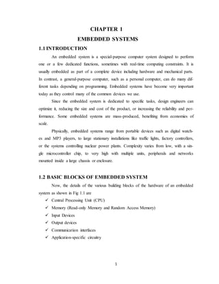
  • 1. 1 CHAPTER 1 EMBEDDED SYSTEMS 1.1 INTRODUCTION An embedded system is a special-purpose computer system designed to perform one or a few dedicated functions, sometimes with real-time computing constraints. It is usually embedded as part of a complete device including hardware and mechanical parts. In contrast, a general-purpose computer, such as a personal computer, can do many dif- ferent tasks depending on programming. Embedded systems have become very important today as they control many of the common devices we use. Since the embedded system is dedicated to specific tasks, design engineers can optimize it, reducing the size and cost of the product, or increasing the reliability and per- formance. Some embedded systems are mass-produced, benefiting from economies of scale. Physically, embedded systems range from portable devices such as digital watch- es and MP3 players, to large stationary installations like traffic lights, factory controllers, or the systems controlling nuclear power plants. Complexity varies from low, with a sin- gle microcontroller chip, to very high with multiple units, peripherals and networks mounted inside a large chassis or enclosure. 1.2 BASIC BLOCKS OF EMBEDDED SYSTEM Now, the details of the various building blocks of the hardware of an embedded system as shown in Fig 1.1 are  Central Processing Unit (CPU)  Memory (Read-only Memory and Random Access Memory)  Input Devices  Output devices  Communication interfaces  Application-specific circuitry
  • 2. 2 1.2.1 CENTRAL PROCESSING UNIT (CPU) The Central Processing Unit (processor, in short) can be any of the following: mi- crocontroller, microprocessor or Digital Signal Processor (DSP). A micro-controller is a low-cost processor. Its main attraction is that on the chip itself, there will be many other components such as memory, serial communication interface, analog-to digital converter etc. So, for small applications, a micro-controller is the best choice as the number of ex- ternal components required will be very less. On the other hand, microprocessors are more powerful, but you need to use many external components with them. DSP is used mainly for applications in which signal processing is involved such as audio and video processing. Fig 1.1: Block Diagram of Embedded System 1.2.2 MEMORY The memory is categorized as Random Access Memory (RAM) and Read Only Memory (ROM). The contents of the RAM will be erased if power is switched off to the chip, whereas ROM retains the contents even if the power is switched off. So, the firm- ware is stored in the ROM. When power is switched on, the processor reads the ROM; the program is executed.
  • 3. 3 1.2.3 INPUT DEVICES Unlike the desktops, the input devices to an embedded system have very limited capability. There will be no keyboard or a mouse, and hence interacting with the embed- ded system is not an easy task. Many embedded systems will have a small keypad-you press one key to give a specific command. A keypad may be used to input only the digits. Many embedded systems used in process control do not have any input device for user interaction; they take inputs from sensors or transducers and produce electrical signals that are in turn fed to other systems. 1.2.4 OUTPUT DEVICES The output devices of the embedded systems also have very limited capability. Some embedded systems will have a few Light Emitting Diodes (LEDs) to indicate the health status of the system modules, or for visual indication of alarms. A small Liquid Crystal Display (LCD) may also be used to display some important parameters. 1.2.5 COMMUNICATION INTERFACES The embedded systems may need to, interact with other embedded systems at they may have to transmit data to a desktop. To facilitate this, the embedded systems are provided with one or a few communication interfaces such as RS232, RS422, RS485, Universal Serial Bus (USB), and IEEE 1394, Ethernet etc. 1.2.6 APPLICATION-SPECIFIC CIRCUITRY Sensors, transducers, special processing and control circuitry may be required for an embedded system, depending on its application. This circuitry interacts with the pro- cessor to carry out the necessary work. The entire hardware has to be given power supply either through the 230 volts main supply or through a battery. The hardware has to design in such a way that the power consumption is minimized. Security is the condition of being protected against danger or loss. In the general sense, security is a concept similar to safety. The nuance between the two is an added emphasis on being protected from dangers that originate from outside. Individuals or ac- tions that encroach upon the condition of protection are responsible for the breach of se- curity. The word "security" in general usage is synonymous with "safety," but as a tech-
  • 4. 4 nical term "security" means that something not only is secure but that it has been secured. One of the best options for providing good security is by using a technology named EM- BEDDED SYSTEMS. 1.3 MICROCONTROLLER In the Literature discussing microprocessors, we often see the term Embedded System. Microprocessors and Microcontrollers are widely used in embedded system products. An embedded system product uses a microprocessor (or Microcontroller) to do one task only. A printer is an example of embedded system since the processor inside it performs one task only, namely getting the data and printing it. Contrast this with a Pen- tium based PC can be used for any number of applications such as word processor, print- server, bank teller terminal, Video game, network server, or Internet terminal. Software for a variety of applications can be loaded and run. Of course the reason a pc can perform myriad tasks is that it has RAM memory and an operating system that loads the applica- tion software into RAM memory and lets the CPU run it. In an Embedded system, there is only one application software that is typically burned into ROM. An x86 PC contains or is connected to various embedded products such as keyboard, printer, modem, disk controller, sound card, CD-ROM drives, mouse, and so on. Each one of these peripherals has a Microcontroller inside it that performs on- ly one task. For example, inside every mouse there is a Microcontroller to perform the task of finding the mouse position and sending it to the PC. 1.4 APPLICATION AREAS Nearly 99 per cent of the processors manufactured end up in embedded systems. The embedded system market is one of the highest growth areas as these systems are used in very market segment- consumer electronics, office automation, industrial automa- tion, biomedical engineering, wireless communication, data communication, telecommu- nications, transportation, military and so on. Consumer appliances: At home we use a number of embedded systems which include digital camera, digital diary, DVD player, video recorders etc. Office automation: The office automation products using embedded systems are copy- ing machine, fax machine, key telephone, modem, printer, scanner etc
  • 5. 5 Industrial automation: Today a lot of industries use embedded systems for process con- trol. In hazardous industrial environment, where human presence has to be avoided, ro- bots are used, which are programmed to do specific jobs. Medical electronics: Almost every medical equipment in the hospital is an embedded system. These equipments include diagnostic aids such as ECG, EEG, blood pressure measuring devices, radiation, colonoscopy, endoscopy etc. Computer networking: Computer networking products such as bridges, routers, Inte- grated Services Digital Networks (ISDN), Asynchronous Transfer Mode (ATM), X.25 and frame relay switches are embedded systems which implement the necessary data communication protocols Telecommunications: In the field of telecommunications, the embedded systems can be categorized as subscriber terminals and network equipment. The subscriber terminals such as key telephones, ISDN phones, terminal adapters, web cameras are embedded sys- tems. The network equipment includes multiplexers, multiple access systems, Packet As- semblers Dissemblers (PADs), sate11ite modems etc. Security: Security of persons and information has always been a major issue. We need to protect our homes and offices; and also the information we transmit and store. Devel- oping embedded systems for devices at homes, offices, airports etc. for authentication and verification are embedded systems security applications is one of the most lucrative businesses nowadays.
  • 6. 6 CHAPTER 2 GESTURE CONTROL ROBOT USING ACCELEROMETER 2.1 BLOCK DIAGRAM TRANSMITTER It consists of three modules in transmission section. They are as follows:  ADC Converter(LM324)  Encoder(HT12E)  Accelerometer(ADXL335)  RF Transmitter Fig 2.1: Block diagram of transmitter 2.1.1 POWER SUPPLY The input to the circuit is applied from the regulated power supply. The a.c. input i.e., 230V from the mains supply is step down by the transformer to 12V and is fed to a rectifier. The output obtained from the rectifier is a pulsating d.c voltage. So in order to get a pure d.c voltage, the output voltage from the rectifier is fed to a filter to remove any
  • 7. 7 a.c components present even after rectification. Now, this voltage is given to a voltage regulator to obtain a pure constant dc voltage. DC MOTORS Digital systems and microcontroller pins lack sufficient current to drive the cir- cuits like relays, buzzer circuits, motors etc. While these circuits require around 10milli amps to be operated, the microcontroller’s pin can provide a maximum of 1-2milli amps current. For this reason, a driver such as a power transistor is placed in between the mi- crocontroller and the motor.  VOLTAGE REGULATOR Voltage regulator ICs is available with fixed (typically 5, 12 and 15V) or variable output voltages. The maximum current they can pass also rates them. Negative voltage regulators are available, mainly for use in dual supplies. Most regulators include some automatic protection from excessive current ('overload protection') and overheating ('thermal protection'). Many of the fixed voltage regulator ICs has 3 leads and look like power transistors, such as the 7805 +5V 1A regulator shown on the right. The LM7805 is simple to use. You simply connect the positive lead of your unregulated DC power sup- ply (anything from 9VDC to 24VDC) to the Input pin, connect the negative lead to the Common pin and then when you turn on the power, you get a 5 volt supply from the out- put pin. Voltage regulator
  • 8. 8 2.1.2 ACCELEROMETER An accelerometer is an instrument for measuring acceleration, detecting and measuring vibrations, or for measuring acceleration due to gravity (inclination). Accel- erometers can be used to measure vibration on vehicles, machines, buildings, process control systems and safety installations. They can also be used to measure seismic activi- ty, inclination, machine vibration, dynamic distance and speed with or without the influ- ence of gravity. 2.1.3 ANALOG TO DIGITAL CONVERTER USING LM234 LM324 is used for Analog to Digital Conversion. It has four embedded op amps, which requires Vcc (5V) and ground only. Analog signal is fed to the parallel combina- tions of comparators, which produces an encoded signal corresponding to input analog signal. The encoded signal is then applied to Digital Code Converter (a combinational circuit), that will produce binary output. If the analog input exceeds the reference voltage to any comparator that comparator turns ON. 2.1.4 HT12E Encoders are software programs that are used for compressing information. Often, the function of an encoder will also allow for the conversion of data from one format to another. The HT12E is a 4bit encoder which encodes the input data applied on it. It con- verts the parallel inputs into serial output. It encodes the 12 bit parallel data into serial for transmission through an RF transmitter. These 12 bits are divided into 8 address bits and 4 data bits. HT12E has a transmission enable pin which is active low. When a trigger signal is received on TE pin, the programmed addresses/data are transmitted together with the header bits via an RF or an infrared transmission medium.
  • 9. 9 2.1.5 RF TRANSMITTER (TX) Transmitter is an electronic device which converts measurements from a sensor into a signal, and sends it, via wires or wireless, to be received by control device located a distance away .The transmitter (Tx) operates at a frequency of 434 MHz which re- ceives serial data and transmits it wirelessly through RF through its antenna. This trans- mission occurs at the rate of 1Kbps - 10Kbps. 2.2 BLOCK DIAGRAM OF RECEIVER It consists of three modules in this section. They are as follows  Microcontroller(AT89S52)  Decoder(HT12D)  Actuator(L293D)  RF Receiver Fig 2.3 Block Diagram of Receiver
  • 10. 10 2.2.1 RF RECEIVER RF receivers are the easiest way possible to add wireless control. It receives the data which is transferred by the gesture device whose working is similar to the transmitter module. The data pin is connected to HT12D decoder. 2.2.2 HT12D The HT12D converts the serial data into parallel data which is received by the RF receiver module. The input data is decoded when no error or unmatched codes are found. A valid transmission is indicated by a high signal at Voltage Terminal pin. 2.2.3 MICROCONTROLLER (AT89S52) The AT89S8252 is a low power, high performance CMOS 8-bit microcontrol- ler with 8K bytes of in system programmable Flash memory. It is associated of circuitry like Crystal with capacitors, Reset circuitry, Pull up resistors (if needed) and so on. The Microcontroller forms the heart of the project because it controls the devices being inter- faced and communicates with the devices according to the program being written. 2.2.4 ACTUATORS (L293D) The Actuators are those devices which gives the movement or to do a task like motors. In the real world there are various types of motors available which works on dif- ferent voltages so we need motor driver for running them through the controller. To get interfaced between motor and microcontroller we use L293D motor driver. 2.3 DESCRIPTION A Gesture Controlled robot is a kind of robot which can be controlled by your hand gestures not by old buttons. You just need to wear a small transmitting device in your hand which included an acceleration meter. This will transmit an appropriate com- mand to the robot so that it can do whatever we want. The transmitting device included a ADC for analog to digital conversion and an encoder IC(HT12E) which is use to encode the four bit data and then it will transmit by an RF Transmitter module.
  • 11. 11 At the receiving end an RF Receiver module receives the encoded data and decodes it by and decoder IC (HT12D). This data is then processed by a microcontroller and finally our motor driver to control the motors. As user makes movements of his hand in front of it, it senses and according to that it sends the signal for decision. Output from accelerometer is gathered for process by microcontroller. As per sensor output, the controller is made to work according to the program written inside it and it sends the respective signal to third part which is motors. This is the last part which drives the wheel of our robot. It uses two dc motors to make movement. To drive them one motor driver is IC used which provides sufficient current to motors. All this material is mounted on metal chesi. As we move our hand to right robot will move to right side. Similar to this it will copy all our movements. 2.4 WORKING PRINCIPLE Our gesture controlled robot works on the principle of accelerometer which rec- ords hand movements and send that data to the comparator which assigns proper voltage level to the recorded movements. That information is then transferred to an encoder which makes it ready for RF transmission. On the receiving end, the information is re- ceived wirelessly via RF Decoded information. These decisions are passed to the motor driver that is which triggers the motors in different configurations to make the robot move in specific direction.
  • 12. 12 CHAPTER 3 8051 MICROCONTROLLER 3.1 INTRODUCTION Microprocessors and microcontrollers are widely used in embedded systems products. A microcontroller has a CPU in addition to a fixed amount of RAM, ROM, I/O ports and a timer embedded all on a single chip. The fixed amount of on-chip ROM, RAM and number of I/O ports in microcontrollers makes them ideal for many applica- tions in which cost and space are critical. Fig: Microcontroller(AT89S52) The Intel 8051 is Harvard architecture, single chip microcontroller (µC) which was developed by Intel in 1980 for use in embedded systems 8051 is an 8-bit processor, meaning that the CPU can work on only 8 bits of data at a time. Data larger than 8 bits has to be broken into 8-bit pieces to be processed by the CPU. 8051 is available in different memory types such as UV-EPROM, Flash and NV- RAM. The microcontroller used in this project is AT89C51. Atmel Corporation intro- duced this 89C51 microcontroller. This microcontroller belongs to 8051 family. This mi-
  • 13. 13 crocontroller had 128 bytes of RAM, 4K bytes of on-chip ROM, two timers, one serial port and four ports (each 8-bits wide) all on a single chip. AT89C51 is Flash type 8051. The present project is implemented on Keil Uvision. In order to program the de- vice, Proload tool has been used to burn the program onto the microcontroller. The features, pin description of the microcontroller and the software tools used are discussed in the following sections. 3.2 FEATURES OF AT89C51  4K Bytes of Re-programmable Flash Memory.  RAM is 128 bytes.  2.7V to 6V Operating Range.  Fully Static Operation: 0 Hz to 24 MHz.  Two-level Program Memory Lock.  128 x 8-bit Internal RAM.  32 Programmable I/O Lines.  Two 16-bit Timer/Counters.  Six Interrupt Sources.  Programmable Serial UART Channel.  Low-power Idle and Power-down Modes. 3.3 DESCRIPTION The AT89C51 is a low-voltage, high-performance CMOS 8-bit microcomputer with 4K bytes of Flash programmable memory. The device is manufactured using Atmel’s high-
  • 14. 14 density nonvolatile memory technology and is compatible with the industry-standard MCS-51 instruction set. By combining a versatile 8-bit CPU with Flash on a monolithic chip, the Atmel AT89C51 is a powerful microcomputer, which provides a highly flexible and cost-effective solution to many embedded control applications. In addition, the AT89C51 is designed with static logic for operation down to zero fre- quency and supports two software selectable power saving modes. The Idle Mode stops the CPU while allowing the RAM, timer/counters, serial port and interrupt system to con- tinue functioning. The power-down mode saves the RAM contents but freezes the oscilla- tor disabling all other chip functions until the next hardware reset 3.3.2 BLOCK DIAGRAM Fig 3.2: Block Diagram of Microcontroller
  • 15. 15 3.3.1 PIN DIAGRAM Fig 3.1 Pin Diagram of Microcontroller 3.3.3 PIN DESCRIPTION Vcc Pin 40 provides supply voltage to the chip. The voltage source is +5V. GND Pin 20 is the ground. XTAL1 and XTAL2 XTAL1 and XTAL2 are the input and output, respectively, of an inverting amplifier that can be configured for use as an on-chip oscillator, as shown in Figure 11. Either a quartz crystal or ceramic resonator may be used. To drive the device from an external clock source, XTAL2 should be left unconnected while XTAL1 is driven, as shown in the be-
  • 16. 16 low figure. There are no requirements on the duty cycle of the external clock signal, since the input to the internal clocking circuitry is through a divide-by-two flip-flop, but mini- mum and maximum voltage high and low time specifications must be observed. Fig 3.3: Oscillator Connections C1, C2 = 30 pF ± 10 pF for Crystals = 40 pF ± 10 pF for Ceramic Resonators Fig 3.4: External Clock Drive Configuration
  • 17. 17 RESET Pin9 is the reset pin. It is an input and is active high. Upon applying a high pulse to this pin, the microcontroller will reset and terminate all the activities. This is often referred to as a power-on reset. EA (External access) Pin 31 is EA. It is an active low signal. It is an input pin and must be connected to either Vcc or GND but it cannot be left unconnected. The 8051 family members all come with on-chip ROM to store programs. In such cases, the EA pin is connected to Vcc. If the code is stored on an external ROM, the EA pin must be connected to GND to indicate that the code is stored externally. PSEN (Program store enable) This is an output pin. ALE (Address latch enable) This is an output pin and is active high. Ports 0, 1, 2 and 3 The four ports P0, P1, P2 and P3 each use 8 pins, making them 8-bit ports. All the ports upon RESET are configured as input, since P0-P3 have value FFH on them. Port 0(P0) Port 0 is also designated as AD0-AD7, allowing it to be used for both address and data. ALE indicates if P0 has address or data. When ALE=0, it provides data D0-D7, but when ALE=1, it has address A0-A7. Therefore, ALE is used for demultiplexing address and data with the help of an internal latch.
  • 18. 18 When there is no external memory connection, the pins of P0 must be connected to a 10K-ohm pull-up resistor. This is due to the fact that P0 is an open drain. With external pull-up resistors connected to P0, it can be used as a simple I/O, just like P1 and P2. But the ports P1, P2 and P3 do not need any pull-up resistors since they already have pull-up resistors internally. Upon reset, ports P1, P2 and P3 are configured as input ports. Port 1 and Port 2 With no external memory connection, both P1 and P2 are used as simple I/O. With ex- ternal memory connections, port 2 must be used along with P0 to provide the 16-bit ad- dress for the external memory. Port 2 is designated as A8-A15 indicating its dual func- tion. While P0 provides the lower 8 bits via A0-A7, it is the job of P2 to provide bits A8- A15 of the address. Port 3 Port 3 occupies a total of 8 pins, pins 10 through 17. It can be used as input or output. P3 does not need any pull-up resistors, the same as port 1 and port 2. Port 3 has an additional function of providing some extremely important signals such as interrupts. Table 3.1: Port 3 Alternate Functions 3.4 PROGRAMMING THE FLASH
  • 19. 19 The AT89C51 is normally shipped with the on-chip Flash memory array in the erased state (that is, contents = FFH) and ready to be programmed. The programming interface accepts either a high-voltage (12-volt) or a low-voltage (VCC) program enable signal. The low-voltage programming mode provides a convenient way to program the AT89C51 inside the user’s system, while the high-voltage programming mode is compat- ible with conventional third party Flash or EPROM programmers. The AT89C51 is shipped with either the high-voltage or low-voltage programming mode enabled. The re- spective top-side marking and device signature codes are listed in the following table. Table 3.2: Programming Flash The AT89C51 code memory array is programmed byte-byte in either programming mode. 3.4.1 PROGRAMMING ALGORITHM Before programming the AT89C51, the address, data and control signals should be set up according to the Flash programming mode table. To program the AT89C51, the follow- ing steps should be considered: 1. Input the desired memory location on the address lines. 2. Input the appropriate data byte on the data lines. 3. Activate the correct combination of control signals.
  • 20. 20 4. Raise EA/VPP to 12V for the high-voltage programming mode. 5. Pulse ALE/PROG once to program a byte in the Flash array or the lock bits. The byte- write cycle is self-timed and typically takes no more than 1.5 ms. Repeat steps 1 through 5, changing the address and data for the entire array or until the end of the object file is reached. 3.4.2 DATA POLLING The AT89C51 features Data Polling to indicate the end of a write cycle. During a write cycle, an attempted read of the last byte written will result in the complement of the writ- ten datum on PO.7. Once the write cycle has been completed, true data are valid on all outputs, and the next cycle may begin. Data Polling may begin any time after a write cy- cle has been initiated. Ready/Busy The progress of byte programming can also be monitored by the RDY/BSY output signal. P3.4 is pulled low after ALE goes high during programming to indicate BUSY. P3.4 is pulled high again when programming is done to indicate READY. 3.4.3 Chip erase The entire Flash array is erased electrically by using the proper combination of control signals and by holding ALE/PROG low for 10 ms. The code array is written with all “1”s. The chip erase operation must be executed before the code memory can be re- programmed.
  • 21. 21 Reading the Signature Bytes: The signature bytes are read by the same procedure as a normal verification of locations 030H, 031H, and 032H, except that P3.6 and P3.7 must be pulled to a logic low. The val- ues returned are as follows. (030H) = 1EH indicates manufactured by Atmel (031H) = 51H indicates 89C51 (032H) = FFH indicates 12V programming (032H) = 05H indicates 5V programming 3.4.4 PROGRAMMING INTERFACE Every code byte in the Flash array can be written and the entire array can be erased by using the appropriate combination of control signals. The write operation cycle is self timed and once initiated, will automatically time itself to completion. All major pro- gramming vendors offer worldwide support for the Atmel microcontroller series. Table 3.3: Flash programming mode
  • 22. 22 Fig 3.5: Programming the Flash Fig: 3.6: Verifying the Flas
  • 23. 23 CHAPTER 4 RF WIRELESS COMMUNICATIONS 4.1 INTRODUCTION Radio frequency (RF) is a frequency or rate of oscillation within the range of about 3 Hz to 300 GHz. This range corresponds to frequency of alternating current elec- trical signals used to produce and detect radio waves. Since most of this range is beyond the vibration rate that most mechanical systems can respond to, RF usually refers to oscil- lations in electrical circuits or electromagnetic radiation. What is RF? RF itself has become synonymous with wireless and high-frequency signals, describing anything from AM radio between 535 kHz and 1605 kHz to computer local area net- works (LANs) at 2.4 GHz. However, RF has traditionally defined frequencies from a few kHz to roughly 1 GHz. If one considers microwave frequencies as RF, this range extends to 300 GHz. The following two tables outline the various nomenclatures for the frequen- cy bands. The third table outlines some of the applications at each of the various frequen- cy bands. 4.2 PROPERTIES OF RF Electrical currents that oscillate at RF have special properties not shared by direct current signals. One such property is the ease with which it can ionize air to create a conductive path through air. This property is exploited by 'high frequency' units used in electric arc welding. Another special property is an electromagnetic force that drives the RF current to the surface of conductors, known as the skin effect. Another property is the ability to appear to flow through paths that contain insulating material, like the dielectric insulator of a capacitor. The degree of effect of these properties depends on the frequency of the signals.
  • 24. 24 4.3 BRIEF DESCRIPTION OF RF Radio frequency (abbreviated RF) is a term that refers to alternating current (AC) having characteristics such that, if the current is input to an antenna, an electromagnetic (EM) field is generated suitable for wireless broadcasting and/or communications. These fre- quencies cover a significant portion of the electromagnetic radiation spectrum, extending from nine kilohertz (9 kHz),the lowest allocated wireless communications frequency (it's within the range of human hearing), to thousands of gigahertz(GHz). When an RF current is supplied to an antenna, it gives rise to an electromagnetic field that propagates through space. This field is sometimes called an RF field; in less tech- nical jargon it is a "radio wave." Any RF field has a wavelength that is inversely propor- tional to the frequency s = 300/f The RF spectrum is divided into several ranges, or bands. With the exception of the low- est-frequency segment, each band represents an increase of frequency corresponding to an order of magnitude (power of 10). The table depicts the eight bands in the RF spec- trum, showing frequency and bandwidth ranges. The SHF and EHF bands are often re- ferred to as the microwave spectrum. 4.4 RF ADVANTAGES  No line of sight is needed.  Not blocked by common materials: It can penetrate most solids and pass through walls.  Longer range.  It is not sensitive to the light.  It is not much sensitive to the environmental changes and weather conditions.
  • 25. 25 4.5 WHAT ARE THE MAIN REQUIREMENTS FOR THE COMMU- NICATION USING RF?  RF Transmitter  RF Receiver  Encoder and Decoder 4.6 RF TRANSMITTER STT-433MHz Fig 4.1: RF Transmitter 4.6.1 FACTORS INFLUENCED TO CHOOSE STT-433MHz ABOUT THE TRANSMITTER  The STT-433 is ideal for remote control applications where low cost and longer range is required.  The transmitter operates from a1.5-12V supply, making it ideal for battery- powered applications.  The transmitter employs a SAW-stabilized oscillator, ensuring accurate frequency control for best range performance.  The manufacturing-friendly SIP style package and low-cost make the STT-433 suitable for high volume applications.
  • 26. 26 4.6.2 FEATURES  433.92 MHz Frequency  Low Cost  1.5-12V operation  Small size 4.6.3 PIN DESCRIPTION Fig4.2: Pin Diagram of RF Transmitter GND: Transmitter ground. Connect to ground plane DATA: Digital data input. This input is CMOS compatible and should be driven with CMOS level inputs. VCC: Operating voltage for the transmitter. VCC should be bypassed with a .01uF ceramic capacitor and filtered with a 4.7uF tantalum capacitor. Noise on the power sup- ply will degrade transmitter noise performance. ANT: 50 ohm antenna output. The antenna port impedance affects output power and harmonic emissions. Antenna can be single core wire of approximately 17cm length or PCB trace antenna. 4.5.5 APPLICATION The typical connection shown in the above figure cannot work exactly at all times be- cause there will be no proper synchronization between the transmitter and the microcon-
  • 27. 27 troller unit. i.e., whatever the microcontroller sends the data to the transmitter, the trans- mitter is not able to accept this data as this will be not in the radio frequency range. Fig 4.3 Application Circuit Thus, we need an intermediate device which can accept the input from the microcontrol- ler, process it in the range of radio frequency range and : send it to the transmitter. 4.7 RF RECEIVER STR-433 MHz The data is received by the RF receiver from the antenna pin and this data is available on the data pins. Fig 4.4: RF Receiver The data is received by the RF receiver from the antenna pin and this data is available on the data pins. Two Data pins are provided in the receiver module. Thus, this data can be used for further applications.
  • 28. 28 4.7.1 PIN DIAGRAM Fig 4.5: Pin Diagram of RF Receiver 4.7.2 PIN DESCRIPTION ANT: Antenna input. GND: Receiver Ground. Connect to ground plane. VCC (5V): VCC pins are electrically connected and provide operating voltage for the receiver. VCC can be applied to either or both. VCC should be bypassed with a .1μF ce- ramic capacitor. Noise on the power supply will degrade receiver sensitivity. DATA: Digital data output. This output is capable of driving one TTL or CMOS load. It is a CMOS compatible output. APPLICATIONS: Similarly, as the transmitter requires an encoder, the receiver module requires a decoder. The decoder used is HT12D from HOLTEK SEMICONDUCTOR INC.
  • 29. 29 CHAPTER 5 HARDWARE DESCRIPTION 5.1 HT12E-212 SERIES OF ENCODERS Fig 5.1: Pin Diagram 5.1.1 FEATURES  Operating voltage  2.4V~5V for the HT12A  2.4V~12V for the HT12E  Low power and high noise immunity CMOS technology  Low standby current: 0.1_A (typ.) at VDD=5V  Minimum transmission word  Four words for the HT12E  Built-in oscillator needs only 5% resistor  Data code has positive polarity  Minimal external components  HT12E: 18-pin DIP/20-pin SOP pack
  • 30. 30 5.1.2 GENERAL DESCRIPTION The 212 encoders are a series of CMOS LSIs for remote control system applica- tions. They are capable of encoding information which consists of N address bits and 12_N data bits. Each address/data input can be set to one of the two logic states. The pro- grammed addresses/data are transmitted together with the header bits via an RF or an in- frared transmission medium upon receipt of a trigger signal. The capability to select a TE trigger on the HT12E further enhances the application flexibility of the 212 series of en- coders. 5.1.3 BLOCK DIAGRAM OF ENCODER Fig 5.2: Block Diagram Table 5.2: Pin description of HT12E 5.1.4 FUNCTIONAL DESCRIPTION Operation The 212 series of encoders begin a 4-word transmission cycle upon receipt of a transmission enable (TE for the HT12E active low). This cycle will repeat itself as long
  • 31. 31 as the transmission enable (TE or D8~D11) is held low. Once the transmission enable returns high, the encoder output completes its final cycle and then stops as shown below. Address/data waveform Each programmable address/data pin can be externally set to one of the following two logic states as shown below. Address/data programming (preset) The status of each address/data pin can be individually pre-set to logic _high_ or _low_. If a transmission- enable signal is applied, the encoder scans and transmits the sta- tus of the 12 bits of address/data serially in the order A0 to AD11 for the HT12E encoder. During information transmission these bits are transmitted with a preceding synchroniza- tion bit. If the trigger signal is not applied, the chip enters the standby mode and con- sumes a reduced current of less than 1_A for a supply voltage of 5V. Usual applications
  • 32. 32 preset the address pins with individual security codes using DIP switches or PCB wiring, while the data is selected by push buttons or electronic switches. 5.1.5 FLOW CHART Fig 5.3: Flow Chart of Encoder
  • 33. 33 5.1.6 APPLICATION CIRCUIT Fig 5.4: Application of Transmitter 5.2 HT12D-212 SERIES OF DECODERS 5.2.1 PIN DIAGRAM Fig 5.5: Pin Diagram 5.2.2 FEATURES  Operating voltage: 2.4V~12V
  • 34. 34  Low power and high noise immunity CMOS technology  Low standby current  Capable of decoding 12 bits of information  Binary address setting  Received codes are checked 3 times  Address/Data number combination  HT12D: 8 address bits and 4 data bits  Built-in oscillator needs only 5% resistor  Valid transmission indicator  Easy interface with an RF or an infrared transmission medium  Minimal external components  Pair with Holtek’s 212 series of encoders  18-pin DIP, 20-pin SOP package 5.2.3 GENERAL DESCRIPTION The 212 decoders are a series of CMOS LSIs for remote control system applica- tions. They are paired with Holtek’s 212 series of encoders. For proper operation, a pair of encoder/decoder with the same number of addresses and data format should be chosen. The decoders receive serial addresses and data from a programmed 212 series of encoders that are transmitted by a carrier using an RF or an IR transmission medium. They com- pare the serial input data three times continuously with their local addresses. If no error or unmatched codes are found, the input data codes are decoded and then transferred to the output pins. The VT pin also goes high to indicate a valid transmission. The 212 series of decoders are capable of decoding information that consists of N bits of address and 12_N bits of data. Of this series, the HT12D is arranged to provide 8 address bits and 4 data bits, and HT12F is used to decode 12 bits of address information.
  • 35. 35 5.2.4 BLOCKDIAGRAM OF DECODER Fig 5.6: Block Diagram 5.2.5 PIN DESCRIPTION Table 5.3: Pin description of HT12D
  • 36. 36 5.2.6 FUNCTIONAL DESCRIPTION Operation The 212 series of decoders provides various combinations of addresses and data pins in different packages so as to pair with the 212 series of encoders. The decoders re- ceive data that are transmitted by an encoder and interpret the first N bits of code period as addresses and the last 12_N bits as data, where N is the address code number. A signal on the DIN pin activates the oscillator which in turn decodes the incoming address and data. The decoders will then check the received address three times continuously. If the received address codes all match the contents of the decoder’s local address, the 12_N bits of data are decoded to activate the output pins and the VT pin is set high to indicate a valid transmission. This will last unless the address code is incorrect or no signal is re- ceived. The output of the VT pin is high only when the transmission is valid. Otherwise it is always low. 5.2.7 FLOW CHART Fig 5.7: Flow Chart of Decoder
  • 37. 37 5.3 ACTUATOR (L293D) 5.3.1 PIN DIAGRAM Fig 5.9: Pin Diagram 5.3.2 FEATURES  Wide Supply-Voltage Range: 4.5 V to 36 V  Separate Input-Logic Supply  Internal ESD Protection  Thermal Shutdown  High-Noise-Immunity Inputs  Functionally Similar to SGS L293 and SGS L293D  Output Current 1 A Per Channel (600 mA for L293D)  Peak Output Current 2 A Per Channel (1.2 A for L293D)  Output Clamp Diodes for Inductive Transient Suppression (L293D) 5.3.3 DESCRIPTION The L293 and L293D are quadruple high-current half-H drivers. The L293 is de- signed to provide bidirectional drive currents of up to 1 A at voltages from 4.5 V to 36 V. The L293D is designed to provide bidirectional drive currents of up to 600-mA at voltag- es from 4.5 V to 36 V. Both devices are designed to drive inductive loads such as relays, solenoids, dc and bipolar stepping motors, as well as other high-current/high-voltage loads in positive-supply applications.
  • 38. 38 All inputs are TTL compatible. Each output is a complete totem-pole drive circuit, with a Darlington transistor sink and a pseudo- Darlington source. Drivers are enabled in pairs, with drivers 1 and 2 enabled by 1,2EN and drivers 3 and 4 enabled by 3,4EN. When an enable input is high, the associated drivers are enabled and their outputs are active and in phase with their inputs. When the enable input is low, those drivers are disabled and their outputs are off and in the high-impedance state. With the proper data inputs, each pair of drivers forms a full-H (or bridge) reversible drive suitable for solenoid or motor applica- tions. On the L293, external high-speed output clamp diodes should be used for inductive transient suppression. A VCC1 terminal, separate from VCC2, is provided for the logic inputs to minimize de- vice power dissipation. The L293 and L293D are characterized for operation from 0 to 70 degree Celsius. 5.3.4 BLOCK DIAGRAM Fig 5.10: Block Diagram
  • 39. 39 CHAPTER 6 ACCELEROMETER ADXL335 6.1 INTRODUCTION An accelerometer is an electromechanical device that will measure acceleration forces. These forces may be static, like the constant force of gravity pulling at your feet, or they could be dynamic - caused by moving or vibrating the accelerometer. 6.1.1 USES OF ACCELEROMETER By measuring the amount of static acceleration due to gravity, you can find out the angle the device is tilted at with respect to the earth. By sensing the amount of dy- namic acceleration, you can analyze the way the device is moving. At first, measuring tilt and acceleration doesn't seem all that exciting. However, engineers have come up with many ways to make really useful products with them. An accelerometer can help your project understand its surroundings better. Is it driving uphill? Is it going to fall over when it takes another step? Is it flying horizontally or is it dive bombing your professor? A good programmer can write code to answer all of these questions using the data provided by an accelerometer. 6.1.2 WORKING OF AN ACCELEROMETER There are many different ways to make an accelerometer! Some accelerometers use the piezoelectric effect - they contain microscopic crystal structures that get stressed by accelerative forces, which cause a voltage to be generated. Another way to do it is by sensing changes in capacitance. If you have two microstructures next to each other, they have a certain capacitance between them. If an accelerative force moves one of the struc- tures, then the capacitance will change. Add some circuitry to convert from capacitance to voltage, and you will get an accelerometer. There are even more methods, including use of the piezoresistive effect, hot air bubbles, and light
  • 40. 40 6.1.3 TYPES OF ACCELEROMETER There are several different principles upon which an analog accelerometer can be built. Two very common types utilize capacitive sensing and the piezoelectric effect to sense the displacement of the proof mass proportional to the applied acceleration. 6.2 CAPACITIVE Accelerometers that implement capacitive sensing output a voltage dependent on the distance between two planar surfaces. One or both of these are charged with an elec- trical current. Changing the gap between the plates changes the electrical capacity of the system, which can be measured as a voltage output. This method of sensing is known for its high accuracy and stability. Capacitive accelerometers are also less prone to noise and variation with temperature, typically dissipates less power, and can have larger band- widths due to internal feedback circuitry. (Elwenspoek 1993) 6.3 PIEZOELECTRIC Piezoelectric sensing of acceleration is natural, as acceleration is directly propor- tional to force. When certain types of crystal are compressed, charges of opposite polarity accumulate on opposite sides of the crystal. This is known as the piezoelectric effect. In a piezoelectric accelerometer, charge accumulates on the crystal and is translated and am- plified into either an output current or voltage. Piezoelectric accelerometers only respond to AC phenomenon such as vibration or shock. They have a wide dynamic range, but can be expensive depending on their quality (Doscher 2005) Piezo-film based accelerometers are best used to measure AC phenomenon such as vibration or shock, rather than DC phenomenon such as the acceleration of gravity.
  • 41. 41 They are inexpensive, and respond to other phenomenon such as temperature, sound, and pressure (Doscher 2005) 6.4 OTHER There are many other types of accelerometer that are less important to musical applications, including:  Piezoresistive  Thermal  Null-balance  Servo force balance  Strain gauge  Resonance  Magnetic induction  Optical  Surface acoustic wave (SAW) 6.5 SPECIFICATIONS A typical accelerometer has the following basic specifications:  Analog/digital  Number of axes  Output range (maximum swing)  Sensitivity (voltage output per g)  Bandwidth  Amplitude stability The user selects the bandwidth of the accelerometer using the C X, CY, and CZ capacitors at the XOUT, YOUT, and ZOUT pins. Bandwidths can be selected to suit the
  • 42. 42 application, with a range of 0.5 Hz to 1600 Hz for the X and Y axes, and a range of 0.5 Hz to 54350 Hz for the Z axis. 6.6 GENERAL DESCRIPTION The ADXL335 is a small, thin, low power, complete 3-axis accelerometer with signal conditioned voltage outputs. The product measures acceleration with a mini- mum full-scale range of ±3 g. It can measure the static acceleration of gravity in tilt- sensing applications, as well as dynamic Acceleration resulting from motion, shock, or vibration. One of the most common inertial sensors is the accelerometer, a dynamic sensor capable of a vast range of sensing. Accelerometers are available that can measure accel- eration in one, two, or three orthogonal axes. They are typically used in one of three modes:  As an intertial measurement of velocity and position  As a sensor of inclination, tilt, or orientation in 2 or 3 dimensions, as referenced from the acceleration of gravity (1 g = 9.8m/s2);  As a vibration or impact (shock) sensor. There are considerable advantages to using an analog accelerometer as opposed to an inclinometer such as a liquid tilt sensor – inclinometers tend to output binary infor- mation (indicating a state of on or off), thus it is only possible to detect when the tilt has exceeded some thresholding angle. Most accelerometers are Micro-Electro-Mechanical Sensors (MEMS). The basic principle of operation behind the MEMS accelerometer is the displacement of a small proof mass etched into the silicon surface of the integrated circuit and suspended by small beams. Consistent with Newton's second law of motion (F = ma), as an acceleration is applied to the device, a force develops which displaces the mass. The support beams act
  • 43. 43 as a spring, and the fluid (usually air) trapped inside the IC acts as a damper, resulting in a second order lumped physical system. This is the source of the limited operational bandwidth and non-uniform frequency response of accelerometers. For more information, see reference to Elwenspoek, 1993.19 Fig 6.0: Block Diagram of ADXL335 An Accelerometer is a kind of sensor which gives an analog data while moving in X,Y,Z direction or may be X,Y direction only depends on the type of the sensor. Here is a small image of an Accelerometer shown. We can see in the image that there is some arrow showing if we tilt these sensors in that direction then the data at that corresponding pin will change in the analog form. A Microelectromechanical system (MEMS) is the technology of very small me- chanical devices driven by electricity; it merges at the nano-scale into nanoelectrome- chanical systems (NEMS) and nanotechnology.
  • 44. 44 Recent advances in microelectronic mechanical systems (MEMS) have made high-performance, high-accuracy, low-cost accelerometers available on a single mono- lithic IC. Accelerometers are used for acceleration and tilt measurements, vibration con- trol, and cutoff switches for specific vibration conditions. Fig 6.1: Accelerometer The accelerometer output is ac-coupled to the on-board amplifier so that slower variations due to tilt or any other signal of constant magnitude are rejected. To obtain the desired output, this on-board amplifier is used as a bandpass filter, as shown in the sche- matic. Then the signal is rectified and fed to a comparator, IC2. The output from the comparator generates a square pulse each time the magnitude of the jerk is more than a preset value. The comparator's output is used to trigger a one-shot, implemented using a 555 timer. The timer output, in turn, drives the alarm circuitry. Recent advances in microelectronic mechanical systems (MEMS) have made high-performance, high-accuracy, low-cost accelerometers available on a single mono- lithic IC. Accelerometers are used for acceleration and tilt measurements, vibration con- trol, and cutoff switches for specific vibration conditions.
  • 45. 45 6.7 PIN FUNCTIONAL DESCRIPTIONS Table 6.1: Pin Functional Description 6.8 FEATURES  3 axis sensing small, low profile package  4mm x 4mm x 1.45mm LFCSP low power:350uA(typical)  Single operation: 1.8v to 3.6v 10,000g shock survival  excellent temperature stability BW adjustment with a single capacitor per axis  RoHS/WEEE lead-free complement
  • 46. 46 CHAPTER 7 SOFTWARE DESCRIPTION 7.1 KEIL SOFTWARE In this module we will be using an Integrated Development Environment from Keil Electronic. This IDE is called u VISION (pronounced “Micro Vision”) and versions already exist for other popular microcontrollers including the 8051 and the Infineon C16X family. keil u vision successfully integrates project management, editor, compiler and debugger in one seamless front-end. Although we are concentrating on the LPC2000 family in this book, the Keil ARM tools can be used for any other ARM7 based micro- controller. Use of keil u vision to write a program for ARM processor. Keil compiler is software used where the machine language code is written and compiled. After compilation, the machine source code is converted into hex code which is to be dumped into the microcontroller for further processing. Keil compiler also sup- ports C language code. STEPS TO WRITE AN ASSEMBLY LANGUAGE PROGRAM IN KEIL AND HOW TO COMPILE IT 1. Install the Keil Software in the PC in any of the drives. 2. After installation, an icon will be created with the name “Keil uVision3”. Just drag this icon onto the desktop so that it becomes easy whenever you try to write programs in keil. 3. Double click on this icon to start the keil compiler. 4. A page opens with different options in it showing the project workspace at the leftmost corner side, output window in the bottom and an ash coloured space for the program to be written. 5. Now to start using the keil, click on the option “project”. 6. A small window opens showing the options like new project, import project, open project etc. Click on “New project”.
  • 47. 47 7. A small window with the title bar “Create new project” opens. The window asks the user to give the project name with which it should be created and the destina- tion location. The project can be created in any of the drives available. You can create a new folder and then a new file or can create directly a new file. 8. After the file is saved in the given destination location, a window opens where a list of vendors will be displayed and you have to select the device for the target you have created. 9. The most widely used vendor is Atmel. So click on Atmel and now the family of microcontrollers manufactured by Atmel opens. You can select any one of the microcontrollers according to the requirement. 10. When you click on any one of the microcontrollers, the features of that particular microcontroller will be displayed on the right side of the page. The most appro- priate microcontroller with which most of the projects can be implemented is the AT89C51. Click on this microcontroller and have a look at its features. Now click on “OK” to select this microcontroller. 11. A small window opens asking whether to copy the startup code into the file you have created just now. Just click on “No” to proceed further. 12. Now you can see the TARGET and SOURCE GROUP created in the project workspace. 13. Now click on “File” and in that “New”. A new page opens and you can start writ- ing program in it. 14. After the program is completed, save it with any name but with the .asm exten- sion. Save the program in the file you have created earlier. 15. You can notice that after you save the program, the predefined keywords will be highlighted in bold letters. 16. Now add this file to the target by giving a right click on the source group. A list of options open and in that select “Add files to the source group”. Check for this file where you have saved and add it. 17. Right click on the target and select the first option “Options for target”. A window opens with different options like device, target, output etc. First click on “target”.
  • 48. 48 18. Since the set frequency of the microcontroller is 11.0592 MHz to interface with the PC, just enter this frequency value in the Xtal (MHz) text area and put a tick on the Use on-chip ROM. This is because the program what we write here in the keil will later be dumped into the microcontroller and will be stored in the inbuilt ROM in the microcontroller. 19. Now click the option “Output” and give any name to the hex file to be created in the “Name of executable” text area and put a tick to the “Create HEX file” option present in the same window. The hex file can be created in any of the drives. You can change the folder by clicking on “Select folder for Objects”. 20. Now to check whether the program you have written is errorless or not, click on the icon exactly below the “Open file” icon which is nothing but Build Target icon. You can even use the shortcut key F7 to compile the program written. 21. To check for the output, there are several windows like serial window, memory window, project window etc. Depending on the program you have written, select the appropriate window to see the output by entering into debug mode. 22. The icon with the letter “d” indicates the debug mode. 23. Click on this icon and now click on the option “View” and select the appropriate window to check for the output. 24. After this is done, click the icon “debug” again to come out of the debug mode. 25. The hex file created as shown earlier will be dumped into the microcontroller. 7.2 FLASH MAGIC: NXP Semiconductors produce a range of Microcontrollers that feature both on- chip Flash memory and the ability to be reprogrammed using In-System Programming technology. Flash Magic is Windows software from the Embedded Systems Academy that allows easy access to all the ISP features provided by the devices.  STEP 1 – CONNECTION SETTINGS: Before the device can be used the settings required to make a connection must be specified. Select the desired COM port from the drop down list or type the desired COM
  • 49. 49 port directly into the box. If you enter the COM port yourself then you must enter it in one of the following formats: • COM n Any other format will generate an error. So if you want to use COM 5 (which is not present on the drop down list) you can directly type in either “COM 5” or “5”. Select the baud rate to connect at. Try a low speed first. The maximum speed that can be used depends on the crystal frequency on your hardware. You can try connecting at higher and higher speeds until connections fail. Then you have found the highest baud rate to connect at. Alternatively, some devices support high speed communications. Please refer to the High Speed Communications section for information. Select the device being used from the drop down list. Ensure you select the cor- rect one as different devices have different feature sets and different methods of setting up the serial communications. Select the interface being used, if any. An interface is a device that connects be- tween your PC and the target hardware. If you simply have a serial cable or USB to serial cable connecting your COM port to the target hardware, then choose "None (ISP)". Choosing the correct interface will automatically configure Flash Magic for that inter- face, along with enabling and disabling the relevant features. Enter the oscillator frequency used on the hardware. Do not round the frequency, instead enter it as precisely as possible. Some devices do not require the oscillator fre- quency to be entered, so this field will not be displayed. Once the options are set ensure the device is running the on-chip Boot loader if you are using a manual ISP entry method. Note that the connection settings affect all ISP features provided by Flash Magic.  STEP 2 – ERASING: This step is optional, however if you attempt to program the device without first erasing at least one Flash block, then Flash Magic will warn you and ask you if you are sure you want to program the device. Select each Flash block that you wish to erase by clicking on its name. If you wish to erase all the Flash then check that option. If you check to erase a Flash block and
  • 50. 50 all the Flash then the Flash block will not be individually erased. If you wish to erase on- ly the Flash blocks used by the hex file you are going to select, then check that option. For most devices erasing all the Flash also results in the Boot Vector and Status Byte being set to default values, which ensure that the Boot loader will be executed on reset, regardless of the state of the PSEN pin or other hardware requirements. Only when programming a Hex File has been completed will the Status Byte be set to 00H to allow the code to execute. This is a safeguard against accidentally attempting to execute when the Flash is erased. On some devices erasing all the Flash will also erase the security bits. This will be indicated by the text next to the Erase all Flash option. On some devices erasing all the Flash will also erase the speed setting of the device (the number of clocks per cycle) setting it back to the default. This will be indicated by the text next to the Erase all Flash option.  STEP 3 – SELECTING THE HEX FILE: This step is optional. If you do not wish to program a Hex File then do not select one. You can either enter a path name in the text box or click on the Browse button to select a Hex File by browsing to it. Also you can choose Open… from the File menu. Note that the Hex file is not loaded or cached in any way. This means that if the Hex File is modified, you do not have to reselect it in Flash Magic. Every time the Hex File is programmed it is first re-read from the location specified in the main window. The date the Hex file was last modified is shown in this section. This information is updated whenever the hex file is modified. The hex file does not need to be reselected. Clicking on more info or choosing Information… from the File menu will display additional information about the Hex file. The information includes the range of Flash memory used by the Hex file, the number of bytes of Flash memory used and the per- centage of the currently selected device that will be filled by programming the Hex file. If the device supports programming and execution from RAM, for example the ARM devices, then the hex file may contain records for the RAM. First the flash will be programmed followed by the RAM. Programs loaded into RAM via a hex file may be executed using such features as the Go option.
  • 51. 51  STEP 4 – OPTIONS: Flash Magic provides various options that may be used after the Hex File has been programmed. This section is optional, however Verify After Programming, Fill Un- used Flash and Gen Block Checksums may only be used if a Hex File is selected (and therefore being programmed), as they all need to know either the Hex File contents or memory locations used by the Hex File. Checking the Verify after Programming option will result in the data contained in the Hex File being read back from Flash and compared with the Hex File after program- ming. This helps to ensure that the Hex File was correctly programmed. If the device does not support verifying then this item will be disabled. Checking the Fill Unused Flash option will result in every memory location not used by the Hex File being programmed with the value that sets all the bits to a pro- grammed state. Once a location has been programmed with this feature it cannot be re- programmed with any other value, preventing someone from programming the device with a small program to read out the contents of Flash or altering the application’s opera- tion. Checking the Gen Block Checksums option will instruct Flash Magic to program the highest location in every Flash block used by the Hex File with a special “checksum adjuster value”. This value ensures that when a checksum is calculated for the whole Flash Block it will equal 55H, providing the contents of the Flash block have not be al- tered or corrupted.  STEP 5 – PERFORMING THE OPERATIONS: Step 5 contains a Start button. Clicking the Start button will result in all the se- lected operations in the main window taking place. They will be in order:  Erasing Flash  Programming the Hex File  Verifying the Hex File  Filling Unused Flash
  • 52. 52  Generating Checksums  Programming the clocks bit  Programming the Security Bits  Executing the firmware Once started progress information and a progress bar will be displayed at the bot- tom of the main window. In addition the Start button will change to a cancel button. Click on the cancel button to cancel the operation. Note that if you cancel during erasing all the Flash, it may take a few seconds be- fore the operation is cancelled. Once the operations have finished the progress information will briefly show the message “Finished…”. The Programmed Count shown next to the progress bar will in- crement. This shows the total number of times the hex file has been programmed. Modi- fying the hex file or selecting another hex file will reset the count. Alternatively, right- clicking over the count provides a menu with the option to immediately reset the count. Fig:7.2 Select Atmel
  • 53. 53 CHAPTER 8 RESULT ANALYSIS In future several wheelchairs (up to 128) can be operated using a single remote with accelerometer and PIC as master and various wheelchairs developed using micro- controllers as slave. This system can be extended by including GSM which sends an SMS during emergency by assigning particular gesture command. By including GPS, position of the wheelchair can also be known. Wheel chair can be fitted with direct mind reader. For ex- ample, if a person is parlyzand cannot move his body parts, in that case it can be used. Fig. 8.1 Move Forward Fig. 8.2 Move Backward Fig 8.3 Move Right Fig 8.4 Move Left
  • 54. 54 FLOW CHART start Transmit data through accel- erometer Receive data by WS-RX-02 receiver If data is 0101 If data is0010 If data is 1000 If data is 1010 Move robot forward Move robot backward Move robot left Move robot right stop
  • 55. 55 FIG 8.6: Gesture control robot
  • 56. 56 CONCLUSION The project “GESTURE CONTROL ROBOT USING ACCELEROMETER BASED” has been successfully designed and tested. Presence of every module has been reasoned out and placed carefully thus con- tributing to the best working of the unit. In our project we have added special features by which our robot can overcome so many problems in industry. If it is further developed then it can be used for military application
  • 57. 57 ADVANTAGES ADVANTAGES  We generally find people working in chemical industries under different hazard- ous condition. These people suffer with many dangerous diseases like skin cancer, lungs problem and many more.  So we finally thought of designing a robot that can copy that instant action of hu- man being under various conditions and situations. So in that place of industry it can be used.  Gestures can be used to control interactions for entertainment purposes such as gaming to make the game player’s experience more interactive or immersive  It is also used in mines FUTURE SCOPE  In future we can design a wireless robot which can sense hand gesture by us- ing wireless technologies.  It can be used in military applications as a robotic vehicle which can be han- dled by a soldier to avoid casualties.  Our system has shown the possibility that interaction with machines through gestures is a feasible task and the set of detected gestures could be enhanced to more commands by implementing a more complex model of a advanced vehicle for not only in limited space while also in broader area as in the roads too.  In the future, service robot executing many different tasks from private movement to a full- fledged advanced automotive that can make disabled to able in all sense
  • 58. 58 BIBLIOGRAPHY The 8051 Micro controller and Embedded Systems Muhammad Ali Mazidi Janice Gillispie Mazidi The 8051 Micro controller Architecture, Programming & Applications Kenneth J.Ayala Fundamentals Of Micro processors and Micro computers B.Ram Micro processor Architecture, Programming & Applications Ramesh S. Gaonkar Electronic Components D.V. Prasad Wireless Communications Theodore S. Rappaport
  • 59. 59 REFERENCES  http:// www.atmel.com  http:// www.beyondlogic.org  http://www.wikipedia.org  http://www.howstuffworks.com  http://www.alldatasheets.com