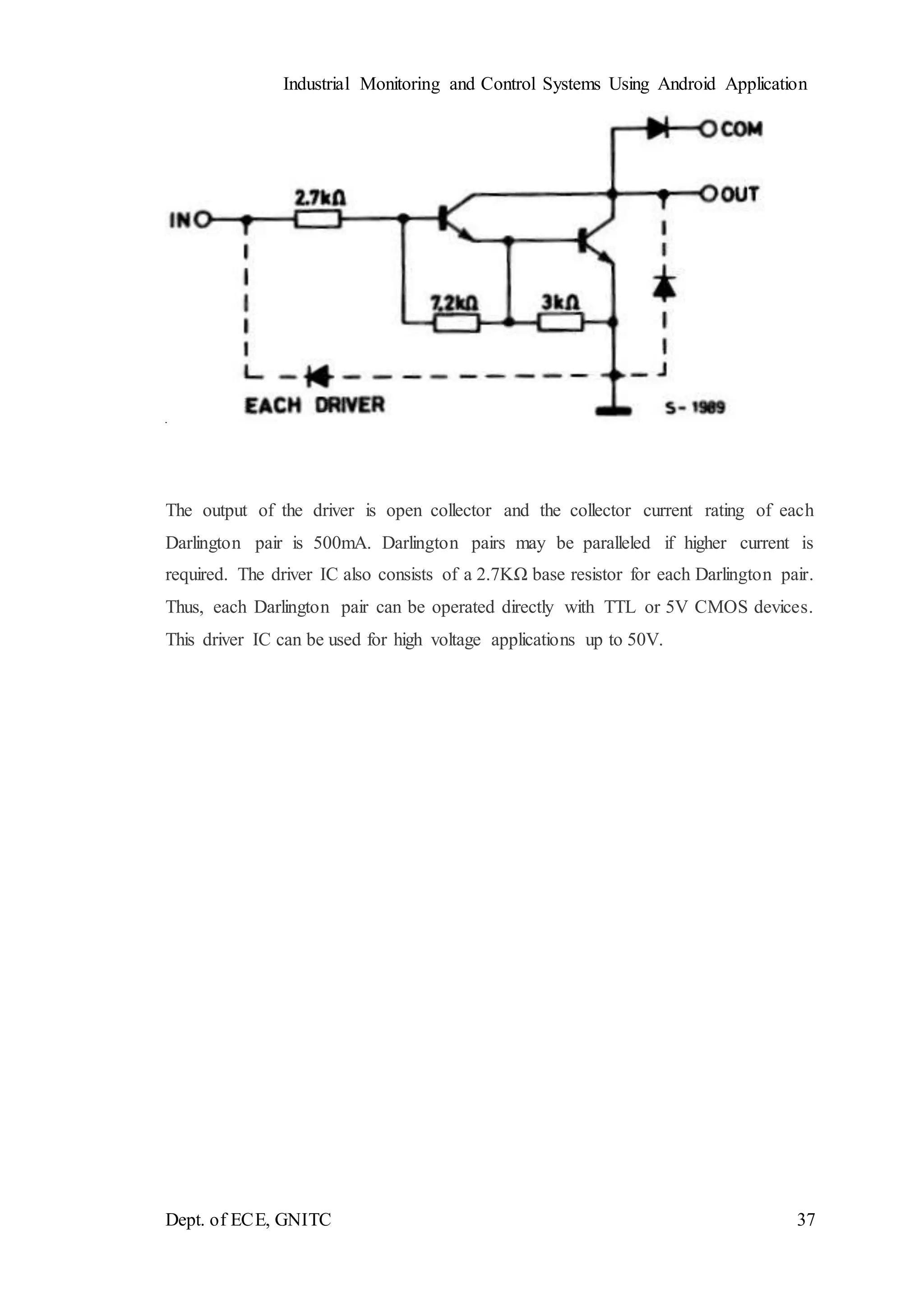
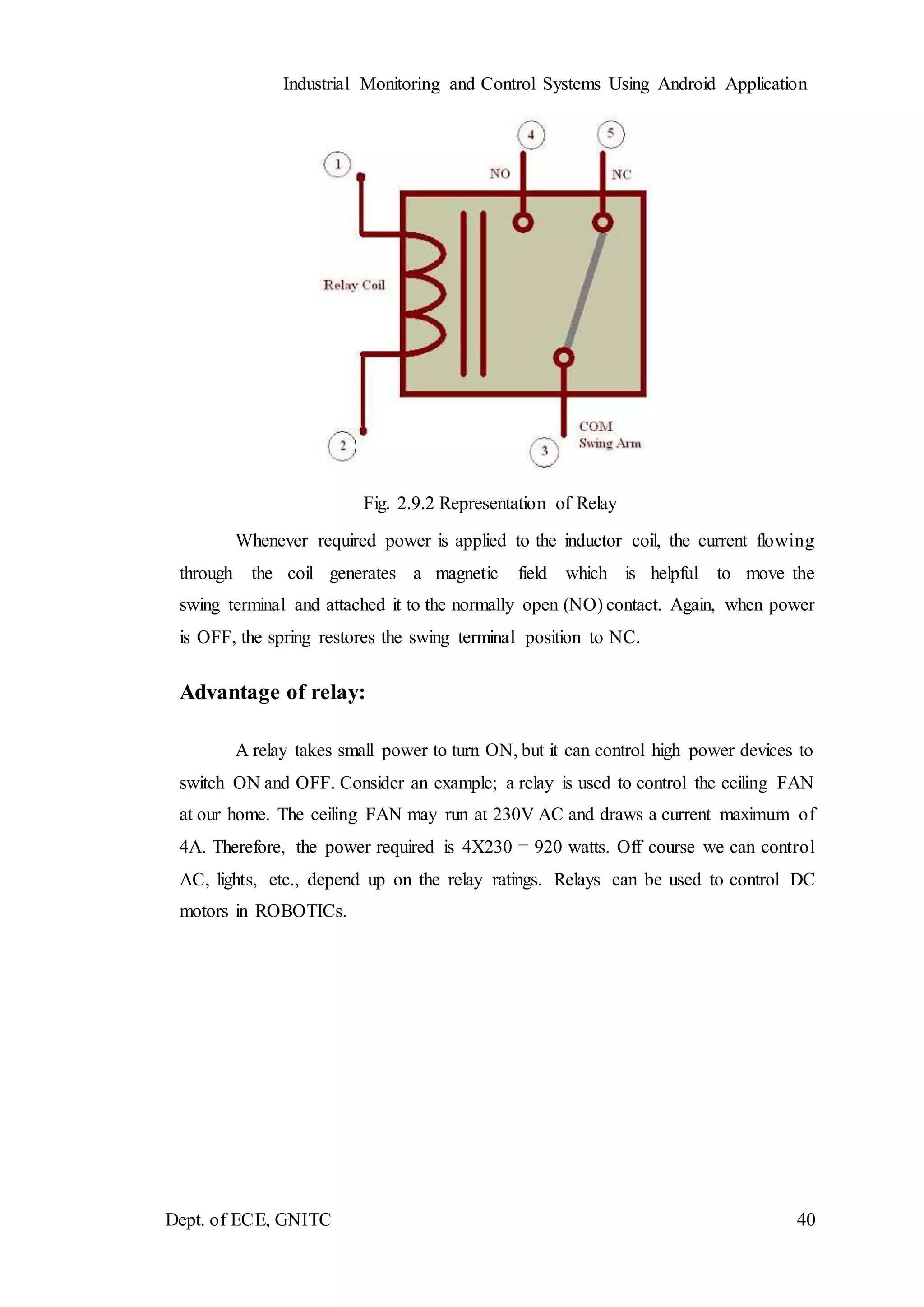
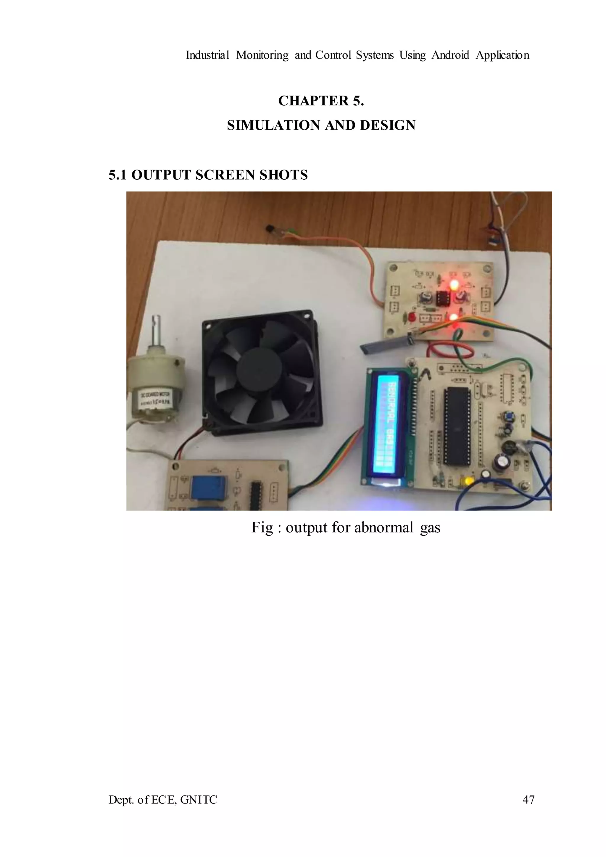
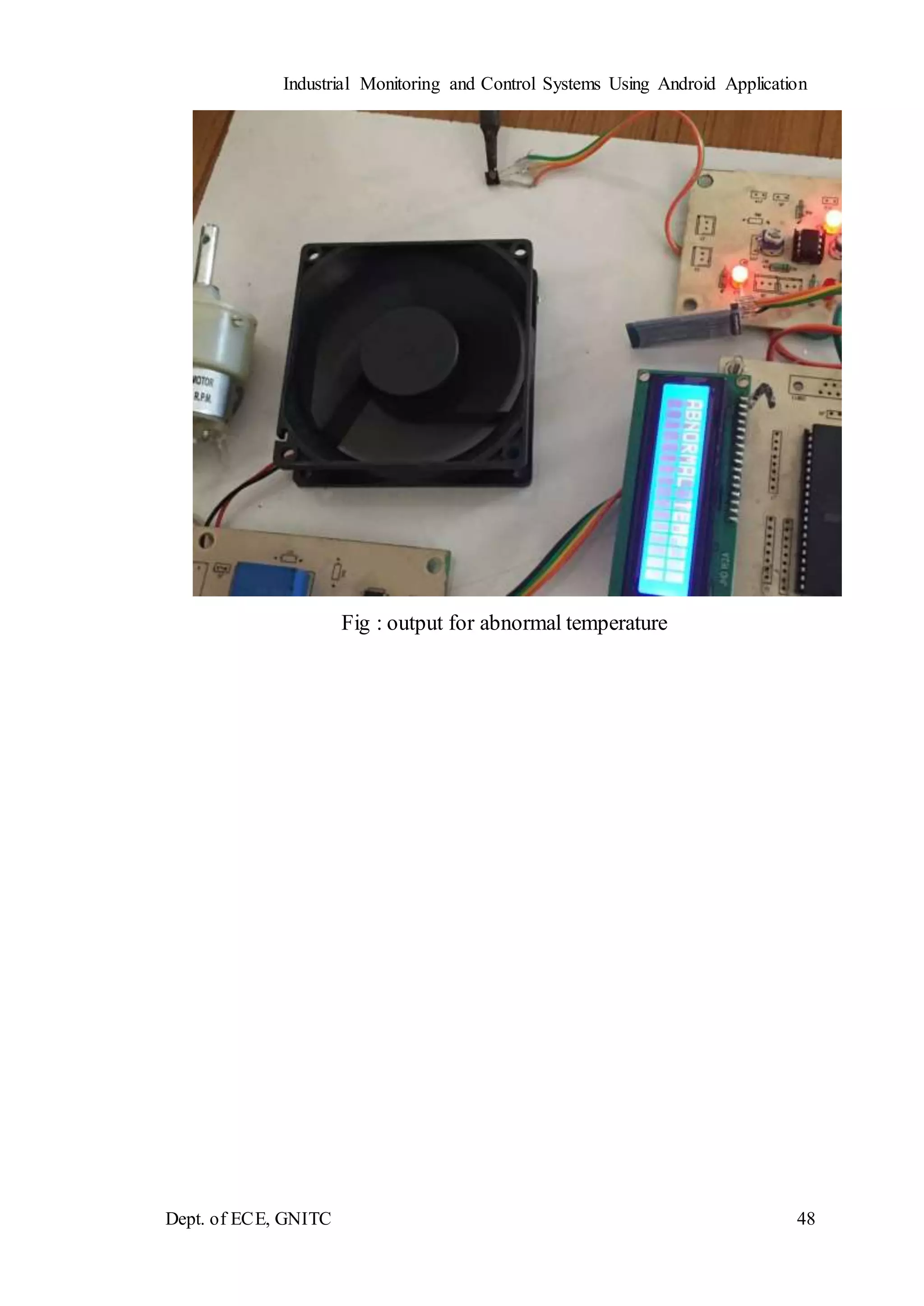
Industrial Monitoring and Control Systems Using Android Application
Dept. of ECE, GNITC 1
CHAPTER - 1
INTRODUCTION
1.1GENERAL
Wireless sensor networks (wsn) have been Employed to collect data about physical
phenomena in Various applications such as habitat monitoring, and ocean monitoring,
And surveillance. As an emerging technology Brought about rapid advances in modern
wireless telecommunication, Internet of Things (iot) has attracted a lot of attention and
Is expected to bring benefits to numerous application areas including Industrial wsn
systems, and healthcare systems manufacturing. WSN systems are well-suited for long-
term industrial Environmental data acquisition for iot representation. Sensor Interface
device is essential for detecting various kinds of sensor Data of industrial WSN in iot
environments. It enables us to acquire sensor data. Thus, we can better understand the
outside Environment information. However, in order to meet the requirements of long-
term industrial environmental data acquisition in the iot, the acquisition interface device
can collect multiple sensor Data at the same time, so that more accurate and diverse data
Information can be collected from industrial WSN.
1.2 OBJECTIVE
Today, the broad proliferation of Smart phones and Tablets has determined a
wide availability of software applications for numerous purposes. Thanks to this,
Smartphones are now essential devices for many aspects of everyday life and not just
advanced mobile phone terminals. The presence of powerful processing units,
embedded sensors as well as the availability of many standard communication interfaces
has recently attracted the interest of the scientific community. Several projects based on
Smartphone systems have been proposed in different fields and many more application
scenarios are being explored. A critical aspect still unresolved is the possibility of
acquiring external information, such as data from other sensors. Due to their nature of
consumer devices, Smartphones provide digital and high level communication
interfaces, such as USB and Bluetooth.
Industrial Monitoring and Control Systems Using Android Application
Dept. of ECE, GNITC 2
1.3 EXISTING SYSTEM:
Data logging is a process in which a controller is used to collect the process control
parameters with the help of sensors and analyze and store the results for further future
analysis. SCADA system is a high end current control system which is implemented in
all major automation industries.
1.4 DISADVANTAGES OF EXISTING SYSTEM
 There is no wireless system for data transfer.
 High cost and more time consumption.
1.5 PROPOSED SYSTEM
 In this system, the WBN is designed to monitor the status of the physical
parameters.
 While monitoring there is data updating is happened the system will send the
data to the monitoring section.
1.6ADVANTAGES OF PROPOSED SYSTEM
 It is used in military, sports and individual purpose.
 Low cost and wireless.
Industrial Monitoring and Control Systems Using Android Application
Dept. of ECE, GNITC 3
CHAPTER 2
PROJECT DESCRIPTION
2.1 INTRODUCTION TO EMBEDDED SYSTEM
An embedded system can be defined as a computing device that does a specific
focused job. Appliances such as the air-conditioner, VCD player, DVD player, printer,
fax machine, mobile phone etc. are examples of embedded systems. Each of these
appliances will have a processor and special hardware to meet the specific requirement
of the application along with the embedded software that is executed by the processor
for meeting that specific requirement. The embedded software is also called “firm
ware”. The desktop/laptop computer is a general-purpose computer. You can use it for
a variety of applications such as playing games, word processing, accounting, software
development and so on. In contrast, the software in the embedded systems is always
fixed listed below:
Embedded systems do a very specific task, they cannot be programmed to do different
things. Embedded systems have very limited resources, particularly the memory.
Generally, they do not have secondary storage devices such as the CDROM or the
floppy disk. Embedded systems have to work against some deadlines. A specific job has
to be completed within a specific time. In some embedded systems, called real-time
systems, the deadlines are stringent. Missing a deadline may cause a catastrophe-loss of
life or damage to property. Embedded systems are constrained for power. As many
embedded systems operate through a battery, the power consumption has to be very low.
Some embedded systems have to operate in extreme environmental conditions such as
very high temperatures and humidity.
Application Areas:
Nearly 99 per cent of the processors manufactured end up in embedded systems. The
embedded system market is one of the highest growth areas as these systems are used
in very market segment- consumer electronics, office automation, industrial
Industrial Monitoring and Control Systems Using Android Application
Dept. of ECE, GNITC 4
automation, biomedical engineering, wireless communication, data communication,
telecommunications, transportation, military and so on.
Now, let us see the details of the various building blocks of the hardware of an embedded
system. As shown in Fig. the building blocks are;
· Central Processing Unit (CPU)
· Memory (Read-only Memory and Random-Access Memory)
· Input Devices
· Output devices
· Communication interfaces
· Application-specific circuitry
Fig 2.1 Building Blocks of 8051
Central Processing Unit (CPU):
The Central Processing Unit (processor, in short) can be any of the following:
microcontroller, microprocessor or Digital Signal Processor (DSP). A micro-controller
is a low-cost processor. Its main attraction is that on the chip itself, there will be many
other components such as memory, serial communication interface, analog-to digital
converter etc. So, for small applications, a micro-controller is the best choice as the
number of external components required will be very less. On the other hand,
microprocessors are more powerful, but you need to use many external components with
Industrial Monitoring and Control Systems Using Android Application
Dept. of ECE, GNITC 5
them. DSP is used mainly for applications in which signal processing is involved such
as audio and video processing.
Memory:
The memory is categorized as Random-Access Memory (RAM) and Read Only
Memory (ROM). The contents of the RAM will be erased if power is switched off to
the chip, whereas ROM retains the contents even if the power is switched off. So, the
firmware is stored in the ROM. When power is switched on, the processor reads the
ROM; the program is program is executed.
Input devices:
Unlike the desktops, the input devices to an embedded system have very limited
capability. There will be no keyboard or a mouse, and hence interacting with the
embedded system is no easy task. Many embedded systems will have a small keypad-
you press one key to give a specific command. A keypad may be used to input only the
digits. Many embedded systems used in process control do not have any input device
for user interaction; they take inputs from sensors or transducers fnd produce electrical
signals that are in turn fed to other systems.
Output devices:
The output devices of the embedded systems also have very limited capability. Some
embedded systems will have a few Light Emitting Diodes (LEDs) to indicate the health
status of the system modules, or for visual indication of alarms. A small Liquid Crystal
Display (LCD) may also be used to display some important parameters.
Communication interfaces:
The embedded systems may need to, interact with other embedded systems at they may
have to transmit data to a desktop. To facilitate this, the embedded systems are provided
with one or a few communication interfaces such as RS232, RS422, RS485, Universal
Serial Bus (USB), IEEE 1394, Ethernet etc.
Industrial Monitoring and Control Systems Using Android Application
Dept. of ECE, GNITC 6
Application-specific circuitry:
Sensors, transducers, special processing and control circuitry may be required fat an
embedded system, depending on its application. This circuitry interacts with the
processor to carry out the necessary work. The entire hardware has to be given power
supply either through the 230 volts main supply or through a battery. The hardware has
to design in such a way that the power consumption is minimized.
2.2 Block Diagram:
Micro
controller
Temperature
sensor
ULN 2003
Gas sensor
Bluetooth
dongle
Relay Relay
Device
Device
Industrial Monitoring and Control Systems Using Android Application
Dept. of ECE, GNITC 7
2.3 MODULES
1. POWER SUPPLY
The power supply section is the section which provide +5V for the components
to work. IC LM7805 is used for providing a constant power of +5V.
The ac voltage, typically 220V, is connected to a transformer, which steps down
that ac voltage down to the level of the desired DC output. A diode rectifier then
provides a full-wave rectified voltage that is initially filtered by a simple capacitor filter
to produce a DC voltage. This resulting DC voltage usually has some ripple or AC
voltage variation.
A regulator circuit removes the ripples and also retains the same DC value even
if the input DC voltage varies, or the load connected to the output DC voltage changes.
This voltage regulation is usually obtained using one of the popular voltage regulator
IC units.
Fig. 2.3.1 Block Diagram of Power Supply
Transformer
Transformers convert AC electricity from one voltage to another with little loss
of power. Transformers work only with AC and this is one of the reasons why mains
electricity is AC.
Step-up transformers increase voltage, step-down transformers reduce voltage.
Most power supplies use a step-down transformer to reduce the dangerously high mains
voltage (230V in India) to a safer low voltage.
Industrial Monitoring and Control Systems Using Android Application
Dept. of ECE, GNITC 8
The input coil is called the primary and the output coil is called the secondary.
There is no electrical connection between the two coils; instead they are linked by an
alternating magnetic field created in the soft-iron core of the transformer. Transformers
waste very little power so the power out is (almost) equal to the power in. Note that as
voltage is stepped down current is stepped up. The transformer will step down the power
supply voltage (0-230V) to (0- 6V) level. Then the secondary of the potential
transformer will be connected to the bridge rectifier, which is constructed with the help
of PN junction diodes. The advantages of using bridge rectifier are it will give peak
voltage output as DC.
Rectifier
There are several ways of connecting diodes to make a rectifier to convert
AC to DC. The bridge rectifier is the most important and it produces full-wave varying
DC. A full-wave rectifier can also be made from just two diodes if a center-tap
transformer is used, but this method is rarely used now that diodes are cheaper. A single
diode can be used as a rectifier but it only uses the positive (+) parts of the AC wave to
produce half-wave varying DC.
Bridge Rectifier
When four diodes are connected as shown in figure, the circuit is called as bridge
rectifier. The input to the circuit is applied to the diagonally opposite corners of the
network, and the output is taken from the remaining two corners. Let us assume that the
transformer is working properly and there is a positive potential, at point A and a
negative potential at point B. the positive potential at point A will forward bias D3 and
reverse bias D4.
Fig. 2.3.2 Bridge Rectifier
Industrial Monitoring and Control Systems Using Android Application
Dept. of ECE, GNITC 9
The negative potential at point B will forward bias D1 and reverse D2. At this time D3
and D1 are forward biased and will allow current flow to pass through them; D4 and D2
are reverse biased and will block current flow.
One advantage of a bridge rectifier over a conventional full-wave rectifier is that with a
given transformer the bridge rectifier produces a voltage output that is nearly twice that
of the conventional full-wave circuit.
i. The main advantage of this bridge circuit is that it does not require a special center
tapped transformer, thereby reducing its size and cost.
ii. The single secondary winding is connected to one side of the diode bridge network
and the load to the other side as shown below.
iii. The result is still a pulsating direct current but with double the frequency.
Fig. 2.3.3 Output Waveform of DC
Smoothing
Smoothing is performed by a large value electrolytic capacitor connected across
the DC supply to act as a reservoir, supplying current to the output when the varying
DC voltage from the rectifier is falling. The capacitor charges quickly near the peak of
the varying DC, and then discharges as it supplies current to the output.
Industrial Monitoring and Control Systems Using Android Application
Dept. of ECE, GNITC 10
Voltage Regulators
Voltage regulators comprise a class of widely used ICs. Regulator IC units
contain the circuitry for reference source, comparator amplifier, control device, and
overload protection all in a single IC. IC units provide regulation of either a fixed
positive voltage, a fixed negative voltage, or an adjustably set voltage. The regulators
can be selected for operation with load currents from hundreds of milli amperes to tens
of amperes, corresponding to power ratings from milli watts to Tens of watts.
A fixed three-terminal voltage regulator has an unregulated dc input voltage, Vi,
applied to one input terminal, a regulated dc output voltage, Vo, from a second terminal,
with the third terminal connected to ground.
The series 78 regulators provide fixed positive regulated voltages from 5 to 24
volts. Similarly, the series 79 regulators provide fixed negative regulated voltages from
5 to 24 volts. Voltage regulator ICs are available with fixed (typically 5, 12 and 15V) or
variable output voltages. They are also rated by the maximum current they can pass.
Negative voltage regulators are available, mainly for use in dual supplies. Most
regulators include some automatic protection from excessive current ('overload
protection') and overheating ('thermal protection').
Many of the fixed voltage regulator ICs has 3 leads and look like power
transistors, such as the 7805 +5V 1Amp regulator. They include a hole for attaching a
heat sink if necessary.
Fig. 2.3.4 Regulator
Industrial Monitoring and Control Systems Using Android Application
Dept. of ECE, GNITC 11
Fig. 2.3.5 Circuit Diagram of Power Supply
2.4. MICROCONTROLLER
A Microcontroller (or MCU) is a computer-on-a-chip used to control electronic devices.
It is a type of microprocessor emphasizing self-sufficiency and cost-effectiveness, in
contrast to a general-purpose microprocessor (the kind used in a PC). A typical
microcontroller contains all the memory and interfaces needed for a simple application,
whereas a general-purpose microprocessor requires additional chips to provide these
functions.
A microcontroller is a single integrated circuit with the following key features:
central processing unit - ranging from small and simple 8-bit processors to sophisticated
32- or 64-bit processors
input/output interfaces such as serial ports
RAM for data storage
ROM, EEPROM or Flash memory for program storage
clock generator - often an oscillator for a quartz timing crystal, resonator or RC circuit
Microcontrollers are inside many kinds of electronic equipment (see embedded system).
They are the vast majority of all processor chips sold. Over 50% are "simple"
controllers, and another 20% are more specialized digital signal processors (DSPs)
(ref?). A typical home in a developed country is likely to have only one or two general-
purpose microprocessors but somewhere between one and two dozen microcontrollers.
A typical mid-range vehicle has as many as 50 or more microcontrollers. They can also
Industrial Monitoring and Control Systems Using Android Application
Dept. of ECE, GNITC 12
be found in almost any electrical device: washing machines, microwave ovens,
telephones etc.
2.4.1 MICROCONTROLLER
FEATURES
• Compatible with MCU®-51 Products
• 8K Bytes of In-System Programmable (ISP) Flash Memory – Endurance: 10,000
Write/Erase Cycles
• 4.0V to 5.5V Operating Range
• Fully Static Operation: 0 Hz to 33 MHz
• 256 x 8-bit Internal RAM
• 32 Programmable I/O Lines
• Three 16-bit Timer/Counters
• Eight Interrupt Sources
• Full Duplex UART Serial Channel
• Low-power Idle and Power-down Modes
• Interrupt Recovery from Power-down Mode
• Fast Programming Time
• Flexible ISP Programming (Byte and Page Mode)
Description
The AT89S52 is a low-power, high-performance CMOS 8-bit microcontroller
with 8K bytes of in-system programmable Flash memory. The device is manufactured
using Atmel’s high-density nonvolatile memory technology and is compatible with the
industry-standard 80C51 instruction set and pin-out. The on-chip Flash allows the
program memory to be reprogrammed in-system or by a conventional nonvolatile
Industrial Monitoring and Control Systems Using Android Application
Dept. of ECE, GNITC 13
memory programmer. By combining a versatile 8-bit CPU with in-system
programmable Flash on a monolithic chip, the Atmel AT89S52 is a powerful
microcontroller which provides a highly-flexible and cost-effective solution to many
embedded control applications.
The AT89S52 provides the following standard features: 8K bytes of Flash, 256
bytes of RAM, 32 I/O lines, three 16-bit timer/counters, a six-vector two-level interrupt
architecture, a full duplex serial port, on-chip oscillator, and clock circuitry. In addition,
the AT89S52 is designed with static logic for operation down to zero frequency and
supports two software selectable power saving modes. The Idle Mode stops the CPU
while allowing the RAM, timer/counters, serial port, and interrupt system to continue
functioning. The Power-down mode saves the RAM con-tents but freezes the oscillator,
disabling all other chip functions until the next interrupt or hardware reset.
Fig. 2.4.1 BLOCK DIAGRAM OF 8051
Industrial Monitoring and Control Systems Using Android Application
Dept. of ECE, GNITC 14
PIN DIAGRAM
Fig. 2.4.2 PIN DIAGRAM OF 8051
PIN DESCRIPTION
40 pin VCC Supply voltage.
20 pin GND Ground.
Port 0
Port 0 is an 8-bit open drain bidirectional I/O port. As an output port, each pin can sink
eight TTL inputs. When 1s are written to port 0 pins, the pins can be used as high-
impedance inputs. Port 0 can also be configured to be the multiplexed low-order
address/data bus during accesses to external program and data memory. Port 0 also
receives the code bytes during Flash programming and outputs the code bytes during
program verification. External pull-ups are required during program verification.
Industrial Monitoring and Control Systems Using Android Application
Dept. of ECE, GNITC 15
Port 1
Port 1 is an 8-bit bidirectional I/O port with internal pull-ups. The Port 1 output buffers
can sink/source four TTL inputs. When 1s are written to Port 1 pins, they are pulled high
by the internal pull-ups and can be used as inputs. As inputs, Port 1 pins that are
externally being pulled low will source current (IIL) because of the internal pull-ups.
Port 2
Port 2 is an 8-bit bidirectional I/O port with internal pull-ups. The Port 2 output buffers
can sink/source four TTL inputs. When 1s are written to Port 2 pins, they are pulled high
by the internal pull-ups and can be used as inputs. As inputs, Port 2 pins that are
externally being pulled low will source current because of the internal pull-ups. In this
application, Port 2 uses strong internal pull-ups when emitting 1s. During accesses to
external data memory that use 8-bit addresses, Port 2 emits the contents of the P2 Special
Function Register. Port 2 also receives the high-order address bits and some control
signals during Flash programming and verification.
Port 3
Port 3 is an 8-bit bidirectional I/O port with internal pull-ups. The Port 3 output buffers
can sink/source four TTL inputs. When 1s are written to Port 3 pins, they are pulled high
by the internal pull-ups and can be used as inputs. As inputs, Port 3 pins that are
externally being pulled low will source current because of the pull-ups. Port 3 also
serves the functions of various special features of the AT89S52, as shown in the
following table.
Table No 2.4.1 Pin Description
Industrial Monitoring and Control Systems Using Android Application
Dept. of ECE, GNITC 16
RST
Reset input. A high on this pin for two machine cycles while the oscillator is running
resets the device.
WR
It is active low write O/P control signal. During External RAM (Data memory). Write
to external RAM.
RD
It is active low read O/P control signal. During External RAM (Data memory). Read
from External RAM.
XTAL1
Input to the inverting oscillator amplifier and input to the internal clock operating circuit.
XTAL2
Output from the inverting oscillator amplifier.
ALE/PROG
Address Latch Enable (ALE) is an output pulse for latching the low byte of the address
during accesses to external memory. This pin is also the program pulse input (PROG)
during Flash programming. In normal operation, ALE is emitted at a constant rate of 1/6
the oscillator frequency and may be used for external timing or clocking purposes. If
desired, ALE operation can be disabled by setting bit 0 of SFR location 8EH. With the
bit set, ALE is active only during a MOVX or MOVC instruction. Otherwise, the pin is
weakly pulled high. Setting the ALE-disable bit has no effect if the microcontroller is
in external execution mode.
Industrial Monitoring and Control Systems Using Android Application
Dept. of ECE, GNITC 17
PSEN
Program Store Enable (PSEN) is the read strobe to external program memory. When the
AT89S52 is executing code from external program memory, PSEN is activated twice
each machine cycle.
EA
External Access Enable. EA must be strapped to GND in order to enable the device to
fetch code from external program memory locations starting at 0000H up to FFFFH.
Note, however, that if lock bit 1 is programmed, EA will be internally latched on reset.
EA should be strapped to VCC for internal program executions.
REGISTERS
Registers and accumulators serve as temporary memory locations during CPU
operations. The exchange of information among them takes place through one or more
internal buses. The length of each register is equal to the width of the internal data bus.
Registers are categorized as general-purpose registers and special-purpose registers.
A general-purpose register may be used as an accumulator or as a data register
for (arithmetic) and logic operations. An accumulator is a register for storing the results
of an arithmetic operation. A general-purpose register may also be used as an address
register.
A special-purpose register is dedicated to a specific function. Some of these registers
are the program counter (PC), the instruction register (IR), the address register (AR),
the status register, and the stack pointer (SP).
The program counter holds the address of the next instruction to be executed.
When the CPU executes a branch, instruction telling it to branch to another part of the
program, the new address is loaded into the program counter and the sequential order
resumes.
The instruction register extracts the operation code (op code) from an
instruction. An instruction consists of op code and operand(s). The contents of the
Industrial Monitoring and Control Systems Using Android Application
Dept. of ECE, GNITC 18
instruction register are decoded by the control unit. The status register or condition code
register consists of status or flag bits and control bits.
The flag bits are: carry/borrow (C), overflow (V), negative (N), zero (Z), and
half-carry (H). The logic states of the flag bits are used by the CPU’s branch instructions
to make decisions. The program counter sends its contents (address) to the address
register. The address register then sends this address to the address bus.
A stack is a specially reserved area in memory where information is stored or
removed in a last-in-first-out (LIFO) fashion. The stack pointer points to the next free
location on the stack. That is, it holds the address of the top of the stack. Each time data
is stored in the stack, the stack pointer is automatically decremented and each time data
is retrieved from the stack, the stack pointer is automatically incremented.
Memory Organization
MCU-51 devices have a separate address space for Program and Data Memory. Up to
64K bytes each of external Program and Data Memory can be addressed.
The instructions to be executed by the microcontroller CPU and the data to be
operated on by these instructions are stored in memory. When the CPU accesses the
information stored in memory, it is performing a read operation. When the CPU sends
information to be stored in the memory, it is performing a write operation. Memory is
classified as internal and external memory. Internal memory is on-chip memory and is
a semiconductor type with low capacity and high speeds. External memory is outside
the chip and includes the semiconductor type and serial memory such as magnetic disks,
magnetic tapes, and bubble memory. Semiconductor memory may be volatile or
nonvolatile. Volatile memory loses its contents after the power is removed from the
memory chip. Nonvolatile memory does not lose its contents when power is removed.
The nonvolatile memory can store information permanently or at least semi-
permanently (ten years or more). Volatile memory includes RAM while nonvolatile
memory includes ROM, EPROM, EEPROM, and battery-backed RAM.
RAM (random access memory) comprises DRAM (Dynamic RAM) and SRAM
(Static RAM). Each storage cell of DRAM consists of a capacitor and a MOSFET
(Metal Oxide Semiconductor Field Effect Transistor). If the capacitor is charged, a logic
Industrial Monitoring and Control Systems Using Android Application
Dept. of ECE, GNITC 19
1 is stored in the cell. If the capacitor has no charge, a logic 0 is stored in the cell. The
charge stored in the capacitors dissipates fast because of leakage. Therefore, a DRAM
has to be periodically refreshed otherwise its contents will fade away after some time
even in the presence of the power to memory chip.
The storage cell of a ROM (Read-only memory) consists of a BJT (Bipolar
Junction Transistor). A ROM may be programmed at the manufacturing stage using a
mask process. Such a ROM is called mask-programmed ROM. The contents of a mask-
programmed ROM cannot be changed once it is programmed.
UART (Universal Asynchronous Receiver and Transmitter)
One of the microcontroller features making it so powerful is an integrated UART, better
known as a serial port. It is a full-duplex port, thus being able to transmit and receive
data simultaneously and at different baud rates. Without it, serial data send and receive
would be an enormously complicated part of the program in which the pin state is
constantly changed and checked at regular intervals. When using UART, all the
programmer has to do is to simply select serial port mode and baud rate. When it's done,
serial data transmit is nothing but writing to the SBUF register, while data receive
represents reading the same register. The microcontroller takes care of not making any
error during data transmission.
TIMERS
Timer is use to generate time delay; a timer always counts up. It doesn’t matter whether
the timer is being used as a timer, a counter, or a baud rate generator: A timer is always
incremented by the microcontroller. There are 3 timers i.e., Timer 0, Timer 1 and Timer
2.
Timer 0 and 1
Timer 0 and Timer 1 in the AT89S52 operate the same way as Timer 0 and Timer 1 in
the 8051. Timer T0 is a 16-bit timer. The 16-bit Timer 0 is accessed as low byte and
high byte. the low byte is called TL0(Timer 0 low byte) and the high byte is referred to
as TH0(Timer 0 high byte). As like Timer 1 is also 16-bit timer is split into two bytes,
Industrial Monitoring and Control Systems Using Android Application
Dept. of ECE, GNITC 20
referred to as TL1 (Timer 1 low byte) and TH1(Timer 1 high byte). These timers are
accessible in the same way as the Timer 0.
Timer 2
Timer 2 is a 16-bit Timer/Counter that can operate as either a timer or an event counter.
The type of operation is selected by bit C/T2 in the SFR T2CON (shown in Table 5-2).
Timer 2 has three operating modes: capture, auto-reload (up or down counting), and
baud rate generator. Timer 2 consists of two 8-bit registers, TH2 and TL2. In the Timer
function, the TL2 register is incremented every machine cycle. Since a machine cycle
consists of 12 oscillator periods, the count rate is 1/12 of the oscillator frequency.
In the Counter function, the register is incremented in response to a 1-to-0 transition at
its corresponding external input pin, T2. In this function, the external input is sampled
during S5P2 of every machine cycle. When the samples show a high in one cycle and a
low in the next cycle, the count is incremented. The new count value appears in the
register during S3P1 of the cycle following the one in which the transition was detected.
Since two machine cycles (24 oscillator periods) are required to recognize a 1-to-0
transition, the maximum count rate is 1/24 of the oscillator frequency. To ensure that a
given level is sampled at least once before it changes, the level should be held for at
least one full machine cycle.
INTERRUPTS
The AT89S52 has a total of six interrupt vectors: two external interrupts (INT0 and
INT1), three timer interrupts (Timers 0, 1, and 2), and the serial port interrupt.
Each of these interrupt sources can be individually enabled or disabled by setting or
clearing a bit in Special Function Register IE. IE also contains a global disable bit, EA,
which disables all interrupts at once.
Timer 2 interrupt is generated by the logical OR of bits TF2 and EXF2 in register
T2CON. Neither of these flags is cleared by hardware when the service routine is
vectored to. In fact, the service routine may have to determine whether it was TF2 or
EXF2 that generated the interrupt, and that bit will have to be cleared in software. The
Timer 0 and Timer 1 flags, TF0 and TF1, uses the cycle in which the timers overflow.
Industrial Monitoring and Control Systems Using Android Application
Dept. of ECE, GNITC 21
The values are then polled by the circuitry in the next cycle. However, the Timer 2 flag,
TF2, is set at S2P2 and is polled in the same cycle in which the timer overflows.
2.5(a) Serial communication:
When using the serial communication, we transmit the multi-bit word bit after
bit (when at any given moment only one bit will pass).
2.5(b) Parallel communication:
When using the parallel communication, however, the number of bits will be
transmitted at once from one computer to the second computer.
In addition to the serial and parallel communications, there are 2 types of
communication we will explore:
Industrial Monitoring and Control Systems Using Android Application
Dept. of ECE, GNITC 22
 Synchronous communication
 Asynchronous communication
Synchronous communication
When using the synchronous communication – the information is transmitted
from the transmitter to the receiver:
 in sequence
 bit after bit
 with fixed baud rate
 and the clock frequency is transmitted along with the bits
Asynchronous communication
When using the asynchronous communication - the transmitter and the receiver
refraining to transmit long sequences of bits because there isn't a full synchronization
between the transmitter, that sends the data, and the receiver, that receives the data.
In this case, the information is divided into frames, in the size of byte. Each one of the
frame has:
 “Start” bit marks the beginning of a new frame.
 “Stop” bit marks the end of the frame.
CRYSTAL OSCILLATOR
The 8051 uses the crystal for precisely that: to synchronize its operation. Effectively,
the 8051 operates using what are called "machine cycles." A single machine cycle is the
minimum amount of time in which a single 8051 instructions can be executed. Although
many instructions take multiple cycles. 8051 has an on-chip oscillator. It needs an
external crystal that decides the operating frequency of the 8051. The crystal is
connected to pins 18 and 19 with stabilizing capacitors. 12 MHz (11.059MHz) crystal
is often used and the capacitance ranges from 20pF to 40pF. A cycle is, in reality, 12
Industrial Monitoring and Control Systems Using Android Application
Dept. of ECE, GNITC 23
pulses of the crystal. That is to say, if an instruction takes one machine cycle to execute,
it will take 12 pulses of the crystal to execute. Since we know the we can calculate how
many instructions cycles the 8051 can execute per second:
11,059,000 / 12 = 921,583
11.0592 MHz crystals are often used because it can be divided to give you exact clock
rates for most of the common baud rates for the UART, especially for the higher speeds
(9600, 19200).
Reset
RESET is an active High Input When RESET is set to High, 8051 goes back to the
power on state. The 8051 is reset by holding the RST high for at least two machine
cycles and then returning it low. Initially charging of capacitor makes RST High, when
capacitor charges fully it blocks DC.
Industrial Monitoring and Control Systems Using Android Application
Dept. of ECE, GNITC 24
LIQUID CRYSTAL DISPLAY (LCD)
LCD (Liquid Crystal Display) screen is an electronic display module and find a
wide range of applications. A 16x2 LCD display is very basic module and is very
commonly used in various devices and circuits. These modules are preferred over seven
segments and other multi segment LEDs. The reasons being: LCDs are economical;
easily programmable; have no limitation of displaying special & even custom characters
(unlike in seven segments), animations and so on.
A 16x2 LCD means it can display 16 characters per line and there are 2 such
lines. In this LCD, each character is displayed in 5x7 pixel matrix. This LCD has two
registers, namely, Command and Data.
The command register stores the command instructions given to the LCD. A
command is an instruction given to LCD to do a predefined task like initializing it,
clearing its screen, setting the cursor position, controlling display etc. The data register
stores the data to be displayed on the LCD. The data is the ASCII value of the character
to be displayed on the LCD.
Fig. 2.4.3 16x2 LCD
Introduction
The most commonly used Character based LCDs are based on Hitachi's
HD44780 controller or other which are compatible with HD44580.
Industrial Monitoring and Control Systems Using Android Application
Dept. of ECE, GNITC 25
Pin Description
Most LCDs with 1 controller has 14 Pins and LCDs with 2 controller has 16 Pins
(two pins are extra in both for back-light LED connections). Pin description is shown in
the table below.
Pin Configuration table for a 16X2 LCD character display:-
Pin Number Symbol Function
1 VSS Ground Terminal
2 Vcc Positive Supply
3 VDD Contrast adjustment
4 RS Register Select; 0→Instruction Register, 1→Data Register
5 R/W Read/write Signal; 1→Read, 0→ Write
6 E Enable; Falling edge
7 DB0
Bi-directional data bus, data transfer is performed once, thru
DB0 to DB7, in the case of interface data length is 8-bits; and
twice, through DB4 to DB7 in the case of interface data length
is 4-bits. Upper four bits first then lower four bits.
8 DB1
9 DB2
10 DB3
11 DB4
12 DB5
13 DB6
14 DB7
15 LED-(K) Back light LED cathode terminal
16 LED+(A) Back Light LED anode terminal
Table No 2.4.2 :Pin Description Of LCD
Liquid crystal displays interfacing with Controller
The LCD standard requires 3 control lines and 8 I/O lines for the data bus.
Industrial Monitoring and Control Systems Using Android Application
Dept. of ECE, GNITC 26
• 8 data pins D7:D0
Bi-directional data/command pins.
Alphanumeric characters are sent in ASCII format.
• RS: RegisterSelect
RS = 0 Command Register is selected
RS = 1 Data Register is selected
• R/W: Read or Write
0 - Write, 1 - Read
• E: Enable (Latch data)
Used to latch the data present on the data pins. A high-to-low edge is needed to
latch the data.
2.5. TEMPERATURE SENSOR
Temperature is the most-measured process variable in industrial automation.
Most commonly, a temperature sensor is used to convert temperature value to an
electrical value. Temperature Sensors are the key to read temperatures correctly and to
control temperature in industrials applications.
A large distinction can be made between temperature sensor types. Sensors
differ a lot in properties such as contact-way, temperature range, calibrating method and
sensing element. The temperature sensors contain a sensing element enclosed in
housings of plastic or metal. With the help of conditioning circuits, the sensor will
reflect the change of environmental temperature.
Industrial Monitoring and Control Systems Using Android Application
Dept. of ECE, GNITC 27
Temperature sensor (LM35)
Pin Definition
The definition of gray-scale sensor pin is
1. Signal Output
2. GND
3. Power
Features of Temperature Sensor
 Calibrated directly in Celsius (centigrade)
 0.50 C Ensured accuracy (at +250 C)
 Suitable for remote applications
 Operate from 4 to 30 V
 Low cost due to wafer-level trimming
Specifications
 Type: Analog
 Sensitivity: 10mV per degree Celsius
 Functional range: 0 degree Celsius to 100 degrees Celsius
Industrial Monitoring and Control Systems Using Android Application
Dept. of ECE, GNITC 28
Description
The LM35 series are precision integrated-circuit temperature sensors, with an
output voltage linearly proportional to the Centigrade temperature. Thus, LM35 has an
advantage over linear temperature sensors calibrated in ° Kelvin, as the user is not
required to subtract a large constant voltage from the output to obtain convenient
Centigrade scaling.
In the temperature functional module, we developed, we use the LM34 series of
temperature sensors. The LM34 series are precision integrated-circuit temperature
sensors, whose output voltage is linearly proportional to the Fahrenheit temperature.
The LM34 thus has an advantage over linear temperature sensors calibrated in degrees
Kelvin, as the user is not required to subtract a large constant voltage from its output to
obtain convenient Fahrenheit scaling. The LM34 does not require any external
calibration or trimming to provide typical accuracies of ±1.2°F at room temperature and
±11.2°F over a full -50 to +300°F temperature range. The LM34 is rated to operate over
a -50° to +300°F temperature range.
+5V
GND
GND
OUTPUT
LM34
Figure 2.4.4 Circuit diagram for the LM34 temperature sensor functional module
It is easy to include the LM34 series in a temperature measuring application. The
output voltage of LM34 is linearly proportional to the Fahrenheit temperature, it has a
Linear +10.0 mV/°F scale factor which means that you will get n*10.0 mV output
voltage if the environment temperature is n°F.
The LM34 series is available packaged in hermetic TO-46 transistor packages,
while the LM34C, LM34CA and LM34D are also available in the plastic TO-92
transistor package. The LM34D is also available in an 8-lead surface mount small
outline package. In our functional module, LM34H in metal can package (TO-46) is
Industrial Monitoring and Control Systems Using Android Application
Dept. of ECE, GNITC 29
used in the functional module, it is very important to know that the wiring of sensor
should be based on the positions of the leading pins in different packages.
Figure 2.4.5 Package Diagram of LM34
DESCRIPTION OF TEMPERATURE SENSOR FUNCTIONAL MODULE
The temperature sensor functional module consists of two parts: the function
module box and the probe head. The LM34 temperature sensor is mounted on the probe
head. Be careful to make sure that the sensor is properly mounted on the probe head.
(refer to Figure 4 Labeled picture of the probe head.)
Figure 2.4.6Labeled picture of the temperature sensor circuit functional module.
Industrial Monitoring and Control Systems Using Android Application
Dept. of ECE, GNITC 30
By replacing the LM34 with another precision integrated-circuit temperature
sensor LM35, we can easily get an output voltage proportional to the centigrade
temperature. The LM35 sensor has a linear +10.0 mV/°C scale factor and a temperature
range from -55°C to +150°C.In fact LM34 and LM35 are among the same series of
temperature sensors so that they can be easily exchanged in different applications. The
wiring for LM 35 is the same as that of LM34. Please refer to the datasheets of LM34
and LM35 for more detailed packaging and features information
APPLICATIONS
The LM35 is applied easily in the same way as other integrated-circuit
temperature sensors. Glue or cement the device to a surface and the temperature should
be within about 0.01°C of the surface temperature.
This presumes that the ambient air temperature is almost the same as the surface
temperature. If the air temperature were much higher or lower than the surface
temperature, the actual temperature of the LM35 die would be at an intermediate
temperature between the surface temperature and the air temperature, which is
especially true for the TO-92 plastic package where the copper leads are the principal
thermal path to carry heat into the device, so its temperature might be closer to the air
temperature than to the surface temperature.
To minimize this problem, ensure that the wiring to the LM35, as it leaves the
device, is held at the same temperature as the surface of interest. The easiest way to do
this is to cover up these wires with a bead of epoxy which will insure that the leads and
wires are all at the same temperature as the surface, and that the temperature of the
LM35 die is not affected by the air temperature.
2.6 GAS SENSOR
Gas sensors are chemical sensors that are of paramount importance. A chemical
sensor comprises of a transducer and an active layer for converting the chemical
information into another form of electronic signal like frequency change, current
change or voltage change.
Industrial Monitoring and Control Systems Using Android Application
Dept. of ECE, GNITC 31
As the air surrounding us contains different amount of gases which could be
hazardous to human health, atmospheric pollutants or of significance to an industrial
or medical process, It becomes therefore very imperative to detect the presence of
these gases since the environment we dwell in consists of humans, plants and animals
as its main inhabitants, so the safety of their lives is of topmost priority.
Basically, traditional detection methods which produce systems that sounds an
audio alarm to notify people when there is a gas leakage that is harmful or poisonous
is not very reliable because it is required to obtain accurate real-time measurements of
the concentration of a target gas. However, for many centuries, different gas sensor
technologies have been used for different gases detection including semiconductor gas
sensors, catalytic gas sensors, electrochemical gas sensors, optical gas sensors and
acoustic gas sensors. The performance characteristic of every sensor is based on some
properties including sensitivity, selectivity, detection limit, response time and recovery
time.
Pin Definition
1. Signal Output
2. GND
3. Power
Industrial Monitoring and Control Systems Using Android Application
Dept. of ECE, GNITC 32
Features of Gas Sensor
 High sensitivity to LPG, Iso-butane, Propane
 Small sensitivity to alcohol and smoke
 Detection range 10-10000 ppm
 Fast response time <10sec
 Simple drive circuit and long life
 Heater voltage :5.0 V
2.7 BLUE TOOTH MODULE
Bluetooth is a wireless technology standard for exchanging data over short
distances (using short-wavelength UHF radio waves in the ISM band from 2.4 to 2.485
GHz) from fixed and mobile devices and building personal area networks (PANs). In
1994 a group of engineers at Ericsson, a Swedish company, invented a wireless
communication technology, later called Bluetooth. In 1998, the original group of
Promoter companies—Ericsson, Intel, Nokia, Toshiba and IBM—came together to form
the Bluetooth Special Interest Group (SIG).
Bluetooth networking transmits data via low-power radio waves. It
communicates on a frequency of 2.45 gigahertz (actually between 2.402 GHz and 2.480
GHz, to be exact). This frequency band has been set aside by international agreement
for the use of industrial, scientific and medical devices (ISM). By comparison, the most
powerful cell phones can transmit a signal of 3 watts. The low power limits the range of
a Bluetooth device to about 10 meters (32 feet), cutting the chances of interference
between your computer system and your portable telephone or television.
Some specification of Bluetooth
• Operates in the 2.4 GHZ band which is globally available
• It has 79 channels
• Uses FHSS, GFSK modulation
• 1600 hops per second
• Can support up to 8 devices in a piconet
• Omni-directional, non-line of sight transmission through walls
• 10m to 100m range
Industrial Monitoring and Control Systems Using Android Application
Dept. of ECE, GNITC 33
• Low cost, $20
• 1mW power
• Extended range with external power amplifier (100 meters)
BLUETOOTH MODULE
Baseband - There are two basic types of physical links that can be established between
a master and a slave:
 Synchronous Connection Oriented (SCO)
 Asynchronous Connection-Less (ACL)
An SCO link provides a symmetric link between the master and the slave, with
regular periodic exchange of data in the form of reserved slots. Thus, the SCO link
provides a circuit-switched connection where data are regularly exchanged, and as such
it is intended for use with time-bounded information as audio. A master can support up
to three SCO links to the same or to different slaves. A slave can support up to three
SCO links from the same master.
An ACI link is a point-to-multipoint link between the master and all the slaves on
the piconet. It can use all of the remaining slots on the channel not used for SCO links.
The ACL link provides a packet-switched connection where data are exchanged
sporadically, as they become available from higher layers of the stack. The traffic over
the ACL link is completely scheduled by the master.
Each Bluetooth device has a 48-bit IEEE MAC address that is used for the
derivation of the access code. The access code has pseudo-random properties and
includes the identity of the piconet master. All the packets exchanged on the channel are
identified by this master identity. That prevents packets sent in one piconet to be falsely
accepted by devices in another piconet that happens to use the same hopping frequency
in the certain time slot. All packets have the same format, starting with an access code,
followed by a packet header and ending with the user payload.
Figure: 2.7.1 Bluetooth packet structure
Access Code Header Payload
0 - 2745 bits54 bits68 or 72 bits
Industrial Monitoring and Control Systems Using Android Application
Dept. of ECE, GNITC 34
The access code is used to address the packet to a specific device. The header
contains all the control information associated with the packet and the link. The payload
contains the actual message information. The Bluetooth packets can be 1, 3, or 5 slots
long, but the multi slot packets are always sent on a single-hop carrier.
BLUETOOTH HOST
Logical Link Control and Adaptation Protocol (L2CAP) - Logical Link Control and
Adaptation Protocol takes data from higher layers of the Bluetooth stack and from
applications and sends them over the lower layers of the stack. It passes packets either
to the HCI, or in a host-less system directly to the Link Manager. The major functions
of the L2CAP are:
 Multiplexing between different higher layer protocols to allow several higher
layer links to share a single ACL connection. L2CAP uses channel numbers to
label packets so that, when they are received, they can be routed to the correct
place.
 Segmentation and reassembly to allow transfer of larger packets than lower layers
support.
 Quality of service management for higher layer protocols.
All applications must use L2CAP to send data. It is also used by Bluetooth's
higher layers such as RFCOMM and SDP, so L2CAP is a compulsory part of every
Bluetooth system.
RFCOMM - RFCOMM is a simple, reliable transport protocol that provides emulation
of the serial cable line settings and status of an RS-232 serial port. It provides
connections to multiple devices by relying on L2CAP to handle multiplexing over single
connection. RFCOMM supports two types of devices:
 Type 1 - Internal emulated serial port. These devices usually are the end of a
communication path, for example a PC or printer.
 Type 2 - Intermediate device with physical serial port. These are devices that sit
in the middle of a communication path, for example a modem.
Industrial Monitoring and Control Systems Using Android Application
Dept. of ECE, GNITC 35
Up to 30 data channels can be set up, so RFCOMM can theoretically support 30
different services at once. RFCOMM is based on GSM TS 07.10 standard, which is an
asymmetric protocol used by GSM cellular phones to multiplex several streams of data
onto one physical serial cable.
Applications: In addition to protocols which guarantee that two units speak the same
language, Bluetooth specification defines the profiles. They are associated with
applications. The profiles specify which protocol elements are mandatory in certain
applications. This concept prevents devices with little memory and processing power
implementing the entire Bluetooth stack when they only require a small fraction of it.
Simple devices like a headset or mouse can thus be implemented with a strongly reduced
protocol stack.
SECURITY
Basic security elements need to be considered to prevent unauthorized usage and
eavesdropping in Bluetooth system though it is mainly intended for short-range
connectivity between personal devices. Security features are included at the link level
and are based on a secret link key that is shared by a pair of devices. To generate this
key a pairing procedure is used when the two devices communication for the first time.
WHAT IS BLUETOOTH FOR?
Although originally thought of simply as a replacement for the nest of wires that
connects PCs to keyboards and printers, Bluetooth quickly evolved into a system that
will allow people to detect and communicate with each other through a variety of mainly
portable devices without their users' intervention. Bluetooth devices will be able to talk
to each other as they come into range, which is about 10 meters, although this can be
extended to more than 100 meters by increasing the transmit power from a nominal
1mW to as much as 100mW. Bluetooth technology is expected to make its debut in cell
phones and Palm-type personal digital assistants (PDAs), but then will move quickly
into notebook and laptop computers, printers, scanners, digital cameras, household
appliances, games, toys, and more.
Industrial Monitoring and Control Systems Using Android Application
Dept. of ECE, GNITC 36
With Bluetooth technology, one can send e-mail from the computer on his lap
to the cellular phone in his briefcase. Bluetooth-linked cell phone or similarly equipped
PDA can automatically synchronize with desktop PC whenever the cell phone passes it
within the Bluetooth range. Or, one can have hands-free communication between a
Bluetooth enabled headset and a cell phone. Or download images from a digital camera
to a PC or a cell phone...
Presently, Nokia and Fujifilm are working on a mobile imaging technology that
should enable Nokia to add a Bluetooth chip to its clamshell-shaped 9110
Communicator so that it can receive images taken on a Bluetooth-equipped Fujifilm
digital camera.
Finnish telecom operator Sonora has even demonstrated a Bluetooth enabled
vending machine - consumers buy products out of the machine by simply signaling an
account code from a Bluetooth cell phone or PDA.
2.8 ULN203
The ULN203 is a monolithic IC consists of seven NPN Darlington transistor pairs with
high voltage and current capability. It is commonly used for applications such as relay
drivers, motor, display drivers, led lamp drivers, logic buffers, line drivers, hammer
drivers and other high voltage current applications. It consists of common cathode clamp
diodes for each NPN Darlington pair which makes this driver IC useful for switching
inductive loads.
Industrial Monitoring and Control Systems Using Android Application
Dept. of ECE, GNITC 37
The output of the driver is open collector and the collector current rating of each
Darlington pair is 500mA. Darlington pairs may be paralleled if higher current is
required. The driver IC also consists of a 2.7KΩ base resistor for each Darlington pair.
Thus, each Darlington pair can be operated directly with TTL or 5V CMOS devices.
This driver IC can be used for high voltage applications up to 50V.
Industrial Monitoring and Control Systems Using Android Application
Dept. of ECE, GNITC 38
Fig 2.8.1 Logic Diagram of ULN203
Note that the driver provides open collector output, so it can only sink current, cannot
source. Thus, when a 5V is given to 1B terminal, 1C terminal will be connected to
ground via Darlington pair and the maximum current that it can handle is 500A. From
the above logic diagram, we can see that cathode of protection diodes are shorted to 9th
pin called COM. So, for driving inductive loads, it must connect to the supply voltage.
ULN203 is widely used in relay driving and stepper motor driving applications.
Industrial Monitoring and Control Systems Using Android Application
Dept. of ECE, GNITC 39
FEATURES
* 500mA rated collector current (Single output)
* High-voltage outputs: 50V
* Inputs compatible with various types of logic.
* Relay driver application
2.9 RELAY
INTRODUCTION
A relay is an electromechanical switch, which perform ON and OFFoperations
without any human interaction. General representation of double contact relay is
shown in fig. Relays are used where it is necessary to control a circuit by a low-power
signal (with complete electrical isolation between control and controlled circuits), or
where several circuits must be controlled by one signal.
Fig.2.9.1 Relay
Working
Generally, the relay consists a inductor coil, a spring (not shown in the figure),
Swing terminal, and two high power contacts named as normally closed (NC) and
normally opened (NO). Relay uses an Electromagnet to move swing terminal between
two contacts (NO and NC). When there is no power applied to the inductor coil (Relay
is OFF), the spring holds the swing terminal is attached to NC contact.
Industrial Monitoring and Control Systems Using Android Application
Dept. of ECE, GNITC 40
Fig. 2.9.2 Representation of Relay
Whenever required power is applied to the inductor coil, the current flowing
through the coil generates a magnetic field which is helpful to move the
swing terminal and attached it to the normally open (NO) contact. Again, when power
is OFF, the spring restores the swing terminal position to NC.
Advantage of relay:
A relay takes small power to turn ON, but it can control high power devices to
switch ON and OFF. Consider an example; a relay is used to control the ceiling FAN
at our home. The ceiling FAN may run at 230V AC and draws a current maximum of
4A. Therefore, the power required is 4X230 = 920 watts. Off course we can control
AC, lights, etc., depend up on the relay ratings. Relays can be used to control DC
motors in ROBOTICs.
Industrial Monitoring and Control Systems Using Android Application
Dept. of ECE, GNITC 41
CHAPTER 3
SOFTWARE SPECIFICATION
KEIL SOFTWARE
Keil compiler is a software used where the machine language code is written and
compiled. After compilation, the machine source code is converted into hex code which
is to be dumped into the microcontroller for further processing. Keil compiler also
supports C language code.
General Introduction
Keil Software is the leading vendor for 8/16-bit development tools (ranked at
first position in the 2004 Embedded Market Study of the Embedded Systems and EE
Times magazine). Keil Software is represented world-wide in more than 40 countries.
Since the market introduction in 1988, the Keil C51 Compiler is the de facto industry
standard and supports more than 500 current 8051 device variants. Now, Keil Software
offers development tools for ARM.
Keil Software makes C compilers, macro assemblers, real-time kernels, debuggers,
simulators, integrated environments, and evaluation boards for the 8051, 251, ARM,
and XC16x/C16x/ST10 microcontroller families.
Keil Software is pleased to announce simulation support for the Atmel AT91
ARM family of microcontrollers. The Keil µVision Debugger simulates the complete
ARM instruction-set as well as the on-chip peripherals for each device in the AT91
ARM/Thumb microcontroller family. The integrated simulator provides complete
peripheral simulation. Other new features in the µVision Debugger include:
 An integrated Software Logic Analyzer that measures I/O signals as well as program
variables and helps developers create complex signal processing algorithms.
 An Execution Profiler that measures time spent in each function, source line, and
assembler instruction. Now developers can find exactly where programs spend the
most time.
Industrial Monitoring and Control Systems Using Android Application
Dept. of ECE, GNITC 42
µVision3 Overview
The µVision3 IDE is a Windows-based software development platform that combines
a robust editor, project manager, and makes facility. µVision3 integrates all tools
including the C compiler, macro assembler, linker/locator, and HEX file generator.
µVision3 helps expedite the development process of your embedded applications by
providing the following:
 Full-featured source code editor,
 Device database for configuring the development tool setting,
 Project manager for creating and maintaining your projects,
 Integrated make facility for assembling, compiling, and linking your embedded
applications,
 Dialogs for all development tool settings,
 True integrated source-level Debugger with high-speed CPU and peripheral
simulator,
 Advanced GDI interface for software debugging in the target hardware and for
connection to Keil ULINK,
 Flash programming utility for downloading the application program into Flash
ROM,
 Links to development tools manuals, device datasheets & user’s guides.
The µVision3 IDE offers numerous features and advantages that help you quickly and
successfully develop embedded applications. They are easy to use and are guaranteed
to help you achieve your design goals.
The µVision3 IDE and Debugger is the central part of the Keil development tool chain.
µVision3 offers a Build Mode and a Debug Mode.
Industrial Monitoring and Control Systems Using Android Application
Dept. of ECE, GNITC 43
STEPS TO WRITE AN ASSEMBLY LANGUAGE PROGRAM IN
KEIL AND HOW TO COMPILE IT:
1. Install the Keil Software in the PC in any of the drives.
2. After installation, an icon will be created with the name “Keil uVision3”. Just
drag this icon onto the desktop so that it becomes easy whenever you try to write
programs in keil.
3. Double click on this icon to start the keil compiler.
4. A page opens with different options in it showing the project workspace at the
leftmost corner side, output window in the bottom and an ash colored space for
the program to be written.
5. Now to start using the keil, click on the option “project”.
6. A small window opens showing the options like new project, import project,
open project etc. Click on “New project”.
7. A small window with the title bar “Create new project” opens. The window asks
the user to give the project name with which it should be created and the
destination location. The project can be created in any of the drives available.
You can create a new folder and then a new file or can create directly a new file.
8. After the file is saved in the given destination location, a window opens where a
list of vendors will be displayed and you have to select the device for the target
you have created.
9. The most widely used vendor is Atmel. So, click on Atmel and now the family
of microcontrollers manufactured by Atmel opens. You can select any one of the
microcontrollers according to the requirement.
10. When you click on any one of the microcontrollers, the features of that particular
microcontroller will be displayed on the right side of the page. The most
appropriate microcontroller with which most of the projects can be implemented
is the AT89C51. Click on this microcontroller and have a look at its features.
Now click on “OK” to select this microcontroller.
11. A small window opens asking whether to copy the startup code into the file you
have created just now. Just click on “No” to proceed further.
12. Now you can see the TARGET and SOURCE GROUP created in the project
workspace.
Industrial Monitoring and Control Systems Using Android Application
Dept. of ECE, GNITC 44
13. Now click on “File” and in that “New”. A new page opens and you can start
writing program in it.
14. After the program is completed, save it with any name but with the .asm
extension. Save the program in the file you have created earlier.
15. You can notice that after you save the program, the predefined keywords will be
highlighted in bold letters.
16. Now add this file to the target by giving a right click on the source group. A list
of options open and in that select “Add files to the source group”. Check for this
file where you have saved and add it.
17. Right click on the target and select the first option “Options for target”. A
window opens with different options like device, target, output etc. First click
on “target”.
18. Since the set frequency of the microcontroller is 11.0592 MHz to interface with
the PC, just enter this frequency value in the Xtal (MHz) text area and put a tick
on the Use on-chip ROM. This is because the program what we write here in the
keil will later be dumped into the microcontroller and will be stored in the inbuilt
ROM in the microcontroller.
19. Now click the option “Output” and give any name to the hex file to be created
in the “Name of executable” text area and put a tick to the “Create HEX file”
option present in the same window. The hex file can be created in any of the
drives. You can change the folder by clicking on “Select folder for Objects”.
20. Now to check whether the program you have written is errorless or not, click on
the icon exactly below the “Open file” icon which is nothing but Build Target
icon. You can even use the shortcut key F7 to compile the program written.
21. To check for the output, there are several windows like serial window, memory
window, project window etc. Depending on the program you have written, select
the appropriate window to see the output by entering into debug mode.
22. The icon with the letter “d” indicates the debug mode.
23. Click on this icon and now click on the option “View” and select the appropriate
window to check for the output.
24. After this is done, click the icon “debug” again to come out of the debug mode.
25. The hex file created as shown earlier will be dumped into the microcontroller
with the help of another software called Proload/Topwin.
Industrial Monitoring and Control Systems Using Android Application
Dept. of ECE, GNITC 45
CHAPTER 4.
IMPLEMENTATION
4.1 SCHEMATIC DIAGRAM:
The schematic diagram for industrial monitoring control system using android
application
4.2 WORKING PRINCIPLE:
To activate the circuit power supply should be given. Power supply can be
taken from grid or battery, but battery drains up. So, grid power supply is used. 230V
AC taken from the grid, but the voltage range of the circuit is 5V-12V. So, 230V AC is
under went step down process. By a stepdown transformer and then it is passed through
Industrial Monitoring and Control Systems Using Android Application
Dept. of ECE, GNITC 46
bridge rectifier to convert AC to DC to obtain pure DC. We used filters and regulator
(7805) is used to obtain constant output. Regulator consists of 3 terminals
1.input(12V)
2.ground
3.output(5V)
After the regulator, an indicator (LCD) along with 330ohms, Resistor is used for voltage
indication purpose.
8051 micro controllers are used. VCC and ground are present. Input power supply is
given to VCC. For micro controller to run w require two external circuits to be connected
1.reset
2. crystal oscillator
Reset circuit is connected at 8 pin, the circuit consist of switch, capacitor (10µf) and a
resistor(8.2KsΩ) which reset the entire micro controller. Crystal oscillator is connected
at 18 and 19 pin which used to generate the clock pulse, is used for executing the
instructions. To micro controller an LCD is interfaced. 16×2 character LCD is used,
which consist of 5v pin (VDD, VEE, VSS,VCC and ground),here VDD,VEE and VSS are used
for contrast and brightness, Vcc and ground are used for power supply.8 data pins (D0-
D7)and 3 control pins (RS,W/R,EN) are interfaced to micro controller.
Here, we used two sensors. Temperature and Gas sensors
Temperature (LM35) which consist of 3 pins. Vcc is connected to power supply and
Vout is connected to comparator which is analog to digital converter are 8 pins in the
comparator IC. Pin 4 is connected to ground pin 5 is connected to vcc and pin 1 is input,
the output of temperature sensor is connected to it. Pin 2 is VREF which is obtained from
variable resistor present in the interfacing circuit. Pin 3 is an output which should be
transferred to micro controller. similarly, gas sensor is interfaced with 6,7,8 pins (input,
Vref, output) and one more variable resistor is present for gas sensor. There are three
indicators(LCD’s) present in the circuit, two for output of gas and temperature sensors.
Third is for output indication of comparator.
A relay is an electromechanical switch, which perform ON and OFF operations. Without
any human interactions.
Blue tooth is a readymade module which consist of vcc, ground, receiver and
transmitter. It is interfaced with the micro controller and it is linked with the android
devices.
Industrial Monitoring and Control Systems Using Android Application
Dept. of ECE, GNITC 47
CHAPTER 5.
SIMULATION AND DESIGN
5.1 OUTPUT SCREEN SHOTS
Fig : output for abnormal gas
Industrial Monitoring and Control Systems Using Android Application
Dept. of ECE, GNITC 48
Fig : output for abnormal temperature
Industrial Monitoring and Control Systems Using Android Application
Dept. of ECE, GNITC 49
CHAPTER 6
CONCLUSION AND FUTURE SCOPE
By this project it will be a great help indeed to researchers in industrial monitoring and
controlling by android application. This is also user friendly, economical, fully
automatic and efficient device by software programming interfacing for controls
FUTURE SCOPE
 Develop methodologies and best practices for using wireless in control and
safety applications.
 Report on technology trends in wireless systems for control.
Industrial Monitoring and Control Systems Using Android Application
Dept. of ECE, GNITC 50
REFERENCES:
WEBITES
[1] www.Microchip.com
[2] http://www.engineersgarage.com/LPC2148-microcontroller
[3] http://www.national.com/mpf/html#Overview
[4] http://www.circuittoday.com
[5] http://www.howstuffworks.com
[6] http://www.electonicsforyou.com
[7] www.ijirst.org/articles/IJIRSTV2I9082.pdf
[8] research.ijcaonline.org/icrtitcs2012/number2/icrtitcs1329.pdf

Industrial monitoring and control system using android application

  • 1.
    Industrial Monitoring andControl Systems Using Android Application Dept. of ECE, GNITC 1 CHAPTER - 1 INTRODUCTION 1.1GENERAL Wireless sensor networks (wsn) have been Employed to collect data about physical phenomena in Various applications such as habitat monitoring, and ocean monitoring, And surveillance. As an emerging technology Brought about rapid advances in modern wireless telecommunication, Internet of Things (iot) has attracted a lot of attention and Is expected to bring benefits to numerous application areas including Industrial wsn systems, and healthcare systems manufacturing. WSN systems are well-suited for long- term industrial Environmental data acquisition for iot representation. Sensor Interface device is essential for detecting various kinds of sensor Data of industrial WSN in iot environments. It enables us to acquire sensor data. Thus, we can better understand the outside Environment information. However, in order to meet the requirements of long- term industrial environmental data acquisition in the iot, the acquisition interface device can collect multiple sensor Data at the same time, so that more accurate and diverse data Information can be collected from industrial WSN. 1.2 OBJECTIVE Today, the broad proliferation of Smart phones and Tablets has determined a wide availability of software applications for numerous purposes. Thanks to this, Smartphones are now essential devices for many aspects of everyday life and not just advanced mobile phone terminals. The presence of powerful processing units, embedded sensors as well as the availability of many standard communication interfaces has recently attracted the interest of the scientific community. Several projects based on Smartphone systems have been proposed in different fields and many more application scenarios are being explored. A critical aspect still unresolved is the possibility of acquiring external information, such as data from other sensors. Due to their nature of consumer devices, Smartphones provide digital and high level communication interfaces, such as USB and Bluetooth.
  • 2.
    Industrial Monitoring andControl Systems Using Android Application Dept. of ECE, GNITC 2 1.3 EXISTING SYSTEM: Data logging is a process in which a controller is used to collect the process control parameters with the help of sensors and analyze and store the results for further future analysis. SCADA system is a high end current control system which is implemented in all major automation industries. 1.4 DISADVANTAGES OF EXISTING SYSTEM  There is no wireless system for data transfer.  High cost and more time consumption. 1.5 PROPOSED SYSTEM  In this system, the WBN is designed to monitor the status of the physical parameters.  While monitoring there is data updating is happened the system will send the data to the monitoring section. 1.6ADVANTAGES OF PROPOSED SYSTEM  It is used in military, sports and individual purpose.  Low cost and wireless.
  • 3.
    Industrial Monitoring andControl Systems Using Android Application Dept. of ECE, GNITC 3 CHAPTER 2 PROJECT DESCRIPTION 2.1 INTRODUCTION TO EMBEDDED SYSTEM An embedded system can be defined as a computing device that does a specific focused job. Appliances such as the air-conditioner, VCD player, DVD player, printer, fax machine, mobile phone etc. are examples of embedded systems. Each of these appliances will have a processor and special hardware to meet the specific requirement of the application along with the embedded software that is executed by the processor for meeting that specific requirement. The embedded software is also called “firm ware”. The desktop/laptop computer is a general-purpose computer. You can use it for a variety of applications such as playing games, word processing, accounting, software development and so on. In contrast, the software in the embedded systems is always fixed listed below: Embedded systems do a very specific task, they cannot be programmed to do different things. Embedded systems have very limited resources, particularly the memory. Generally, they do not have secondary storage devices such as the CDROM or the floppy disk. Embedded systems have to work against some deadlines. A specific job has to be completed within a specific time. In some embedded systems, called real-time systems, the deadlines are stringent. Missing a deadline may cause a catastrophe-loss of life or damage to property. Embedded systems are constrained for power. As many embedded systems operate through a battery, the power consumption has to be very low. Some embedded systems have to operate in extreme environmental conditions such as very high temperatures and humidity. Application Areas: Nearly 99 per cent of the processors manufactured end up in embedded systems. The embedded system market is one of the highest growth areas as these systems are used in very market segment- consumer electronics, office automation, industrial
  • 4.
    Industrial Monitoring andControl Systems Using Android Application Dept. of ECE, GNITC 4 automation, biomedical engineering, wireless communication, data communication, telecommunications, transportation, military and so on. Now, let us see the details of the various building blocks of the hardware of an embedded system. As shown in Fig. the building blocks are; · Central Processing Unit (CPU) · Memory (Read-only Memory and Random-Access Memory) · Input Devices · Output devices · Communication interfaces · Application-specific circuitry Fig 2.1 Building Blocks of 8051 Central Processing Unit (CPU): The Central Processing Unit (processor, in short) can be any of the following: microcontroller, microprocessor or Digital Signal Processor (DSP). A micro-controller is a low-cost processor. Its main attraction is that on the chip itself, there will be many other components such as memory, serial communication interface, analog-to digital converter etc. So, for small applications, a micro-controller is the best choice as the number of external components required will be very less. On the other hand, microprocessors are more powerful, but you need to use many external components with
  • 5.
    Industrial Monitoring andControl Systems Using Android Application Dept. of ECE, GNITC 5 them. DSP is used mainly for applications in which signal processing is involved such as audio and video processing. Memory: The memory is categorized as Random-Access Memory (RAM) and Read Only Memory (ROM). The contents of the RAM will be erased if power is switched off to the chip, whereas ROM retains the contents even if the power is switched off. So, the firmware is stored in the ROM. When power is switched on, the processor reads the ROM; the program is program is executed. Input devices: Unlike the desktops, the input devices to an embedded system have very limited capability. There will be no keyboard or a mouse, and hence interacting with the embedded system is no easy task. Many embedded systems will have a small keypad- you press one key to give a specific command. A keypad may be used to input only the digits. Many embedded systems used in process control do not have any input device for user interaction; they take inputs from sensors or transducers fnd produce electrical signals that are in turn fed to other systems. Output devices: The output devices of the embedded systems also have very limited capability. Some embedded systems will have a few Light Emitting Diodes (LEDs) to indicate the health status of the system modules, or for visual indication of alarms. A small Liquid Crystal Display (LCD) may also be used to display some important parameters. Communication interfaces: The embedded systems may need to, interact with other embedded systems at they may have to transmit data to a desktop. To facilitate this, the embedded systems are provided with one or a few communication interfaces such as RS232, RS422, RS485, Universal Serial Bus (USB), IEEE 1394, Ethernet etc.
  • 6.
    Industrial Monitoring andControl Systems Using Android Application Dept. of ECE, GNITC 6 Application-specific circuitry: Sensors, transducers, special processing and control circuitry may be required fat an embedded system, depending on its application. This circuitry interacts with the processor to carry out the necessary work. The entire hardware has to be given power supply either through the 230 volts main supply or through a battery. The hardware has to design in such a way that the power consumption is minimized. 2.2 Block Diagram: Micro controller Temperature sensor ULN 2003 Gas sensor Bluetooth dongle Relay Relay Device Device
  • 7.
    Industrial Monitoring andControl Systems Using Android Application Dept. of ECE, GNITC 7 2.3 MODULES 1. POWER SUPPLY The power supply section is the section which provide +5V for the components to work. IC LM7805 is used for providing a constant power of +5V. The ac voltage, typically 220V, is connected to a transformer, which steps down that ac voltage down to the level of the desired DC output. A diode rectifier then provides a full-wave rectified voltage that is initially filtered by a simple capacitor filter to produce a DC voltage. This resulting DC voltage usually has some ripple or AC voltage variation. A regulator circuit removes the ripples and also retains the same DC value even if the input DC voltage varies, or the load connected to the output DC voltage changes. This voltage regulation is usually obtained using one of the popular voltage regulator IC units. Fig. 2.3.1 Block Diagram of Power Supply Transformer Transformers convert AC electricity from one voltage to another with little loss of power. Transformers work only with AC and this is one of the reasons why mains electricity is AC. Step-up transformers increase voltage, step-down transformers reduce voltage. Most power supplies use a step-down transformer to reduce the dangerously high mains voltage (230V in India) to a safer low voltage.
  • 8.
    Industrial Monitoring andControl Systems Using Android Application Dept. of ECE, GNITC 8 The input coil is called the primary and the output coil is called the secondary. There is no electrical connection between the two coils; instead they are linked by an alternating magnetic field created in the soft-iron core of the transformer. Transformers waste very little power so the power out is (almost) equal to the power in. Note that as voltage is stepped down current is stepped up. The transformer will step down the power supply voltage (0-230V) to (0- 6V) level. Then the secondary of the potential transformer will be connected to the bridge rectifier, which is constructed with the help of PN junction diodes. The advantages of using bridge rectifier are it will give peak voltage output as DC. Rectifier There are several ways of connecting diodes to make a rectifier to convert AC to DC. The bridge rectifier is the most important and it produces full-wave varying DC. A full-wave rectifier can also be made from just two diodes if a center-tap transformer is used, but this method is rarely used now that diodes are cheaper. A single diode can be used as a rectifier but it only uses the positive (+) parts of the AC wave to produce half-wave varying DC. Bridge Rectifier When four diodes are connected as shown in figure, the circuit is called as bridge rectifier. The input to the circuit is applied to the diagonally opposite corners of the network, and the output is taken from the remaining two corners. Let us assume that the transformer is working properly and there is a positive potential, at point A and a negative potential at point B. the positive potential at point A will forward bias D3 and reverse bias D4. Fig. 2.3.2 Bridge Rectifier
  • 9.
    Industrial Monitoring andControl Systems Using Android Application Dept. of ECE, GNITC 9 The negative potential at point B will forward bias D1 and reverse D2. At this time D3 and D1 are forward biased and will allow current flow to pass through them; D4 and D2 are reverse biased and will block current flow. One advantage of a bridge rectifier over a conventional full-wave rectifier is that with a given transformer the bridge rectifier produces a voltage output that is nearly twice that of the conventional full-wave circuit. i. The main advantage of this bridge circuit is that it does not require a special center tapped transformer, thereby reducing its size and cost. ii. The single secondary winding is connected to one side of the diode bridge network and the load to the other side as shown below. iii. The result is still a pulsating direct current but with double the frequency. Fig. 2.3.3 Output Waveform of DC Smoothing Smoothing is performed by a large value electrolytic capacitor connected across the DC supply to act as a reservoir, supplying current to the output when the varying DC voltage from the rectifier is falling. The capacitor charges quickly near the peak of the varying DC, and then discharges as it supplies current to the output.
  • 10.
    Industrial Monitoring andControl Systems Using Android Application Dept. of ECE, GNITC 10 Voltage Regulators Voltage regulators comprise a class of widely used ICs. Regulator IC units contain the circuitry for reference source, comparator amplifier, control device, and overload protection all in a single IC. IC units provide regulation of either a fixed positive voltage, a fixed negative voltage, or an adjustably set voltage. The regulators can be selected for operation with load currents from hundreds of milli amperes to tens of amperes, corresponding to power ratings from milli watts to Tens of watts. A fixed three-terminal voltage regulator has an unregulated dc input voltage, Vi, applied to one input terminal, a regulated dc output voltage, Vo, from a second terminal, with the third terminal connected to ground. The series 78 regulators provide fixed positive regulated voltages from 5 to 24 volts. Similarly, the series 79 regulators provide fixed negative regulated voltages from 5 to 24 volts. Voltage regulator ICs are available with fixed (typically 5, 12 and 15V) or variable output voltages. They are also rated by the maximum current they can pass. Negative voltage regulators are available, mainly for use in dual supplies. Most regulators include some automatic protection from excessive current ('overload protection') and overheating ('thermal protection'). Many of the fixed voltage regulator ICs has 3 leads and look like power transistors, such as the 7805 +5V 1Amp regulator. They include a hole for attaching a heat sink if necessary. Fig. 2.3.4 Regulator
  • 11.
    Industrial Monitoring andControl Systems Using Android Application Dept. of ECE, GNITC 11 Fig. 2.3.5 Circuit Diagram of Power Supply 2.4. MICROCONTROLLER A Microcontroller (or MCU) is a computer-on-a-chip used to control electronic devices. It is a type of microprocessor emphasizing self-sufficiency and cost-effectiveness, in contrast to a general-purpose microprocessor (the kind used in a PC). A typical microcontroller contains all the memory and interfaces needed for a simple application, whereas a general-purpose microprocessor requires additional chips to provide these functions. A microcontroller is a single integrated circuit with the following key features: central processing unit - ranging from small and simple 8-bit processors to sophisticated 32- or 64-bit processors input/output interfaces such as serial ports RAM for data storage ROM, EEPROM or Flash memory for program storage clock generator - often an oscillator for a quartz timing crystal, resonator or RC circuit Microcontrollers are inside many kinds of electronic equipment (see embedded system). They are the vast majority of all processor chips sold. Over 50% are "simple" controllers, and another 20% are more specialized digital signal processors (DSPs) (ref?). A typical home in a developed country is likely to have only one or two general- purpose microprocessors but somewhere between one and two dozen microcontrollers. A typical mid-range vehicle has as many as 50 or more microcontrollers. They can also
  • 12.
    Industrial Monitoring andControl Systems Using Android Application Dept. of ECE, GNITC 12 be found in almost any electrical device: washing machines, microwave ovens, telephones etc. 2.4.1 MICROCONTROLLER FEATURES • Compatible with MCU®-51 Products • 8K Bytes of In-System Programmable (ISP) Flash Memory – Endurance: 10,000 Write/Erase Cycles • 4.0V to 5.5V Operating Range • Fully Static Operation: 0 Hz to 33 MHz • 256 x 8-bit Internal RAM • 32 Programmable I/O Lines • Three 16-bit Timer/Counters • Eight Interrupt Sources • Full Duplex UART Serial Channel • Low-power Idle and Power-down Modes • Interrupt Recovery from Power-down Mode • Fast Programming Time • Flexible ISP Programming (Byte and Page Mode) Description The AT89S52 is a low-power, high-performance CMOS 8-bit microcontroller with 8K bytes of in-system programmable Flash memory. The device is manufactured using Atmel’s high-density nonvolatile memory technology and is compatible with the industry-standard 80C51 instruction set and pin-out. The on-chip Flash allows the program memory to be reprogrammed in-system or by a conventional nonvolatile
  • 13.
    Industrial Monitoring andControl Systems Using Android Application Dept. of ECE, GNITC 13 memory programmer. By combining a versatile 8-bit CPU with in-system programmable Flash on a monolithic chip, the Atmel AT89S52 is a powerful microcontroller which provides a highly-flexible and cost-effective solution to many embedded control applications. The AT89S52 provides the following standard features: 8K bytes of Flash, 256 bytes of RAM, 32 I/O lines, three 16-bit timer/counters, a six-vector two-level interrupt architecture, a full duplex serial port, on-chip oscillator, and clock circuitry. In addition, the AT89S52 is designed with static logic for operation down to zero frequency and supports two software selectable power saving modes. The Idle Mode stops the CPU while allowing the RAM, timer/counters, serial port, and interrupt system to continue functioning. The Power-down mode saves the RAM con-tents but freezes the oscillator, disabling all other chip functions until the next interrupt or hardware reset. Fig. 2.4.1 BLOCK DIAGRAM OF 8051
  • 14.
    Industrial Monitoring andControl Systems Using Android Application Dept. of ECE, GNITC 14 PIN DIAGRAM Fig. 2.4.2 PIN DIAGRAM OF 8051 PIN DESCRIPTION 40 pin VCC Supply voltage. 20 pin GND Ground. Port 0 Port 0 is an 8-bit open drain bidirectional I/O port. As an output port, each pin can sink eight TTL inputs. When 1s are written to port 0 pins, the pins can be used as high- impedance inputs. Port 0 can also be configured to be the multiplexed low-order address/data bus during accesses to external program and data memory. Port 0 also receives the code bytes during Flash programming and outputs the code bytes during program verification. External pull-ups are required during program verification.
  • 15.
    Industrial Monitoring andControl Systems Using Android Application Dept. of ECE, GNITC 15 Port 1 Port 1 is an 8-bit bidirectional I/O port with internal pull-ups. The Port 1 output buffers can sink/source four TTL inputs. When 1s are written to Port 1 pins, they are pulled high by the internal pull-ups and can be used as inputs. As inputs, Port 1 pins that are externally being pulled low will source current (IIL) because of the internal pull-ups. Port 2 Port 2 is an 8-bit bidirectional I/O port with internal pull-ups. The Port 2 output buffers can sink/source four TTL inputs. When 1s are written to Port 2 pins, they are pulled high by the internal pull-ups and can be used as inputs. As inputs, Port 2 pins that are externally being pulled low will source current because of the internal pull-ups. In this application, Port 2 uses strong internal pull-ups when emitting 1s. During accesses to external data memory that use 8-bit addresses, Port 2 emits the contents of the P2 Special Function Register. Port 2 also receives the high-order address bits and some control signals during Flash programming and verification. Port 3 Port 3 is an 8-bit bidirectional I/O port with internal pull-ups. The Port 3 output buffers can sink/source four TTL inputs. When 1s are written to Port 3 pins, they are pulled high by the internal pull-ups and can be used as inputs. As inputs, Port 3 pins that are externally being pulled low will source current because of the pull-ups. Port 3 also serves the functions of various special features of the AT89S52, as shown in the following table. Table No 2.4.1 Pin Description
  • 16.
    Industrial Monitoring andControl Systems Using Android Application Dept. of ECE, GNITC 16 RST Reset input. A high on this pin for two machine cycles while the oscillator is running resets the device. WR It is active low write O/P control signal. During External RAM (Data memory). Write to external RAM. RD It is active low read O/P control signal. During External RAM (Data memory). Read from External RAM. XTAL1 Input to the inverting oscillator amplifier and input to the internal clock operating circuit. XTAL2 Output from the inverting oscillator amplifier. ALE/PROG Address Latch Enable (ALE) is an output pulse for latching the low byte of the address during accesses to external memory. This pin is also the program pulse input (PROG) during Flash programming. In normal operation, ALE is emitted at a constant rate of 1/6 the oscillator frequency and may be used for external timing or clocking purposes. If desired, ALE operation can be disabled by setting bit 0 of SFR location 8EH. With the bit set, ALE is active only during a MOVX or MOVC instruction. Otherwise, the pin is weakly pulled high. Setting the ALE-disable bit has no effect if the microcontroller is in external execution mode.
  • 17.
    Industrial Monitoring andControl Systems Using Android Application Dept. of ECE, GNITC 17 PSEN Program Store Enable (PSEN) is the read strobe to external program memory. When the AT89S52 is executing code from external program memory, PSEN is activated twice each machine cycle. EA External Access Enable. EA must be strapped to GND in order to enable the device to fetch code from external program memory locations starting at 0000H up to FFFFH. Note, however, that if lock bit 1 is programmed, EA will be internally latched on reset. EA should be strapped to VCC for internal program executions. REGISTERS Registers and accumulators serve as temporary memory locations during CPU operations. The exchange of information among them takes place through one or more internal buses. The length of each register is equal to the width of the internal data bus. Registers are categorized as general-purpose registers and special-purpose registers. A general-purpose register may be used as an accumulator or as a data register for (arithmetic) and logic operations. An accumulator is a register for storing the results of an arithmetic operation. A general-purpose register may also be used as an address register. A special-purpose register is dedicated to a specific function. Some of these registers are the program counter (PC), the instruction register (IR), the address register (AR), the status register, and the stack pointer (SP). The program counter holds the address of the next instruction to be executed. When the CPU executes a branch, instruction telling it to branch to another part of the program, the new address is loaded into the program counter and the sequential order resumes. The instruction register extracts the operation code (op code) from an instruction. An instruction consists of op code and operand(s). The contents of the
  • 18.
    Industrial Monitoring andControl Systems Using Android Application Dept. of ECE, GNITC 18 instruction register are decoded by the control unit. The status register or condition code register consists of status or flag bits and control bits. The flag bits are: carry/borrow (C), overflow (V), negative (N), zero (Z), and half-carry (H). The logic states of the flag bits are used by the CPU’s branch instructions to make decisions. The program counter sends its contents (address) to the address register. The address register then sends this address to the address bus. A stack is a specially reserved area in memory where information is stored or removed in a last-in-first-out (LIFO) fashion. The stack pointer points to the next free location on the stack. That is, it holds the address of the top of the stack. Each time data is stored in the stack, the stack pointer is automatically decremented and each time data is retrieved from the stack, the stack pointer is automatically incremented. Memory Organization MCU-51 devices have a separate address space for Program and Data Memory. Up to 64K bytes each of external Program and Data Memory can be addressed. The instructions to be executed by the microcontroller CPU and the data to be operated on by these instructions are stored in memory. When the CPU accesses the information stored in memory, it is performing a read operation. When the CPU sends information to be stored in the memory, it is performing a write operation. Memory is classified as internal and external memory. Internal memory is on-chip memory and is a semiconductor type with low capacity and high speeds. External memory is outside the chip and includes the semiconductor type and serial memory such as magnetic disks, magnetic tapes, and bubble memory. Semiconductor memory may be volatile or nonvolatile. Volatile memory loses its contents after the power is removed from the memory chip. Nonvolatile memory does not lose its contents when power is removed. The nonvolatile memory can store information permanently or at least semi- permanently (ten years or more). Volatile memory includes RAM while nonvolatile memory includes ROM, EPROM, EEPROM, and battery-backed RAM. RAM (random access memory) comprises DRAM (Dynamic RAM) and SRAM (Static RAM). Each storage cell of DRAM consists of a capacitor and a MOSFET (Metal Oxide Semiconductor Field Effect Transistor). If the capacitor is charged, a logic
  • 19.
    Industrial Monitoring andControl Systems Using Android Application Dept. of ECE, GNITC 19 1 is stored in the cell. If the capacitor has no charge, a logic 0 is stored in the cell. The charge stored in the capacitors dissipates fast because of leakage. Therefore, a DRAM has to be periodically refreshed otherwise its contents will fade away after some time even in the presence of the power to memory chip. The storage cell of a ROM (Read-only memory) consists of a BJT (Bipolar Junction Transistor). A ROM may be programmed at the manufacturing stage using a mask process. Such a ROM is called mask-programmed ROM. The contents of a mask- programmed ROM cannot be changed once it is programmed. UART (Universal Asynchronous Receiver and Transmitter) One of the microcontroller features making it so powerful is an integrated UART, better known as a serial port. It is a full-duplex port, thus being able to transmit and receive data simultaneously and at different baud rates. Without it, serial data send and receive would be an enormously complicated part of the program in which the pin state is constantly changed and checked at regular intervals. When using UART, all the programmer has to do is to simply select serial port mode and baud rate. When it's done, serial data transmit is nothing but writing to the SBUF register, while data receive represents reading the same register. The microcontroller takes care of not making any error during data transmission. TIMERS Timer is use to generate time delay; a timer always counts up. It doesn’t matter whether the timer is being used as a timer, a counter, or a baud rate generator: A timer is always incremented by the microcontroller. There are 3 timers i.e., Timer 0, Timer 1 and Timer 2. Timer 0 and 1 Timer 0 and Timer 1 in the AT89S52 operate the same way as Timer 0 and Timer 1 in the 8051. Timer T0 is a 16-bit timer. The 16-bit Timer 0 is accessed as low byte and high byte. the low byte is called TL0(Timer 0 low byte) and the high byte is referred to as TH0(Timer 0 high byte). As like Timer 1 is also 16-bit timer is split into two bytes,
  • 20.
    Industrial Monitoring andControl Systems Using Android Application Dept. of ECE, GNITC 20 referred to as TL1 (Timer 1 low byte) and TH1(Timer 1 high byte). These timers are accessible in the same way as the Timer 0. Timer 2 Timer 2 is a 16-bit Timer/Counter that can operate as either a timer or an event counter. The type of operation is selected by bit C/T2 in the SFR T2CON (shown in Table 5-2). Timer 2 has three operating modes: capture, auto-reload (up or down counting), and baud rate generator. Timer 2 consists of two 8-bit registers, TH2 and TL2. In the Timer function, the TL2 register is incremented every machine cycle. Since a machine cycle consists of 12 oscillator periods, the count rate is 1/12 of the oscillator frequency. In the Counter function, the register is incremented in response to a 1-to-0 transition at its corresponding external input pin, T2. In this function, the external input is sampled during S5P2 of every machine cycle. When the samples show a high in one cycle and a low in the next cycle, the count is incremented. The new count value appears in the register during S3P1 of the cycle following the one in which the transition was detected. Since two machine cycles (24 oscillator periods) are required to recognize a 1-to-0 transition, the maximum count rate is 1/24 of the oscillator frequency. To ensure that a given level is sampled at least once before it changes, the level should be held for at least one full machine cycle. INTERRUPTS The AT89S52 has a total of six interrupt vectors: two external interrupts (INT0 and INT1), three timer interrupts (Timers 0, 1, and 2), and the serial port interrupt. Each of these interrupt sources can be individually enabled or disabled by setting or clearing a bit in Special Function Register IE. IE also contains a global disable bit, EA, which disables all interrupts at once. Timer 2 interrupt is generated by the logical OR of bits TF2 and EXF2 in register T2CON. Neither of these flags is cleared by hardware when the service routine is vectored to. In fact, the service routine may have to determine whether it was TF2 or EXF2 that generated the interrupt, and that bit will have to be cleared in software. The Timer 0 and Timer 1 flags, TF0 and TF1, uses the cycle in which the timers overflow.
  • 21.
    Industrial Monitoring andControl Systems Using Android Application Dept. of ECE, GNITC 21 The values are then polled by the circuitry in the next cycle. However, the Timer 2 flag, TF2, is set at S2P2 and is polled in the same cycle in which the timer overflows. 2.5(a) Serial communication: When using the serial communication, we transmit the multi-bit word bit after bit (when at any given moment only one bit will pass). 2.5(b) Parallel communication: When using the parallel communication, however, the number of bits will be transmitted at once from one computer to the second computer. In addition to the serial and parallel communications, there are 2 types of communication we will explore:
  • 22.
    Industrial Monitoring andControl Systems Using Android Application Dept. of ECE, GNITC 22  Synchronous communication  Asynchronous communication Synchronous communication When using the synchronous communication – the information is transmitted from the transmitter to the receiver:  in sequence  bit after bit  with fixed baud rate  and the clock frequency is transmitted along with the bits Asynchronous communication When using the asynchronous communication - the transmitter and the receiver refraining to transmit long sequences of bits because there isn't a full synchronization between the transmitter, that sends the data, and the receiver, that receives the data. In this case, the information is divided into frames, in the size of byte. Each one of the frame has:  “Start” bit marks the beginning of a new frame.  “Stop” bit marks the end of the frame. CRYSTAL OSCILLATOR The 8051 uses the crystal for precisely that: to synchronize its operation. Effectively, the 8051 operates using what are called "machine cycles." A single machine cycle is the minimum amount of time in which a single 8051 instructions can be executed. Although many instructions take multiple cycles. 8051 has an on-chip oscillator. It needs an external crystal that decides the operating frequency of the 8051. The crystal is connected to pins 18 and 19 with stabilizing capacitors. 12 MHz (11.059MHz) crystal is often used and the capacitance ranges from 20pF to 40pF. A cycle is, in reality, 12
  • 23.
    Industrial Monitoring andControl Systems Using Android Application Dept. of ECE, GNITC 23 pulses of the crystal. That is to say, if an instruction takes one machine cycle to execute, it will take 12 pulses of the crystal to execute. Since we know the we can calculate how many instructions cycles the 8051 can execute per second: 11,059,000 / 12 = 921,583 11.0592 MHz crystals are often used because it can be divided to give you exact clock rates for most of the common baud rates for the UART, especially for the higher speeds (9600, 19200). Reset RESET is an active High Input When RESET is set to High, 8051 goes back to the power on state. The 8051 is reset by holding the RST high for at least two machine cycles and then returning it low. Initially charging of capacitor makes RST High, when capacitor charges fully it blocks DC.
  • 24.
    Industrial Monitoring andControl Systems Using Android Application Dept. of ECE, GNITC 24 LIQUID CRYSTAL DISPLAY (LCD) LCD (Liquid Crystal Display) screen is an electronic display module and find a wide range of applications. A 16x2 LCD display is very basic module and is very commonly used in various devices and circuits. These modules are preferred over seven segments and other multi segment LEDs. The reasons being: LCDs are economical; easily programmable; have no limitation of displaying special & even custom characters (unlike in seven segments), animations and so on. A 16x2 LCD means it can display 16 characters per line and there are 2 such lines. In this LCD, each character is displayed in 5x7 pixel matrix. This LCD has two registers, namely, Command and Data. The command register stores the command instructions given to the LCD. A command is an instruction given to LCD to do a predefined task like initializing it, clearing its screen, setting the cursor position, controlling display etc. The data register stores the data to be displayed on the LCD. The data is the ASCII value of the character to be displayed on the LCD. Fig. 2.4.3 16x2 LCD Introduction The most commonly used Character based LCDs are based on Hitachi's HD44780 controller or other which are compatible with HD44580.
  • 25.
    Industrial Monitoring andControl Systems Using Android Application Dept. of ECE, GNITC 25 Pin Description Most LCDs with 1 controller has 14 Pins and LCDs with 2 controller has 16 Pins (two pins are extra in both for back-light LED connections). Pin description is shown in the table below. Pin Configuration table for a 16X2 LCD character display:- Pin Number Symbol Function 1 VSS Ground Terminal 2 Vcc Positive Supply 3 VDD Contrast adjustment 4 RS Register Select; 0→Instruction Register, 1→Data Register 5 R/W Read/write Signal; 1→Read, 0→ Write 6 E Enable; Falling edge 7 DB0 Bi-directional data bus, data transfer is performed once, thru DB0 to DB7, in the case of interface data length is 8-bits; and twice, through DB4 to DB7 in the case of interface data length is 4-bits. Upper four bits first then lower four bits. 8 DB1 9 DB2 10 DB3 11 DB4 12 DB5 13 DB6 14 DB7 15 LED-(K) Back light LED cathode terminal 16 LED+(A) Back Light LED anode terminal Table No 2.4.2 :Pin Description Of LCD Liquid crystal displays interfacing with Controller The LCD standard requires 3 control lines and 8 I/O lines for the data bus.
  • 26.
    Industrial Monitoring andControl Systems Using Android Application Dept. of ECE, GNITC 26 • 8 data pins D7:D0 Bi-directional data/command pins. Alphanumeric characters are sent in ASCII format. • RS: RegisterSelect RS = 0 Command Register is selected RS = 1 Data Register is selected • R/W: Read or Write 0 - Write, 1 - Read • E: Enable (Latch data) Used to latch the data present on the data pins. A high-to-low edge is needed to latch the data. 2.5. TEMPERATURE SENSOR Temperature is the most-measured process variable in industrial automation. Most commonly, a temperature sensor is used to convert temperature value to an electrical value. Temperature Sensors are the key to read temperatures correctly and to control temperature in industrials applications. A large distinction can be made between temperature sensor types. Sensors differ a lot in properties such as contact-way, temperature range, calibrating method and sensing element. The temperature sensors contain a sensing element enclosed in housings of plastic or metal. With the help of conditioning circuits, the sensor will reflect the change of environmental temperature.
  • 27.
    Industrial Monitoring andControl Systems Using Android Application Dept. of ECE, GNITC 27 Temperature sensor (LM35) Pin Definition The definition of gray-scale sensor pin is 1. Signal Output 2. GND 3. Power Features of Temperature Sensor  Calibrated directly in Celsius (centigrade)  0.50 C Ensured accuracy (at +250 C)  Suitable for remote applications  Operate from 4 to 30 V  Low cost due to wafer-level trimming Specifications  Type: Analog  Sensitivity: 10mV per degree Celsius  Functional range: 0 degree Celsius to 100 degrees Celsius
  • 28.
    Industrial Monitoring andControl Systems Using Android Application Dept. of ECE, GNITC 28 Description The LM35 series are precision integrated-circuit temperature sensors, with an output voltage linearly proportional to the Centigrade temperature. Thus, LM35 has an advantage over linear temperature sensors calibrated in ° Kelvin, as the user is not required to subtract a large constant voltage from the output to obtain convenient Centigrade scaling. In the temperature functional module, we developed, we use the LM34 series of temperature sensors. The LM34 series are precision integrated-circuit temperature sensors, whose output voltage is linearly proportional to the Fahrenheit temperature. The LM34 thus has an advantage over linear temperature sensors calibrated in degrees Kelvin, as the user is not required to subtract a large constant voltage from its output to obtain convenient Fahrenheit scaling. The LM34 does not require any external calibration or trimming to provide typical accuracies of ±1.2°F at room temperature and ±11.2°F over a full -50 to +300°F temperature range. The LM34 is rated to operate over a -50° to +300°F temperature range. +5V GND GND OUTPUT LM34 Figure 2.4.4 Circuit diagram for the LM34 temperature sensor functional module It is easy to include the LM34 series in a temperature measuring application. The output voltage of LM34 is linearly proportional to the Fahrenheit temperature, it has a Linear +10.0 mV/°F scale factor which means that you will get n*10.0 mV output voltage if the environment temperature is n°F. The LM34 series is available packaged in hermetic TO-46 transistor packages, while the LM34C, LM34CA and LM34D are also available in the plastic TO-92 transistor package. The LM34D is also available in an 8-lead surface mount small outline package. In our functional module, LM34H in metal can package (TO-46) is
  • 29.
    Industrial Monitoring andControl Systems Using Android Application Dept. of ECE, GNITC 29 used in the functional module, it is very important to know that the wiring of sensor should be based on the positions of the leading pins in different packages. Figure 2.4.5 Package Diagram of LM34 DESCRIPTION OF TEMPERATURE SENSOR FUNCTIONAL MODULE The temperature sensor functional module consists of two parts: the function module box and the probe head. The LM34 temperature sensor is mounted on the probe head. Be careful to make sure that the sensor is properly mounted on the probe head. (refer to Figure 4 Labeled picture of the probe head.) Figure 2.4.6Labeled picture of the temperature sensor circuit functional module.
  • 30.
    Industrial Monitoring andControl Systems Using Android Application Dept. of ECE, GNITC 30 By replacing the LM34 with another precision integrated-circuit temperature sensor LM35, we can easily get an output voltage proportional to the centigrade temperature. The LM35 sensor has a linear +10.0 mV/°C scale factor and a temperature range from -55°C to +150°C.In fact LM34 and LM35 are among the same series of temperature sensors so that they can be easily exchanged in different applications. The wiring for LM 35 is the same as that of LM34. Please refer to the datasheets of LM34 and LM35 for more detailed packaging and features information APPLICATIONS The LM35 is applied easily in the same way as other integrated-circuit temperature sensors. Glue or cement the device to a surface and the temperature should be within about 0.01°C of the surface temperature. This presumes that the ambient air temperature is almost the same as the surface temperature. If the air temperature were much higher or lower than the surface temperature, the actual temperature of the LM35 die would be at an intermediate temperature between the surface temperature and the air temperature, which is especially true for the TO-92 plastic package where the copper leads are the principal thermal path to carry heat into the device, so its temperature might be closer to the air temperature than to the surface temperature. To minimize this problem, ensure that the wiring to the LM35, as it leaves the device, is held at the same temperature as the surface of interest. The easiest way to do this is to cover up these wires with a bead of epoxy which will insure that the leads and wires are all at the same temperature as the surface, and that the temperature of the LM35 die is not affected by the air temperature. 2.6 GAS SENSOR Gas sensors are chemical sensors that are of paramount importance. A chemical sensor comprises of a transducer and an active layer for converting the chemical information into another form of electronic signal like frequency change, current change or voltage change.
  • 31.
    Industrial Monitoring andControl Systems Using Android Application Dept. of ECE, GNITC 31 As the air surrounding us contains different amount of gases which could be hazardous to human health, atmospheric pollutants or of significance to an industrial or medical process, It becomes therefore very imperative to detect the presence of these gases since the environment we dwell in consists of humans, plants and animals as its main inhabitants, so the safety of their lives is of topmost priority. Basically, traditional detection methods which produce systems that sounds an audio alarm to notify people when there is a gas leakage that is harmful or poisonous is not very reliable because it is required to obtain accurate real-time measurements of the concentration of a target gas. However, for many centuries, different gas sensor technologies have been used for different gases detection including semiconductor gas sensors, catalytic gas sensors, electrochemical gas sensors, optical gas sensors and acoustic gas sensors. The performance characteristic of every sensor is based on some properties including sensitivity, selectivity, detection limit, response time and recovery time. Pin Definition 1. Signal Output 2. GND 3. Power
  • 32.
    Industrial Monitoring andControl Systems Using Android Application Dept. of ECE, GNITC 32 Features of Gas Sensor  High sensitivity to LPG, Iso-butane, Propane  Small sensitivity to alcohol and smoke  Detection range 10-10000 ppm  Fast response time <10sec  Simple drive circuit and long life  Heater voltage :5.0 V 2.7 BLUE TOOTH MODULE Bluetooth is a wireless technology standard for exchanging data over short distances (using short-wavelength UHF radio waves in the ISM band from 2.4 to 2.485 GHz) from fixed and mobile devices and building personal area networks (PANs). In 1994 a group of engineers at Ericsson, a Swedish company, invented a wireless communication technology, later called Bluetooth. In 1998, the original group of Promoter companies—Ericsson, Intel, Nokia, Toshiba and IBM—came together to form the Bluetooth Special Interest Group (SIG). Bluetooth networking transmits data via low-power radio waves. It communicates on a frequency of 2.45 gigahertz (actually between 2.402 GHz and 2.480 GHz, to be exact). This frequency band has been set aside by international agreement for the use of industrial, scientific and medical devices (ISM). By comparison, the most powerful cell phones can transmit a signal of 3 watts. The low power limits the range of a Bluetooth device to about 10 meters (32 feet), cutting the chances of interference between your computer system and your portable telephone or television. Some specification of Bluetooth • Operates in the 2.4 GHZ band which is globally available • It has 79 channels • Uses FHSS, GFSK modulation • 1600 hops per second • Can support up to 8 devices in a piconet • Omni-directional, non-line of sight transmission through walls • 10m to 100m range
  • 33.
    Industrial Monitoring andControl Systems Using Android Application Dept. of ECE, GNITC 33 • Low cost, $20 • 1mW power • Extended range with external power amplifier (100 meters) BLUETOOTH MODULE Baseband - There are two basic types of physical links that can be established between a master and a slave:  Synchronous Connection Oriented (SCO)  Asynchronous Connection-Less (ACL) An SCO link provides a symmetric link between the master and the slave, with regular periodic exchange of data in the form of reserved slots. Thus, the SCO link provides a circuit-switched connection where data are regularly exchanged, and as such it is intended for use with time-bounded information as audio. A master can support up to three SCO links to the same or to different slaves. A slave can support up to three SCO links from the same master. An ACI link is a point-to-multipoint link between the master and all the slaves on the piconet. It can use all of the remaining slots on the channel not used for SCO links. The ACL link provides a packet-switched connection where data are exchanged sporadically, as they become available from higher layers of the stack. The traffic over the ACL link is completely scheduled by the master. Each Bluetooth device has a 48-bit IEEE MAC address that is used for the derivation of the access code. The access code has pseudo-random properties and includes the identity of the piconet master. All the packets exchanged on the channel are identified by this master identity. That prevents packets sent in one piconet to be falsely accepted by devices in another piconet that happens to use the same hopping frequency in the certain time slot. All packets have the same format, starting with an access code, followed by a packet header and ending with the user payload. Figure: 2.7.1 Bluetooth packet structure Access Code Header Payload 0 - 2745 bits54 bits68 or 72 bits
  • 34.
    Industrial Monitoring andControl Systems Using Android Application Dept. of ECE, GNITC 34 The access code is used to address the packet to a specific device. The header contains all the control information associated with the packet and the link. The payload contains the actual message information. The Bluetooth packets can be 1, 3, or 5 slots long, but the multi slot packets are always sent on a single-hop carrier. BLUETOOTH HOST Logical Link Control and Adaptation Protocol (L2CAP) - Logical Link Control and Adaptation Protocol takes data from higher layers of the Bluetooth stack and from applications and sends them over the lower layers of the stack. It passes packets either to the HCI, or in a host-less system directly to the Link Manager. The major functions of the L2CAP are:  Multiplexing between different higher layer protocols to allow several higher layer links to share a single ACL connection. L2CAP uses channel numbers to label packets so that, when they are received, they can be routed to the correct place.  Segmentation and reassembly to allow transfer of larger packets than lower layers support.  Quality of service management for higher layer protocols. All applications must use L2CAP to send data. It is also used by Bluetooth's higher layers such as RFCOMM and SDP, so L2CAP is a compulsory part of every Bluetooth system. RFCOMM - RFCOMM is a simple, reliable transport protocol that provides emulation of the serial cable line settings and status of an RS-232 serial port. It provides connections to multiple devices by relying on L2CAP to handle multiplexing over single connection. RFCOMM supports two types of devices:  Type 1 - Internal emulated serial port. These devices usually are the end of a communication path, for example a PC or printer.  Type 2 - Intermediate device with physical serial port. These are devices that sit in the middle of a communication path, for example a modem.
  • 35.
    Industrial Monitoring andControl Systems Using Android Application Dept. of ECE, GNITC 35 Up to 30 data channels can be set up, so RFCOMM can theoretically support 30 different services at once. RFCOMM is based on GSM TS 07.10 standard, which is an asymmetric protocol used by GSM cellular phones to multiplex several streams of data onto one physical serial cable. Applications: In addition to protocols which guarantee that two units speak the same language, Bluetooth specification defines the profiles. They are associated with applications. The profiles specify which protocol elements are mandatory in certain applications. This concept prevents devices with little memory and processing power implementing the entire Bluetooth stack when they only require a small fraction of it. Simple devices like a headset or mouse can thus be implemented with a strongly reduced protocol stack. SECURITY Basic security elements need to be considered to prevent unauthorized usage and eavesdropping in Bluetooth system though it is mainly intended for short-range connectivity between personal devices. Security features are included at the link level and are based on a secret link key that is shared by a pair of devices. To generate this key a pairing procedure is used when the two devices communication for the first time. WHAT IS BLUETOOTH FOR? Although originally thought of simply as a replacement for the nest of wires that connects PCs to keyboards and printers, Bluetooth quickly evolved into a system that will allow people to detect and communicate with each other through a variety of mainly portable devices without their users' intervention. Bluetooth devices will be able to talk to each other as they come into range, which is about 10 meters, although this can be extended to more than 100 meters by increasing the transmit power from a nominal 1mW to as much as 100mW. Bluetooth technology is expected to make its debut in cell phones and Palm-type personal digital assistants (PDAs), but then will move quickly into notebook and laptop computers, printers, scanners, digital cameras, household appliances, games, toys, and more.
  • 36.
    Industrial Monitoring andControl Systems Using Android Application Dept. of ECE, GNITC 36 With Bluetooth technology, one can send e-mail from the computer on his lap to the cellular phone in his briefcase. Bluetooth-linked cell phone or similarly equipped PDA can automatically synchronize with desktop PC whenever the cell phone passes it within the Bluetooth range. Or, one can have hands-free communication between a Bluetooth enabled headset and a cell phone. Or download images from a digital camera to a PC or a cell phone... Presently, Nokia and Fujifilm are working on a mobile imaging technology that should enable Nokia to add a Bluetooth chip to its clamshell-shaped 9110 Communicator so that it can receive images taken on a Bluetooth-equipped Fujifilm digital camera. Finnish telecom operator Sonora has even demonstrated a Bluetooth enabled vending machine - consumers buy products out of the machine by simply signaling an account code from a Bluetooth cell phone or PDA. 2.8 ULN203 The ULN203 is a monolithic IC consists of seven NPN Darlington transistor pairs with high voltage and current capability. It is commonly used for applications such as relay drivers, motor, display drivers, led lamp drivers, logic buffers, line drivers, hammer drivers and other high voltage current applications. It consists of common cathode clamp diodes for each NPN Darlington pair which makes this driver IC useful for switching inductive loads.
  • 37.
    Industrial Monitoring andControl Systems Using Android Application Dept. of ECE, GNITC 37 The output of the driver is open collector and the collector current rating of each Darlington pair is 500mA. Darlington pairs may be paralleled if higher current is required. The driver IC also consists of a 2.7KΩ base resistor for each Darlington pair. Thus, each Darlington pair can be operated directly with TTL or 5V CMOS devices. This driver IC can be used for high voltage applications up to 50V.
  • 38.
    Industrial Monitoring andControl Systems Using Android Application Dept. of ECE, GNITC 38 Fig 2.8.1 Logic Diagram of ULN203 Note that the driver provides open collector output, so it can only sink current, cannot source. Thus, when a 5V is given to 1B terminal, 1C terminal will be connected to ground via Darlington pair and the maximum current that it can handle is 500A. From the above logic diagram, we can see that cathode of protection diodes are shorted to 9th pin called COM. So, for driving inductive loads, it must connect to the supply voltage. ULN203 is widely used in relay driving and stepper motor driving applications.
  • 39.
    Industrial Monitoring andControl Systems Using Android Application Dept. of ECE, GNITC 39 FEATURES * 500mA rated collector current (Single output) * High-voltage outputs: 50V * Inputs compatible with various types of logic. * Relay driver application 2.9 RELAY INTRODUCTION A relay is an electromechanical switch, which perform ON and OFFoperations without any human interaction. General representation of double contact relay is shown in fig. Relays are used where it is necessary to control a circuit by a low-power signal (with complete electrical isolation between control and controlled circuits), or where several circuits must be controlled by one signal. Fig.2.9.1 Relay Working Generally, the relay consists a inductor coil, a spring (not shown in the figure), Swing terminal, and two high power contacts named as normally closed (NC) and normally opened (NO). Relay uses an Electromagnet to move swing terminal between two contacts (NO and NC). When there is no power applied to the inductor coil (Relay is OFF), the spring holds the swing terminal is attached to NC contact.
  • 40.
    Industrial Monitoring andControl Systems Using Android Application Dept. of ECE, GNITC 40 Fig. 2.9.2 Representation of Relay Whenever required power is applied to the inductor coil, the current flowing through the coil generates a magnetic field which is helpful to move the swing terminal and attached it to the normally open (NO) contact. Again, when power is OFF, the spring restores the swing terminal position to NC. Advantage of relay: A relay takes small power to turn ON, but it can control high power devices to switch ON and OFF. Consider an example; a relay is used to control the ceiling FAN at our home. The ceiling FAN may run at 230V AC and draws a current maximum of 4A. Therefore, the power required is 4X230 = 920 watts. Off course we can control AC, lights, etc., depend up on the relay ratings. Relays can be used to control DC motors in ROBOTICs.
  • 41.
    Industrial Monitoring andControl Systems Using Android Application Dept. of ECE, GNITC 41 CHAPTER 3 SOFTWARE SPECIFICATION KEIL SOFTWARE Keil compiler is a software used where the machine language code is written and compiled. After compilation, the machine source code is converted into hex code which is to be dumped into the microcontroller for further processing. Keil compiler also supports C language code. General Introduction Keil Software is the leading vendor for 8/16-bit development tools (ranked at first position in the 2004 Embedded Market Study of the Embedded Systems and EE Times magazine). Keil Software is represented world-wide in more than 40 countries. Since the market introduction in 1988, the Keil C51 Compiler is the de facto industry standard and supports more than 500 current 8051 device variants. Now, Keil Software offers development tools for ARM. Keil Software makes C compilers, macro assemblers, real-time kernels, debuggers, simulators, integrated environments, and evaluation boards for the 8051, 251, ARM, and XC16x/C16x/ST10 microcontroller families. Keil Software is pleased to announce simulation support for the Atmel AT91 ARM family of microcontrollers. The Keil µVision Debugger simulates the complete ARM instruction-set as well as the on-chip peripherals for each device in the AT91 ARM/Thumb microcontroller family. The integrated simulator provides complete peripheral simulation. Other new features in the µVision Debugger include:  An integrated Software Logic Analyzer that measures I/O signals as well as program variables and helps developers create complex signal processing algorithms.  An Execution Profiler that measures time spent in each function, source line, and assembler instruction. Now developers can find exactly where programs spend the most time.
  • 42.
    Industrial Monitoring andControl Systems Using Android Application Dept. of ECE, GNITC 42 µVision3 Overview The µVision3 IDE is a Windows-based software development platform that combines a robust editor, project manager, and makes facility. µVision3 integrates all tools including the C compiler, macro assembler, linker/locator, and HEX file generator. µVision3 helps expedite the development process of your embedded applications by providing the following:  Full-featured source code editor,  Device database for configuring the development tool setting,  Project manager for creating and maintaining your projects,  Integrated make facility for assembling, compiling, and linking your embedded applications,  Dialogs for all development tool settings,  True integrated source-level Debugger with high-speed CPU and peripheral simulator,  Advanced GDI interface for software debugging in the target hardware and for connection to Keil ULINK,  Flash programming utility for downloading the application program into Flash ROM,  Links to development tools manuals, device datasheets & user’s guides. The µVision3 IDE offers numerous features and advantages that help you quickly and successfully develop embedded applications. They are easy to use and are guaranteed to help you achieve your design goals. The µVision3 IDE and Debugger is the central part of the Keil development tool chain. µVision3 offers a Build Mode and a Debug Mode.
  • 43.
    Industrial Monitoring andControl Systems Using Android Application Dept. of ECE, GNITC 43 STEPS TO WRITE AN ASSEMBLY LANGUAGE PROGRAM IN KEIL AND HOW TO COMPILE IT: 1. Install the Keil Software in the PC in any of the drives. 2. After installation, an icon will be created with the name “Keil uVision3”. Just drag this icon onto the desktop so that it becomes easy whenever you try to write programs in keil. 3. Double click on this icon to start the keil compiler. 4. A page opens with different options in it showing the project workspace at the leftmost corner side, output window in the bottom and an ash colored space for the program to be written. 5. Now to start using the keil, click on the option “project”. 6. A small window opens showing the options like new project, import project, open project etc. Click on “New project”. 7. A small window with the title bar “Create new project” opens. The window asks the user to give the project name with which it should be created and the destination location. The project can be created in any of the drives available. You can create a new folder and then a new file or can create directly a new file. 8. After the file is saved in the given destination location, a window opens where a list of vendors will be displayed and you have to select the device for the target you have created. 9. The most widely used vendor is Atmel. So, click on Atmel and now the family of microcontrollers manufactured by Atmel opens. You can select any one of the microcontrollers according to the requirement. 10. When you click on any one of the microcontrollers, the features of that particular microcontroller will be displayed on the right side of the page. The most appropriate microcontroller with which most of the projects can be implemented is the AT89C51. Click on this microcontroller and have a look at its features. Now click on “OK” to select this microcontroller. 11. A small window opens asking whether to copy the startup code into the file you have created just now. Just click on “No” to proceed further. 12. Now you can see the TARGET and SOURCE GROUP created in the project workspace.
  • 44.
    Industrial Monitoring andControl Systems Using Android Application Dept. of ECE, GNITC 44 13. Now click on “File” and in that “New”. A new page opens and you can start writing program in it. 14. After the program is completed, save it with any name but with the .asm extension. Save the program in the file you have created earlier. 15. You can notice that after you save the program, the predefined keywords will be highlighted in bold letters. 16. Now add this file to the target by giving a right click on the source group. A list of options open and in that select “Add files to the source group”. Check for this file where you have saved and add it. 17. Right click on the target and select the first option “Options for target”. A window opens with different options like device, target, output etc. First click on “target”. 18. Since the set frequency of the microcontroller is 11.0592 MHz to interface with the PC, just enter this frequency value in the Xtal (MHz) text area and put a tick on the Use on-chip ROM. This is because the program what we write here in the keil will later be dumped into the microcontroller and will be stored in the inbuilt ROM in the microcontroller. 19. Now click the option “Output” and give any name to the hex file to be created in the “Name of executable” text area and put a tick to the “Create HEX file” option present in the same window. The hex file can be created in any of the drives. You can change the folder by clicking on “Select folder for Objects”. 20. Now to check whether the program you have written is errorless or not, click on the icon exactly below the “Open file” icon which is nothing but Build Target icon. You can even use the shortcut key F7 to compile the program written. 21. To check for the output, there are several windows like serial window, memory window, project window etc. Depending on the program you have written, select the appropriate window to see the output by entering into debug mode. 22. The icon with the letter “d” indicates the debug mode. 23. Click on this icon and now click on the option “View” and select the appropriate window to check for the output. 24. After this is done, click the icon “debug” again to come out of the debug mode. 25. The hex file created as shown earlier will be dumped into the microcontroller with the help of another software called Proload/Topwin.
  • 45.
    Industrial Monitoring andControl Systems Using Android Application Dept. of ECE, GNITC 45 CHAPTER 4. IMPLEMENTATION 4.1 SCHEMATIC DIAGRAM: The schematic diagram for industrial monitoring control system using android application 4.2 WORKING PRINCIPLE: To activate the circuit power supply should be given. Power supply can be taken from grid or battery, but battery drains up. So, grid power supply is used. 230V AC taken from the grid, but the voltage range of the circuit is 5V-12V. So, 230V AC is under went step down process. By a stepdown transformer and then it is passed through
  • 46.
    Industrial Monitoring andControl Systems Using Android Application Dept. of ECE, GNITC 46 bridge rectifier to convert AC to DC to obtain pure DC. We used filters and regulator (7805) is used to obtain constant output. Regulator consists of 3 terminals 1.input(12V) 2.ground 3.output(5V) After the regulator, an indicator (LCD) along with 330ohms, Resistor is used for voltage indication purpose. 8051 micro controllers are used. VCC and ground are present. Input power supply is given to VCC. For micro controller to run w require two external circuits to be connected 1.reset 2. crystal oscillator Reset circuit is connected at 8 pin, the circuit consist of switch, capacitor (10µf) and a resistor(8.2KsΩ) which reset the entire micro controller. Crystal oscillator is connected at 18 and 19 pin which used to generate the clock pulse, is used for executing the instructions. To micro controller an LCD is interfaced. 16×2 character LCD is used, which consist of 5v pin (VDD, VEE, VSS,VCC and ground),here VDD,VEE and VSS are used for contrast and brightness, Vcc and ground are used for power supply.8 data pins (D0- D7)and 3 control pins (RS,W/R,EN) are interfaced to micro controller. Here, we used two sensors. Temperature and Gas sensors Temperature (LM35) which consist of 3 pins. Vcc is connected to power supply and Vout is connected to comparator which is analog to digital converter are 8 pins in the comparator IC. Pin 4 is connected to ground pin 5 is connected to vcc and pin 1 is input, the output of temperature sensor is connected to it. Pin 2 is VREF which is obtained from variable resistor present in the interfacing circuit. Pin 3 is an output which should be transferred to micro controller. similarly, gas sensor is interfaced with 6,7,8 pins (input, Vref, output) and one more variable resistor is present for gas sensor. There are three indicators(LCD’s) present in the circuit, two for output of gas and temperature sensors. Third is for output indication of comparator. A relay is an electromechanical switch, which perform ON and OFF operations. Without any human interactions. Blue tooth is a readymade module which consist of vcc, ground, receiver and transmitter. It is interfaced with the micro controller and it is linked with the android devices.
  • 47.
    Industrial Monitoring andControl Systems Using Android Application Dept. of ECE, GNITC 47 CHAPTER 5. SIMULATION AND DESIGN 5.1 OUTPUT SCREEN SHOTS Fig : output for abnormal gas
  • 48.
    Industrial Monitoring andControl Systems Using Android Application Dept. of ECE, GNITC 48 Fig : output for abnormal temperature
  • 49.
    Industrial Monitoring andControl Systems Using Android Application Dept. of ECE, GNITC 49 CHAPTER 6 CONCLUSION AND FUTURE SCOPE By this project it will be a great help indeed to researchers in industrial monitoring and controlling by android application. This is also user friendly, economical, fully automatic and efficient device by software programming interfacing for controls FUTURE SCOPE  Develop methodologies and best practices for using wireless in control and safety applications.  Report on technology trends in wireless systems for control.
  • 50.
    Industrial Monitoring andControl Systems Using Android Application Dept. of ECE, GNITC 50 REFERENCES: WEBITES [1] www.Microchip.com [2] http://www.engineersgarage.com/LPC2148-microcontroller [3] http://www.national.com/mpf/html#Overview [4] http://www.circuittoday.com [5] http://www.howstuffworks.com [6] http://www.electonicsforyou.com [7] www.ijirst.org/articles/IJIRSTV2I9082.pdf [8] research.ijcaonline.org/icrtitcs2012/number2/icrtitcs1329.pdf