Downloaded 152 times

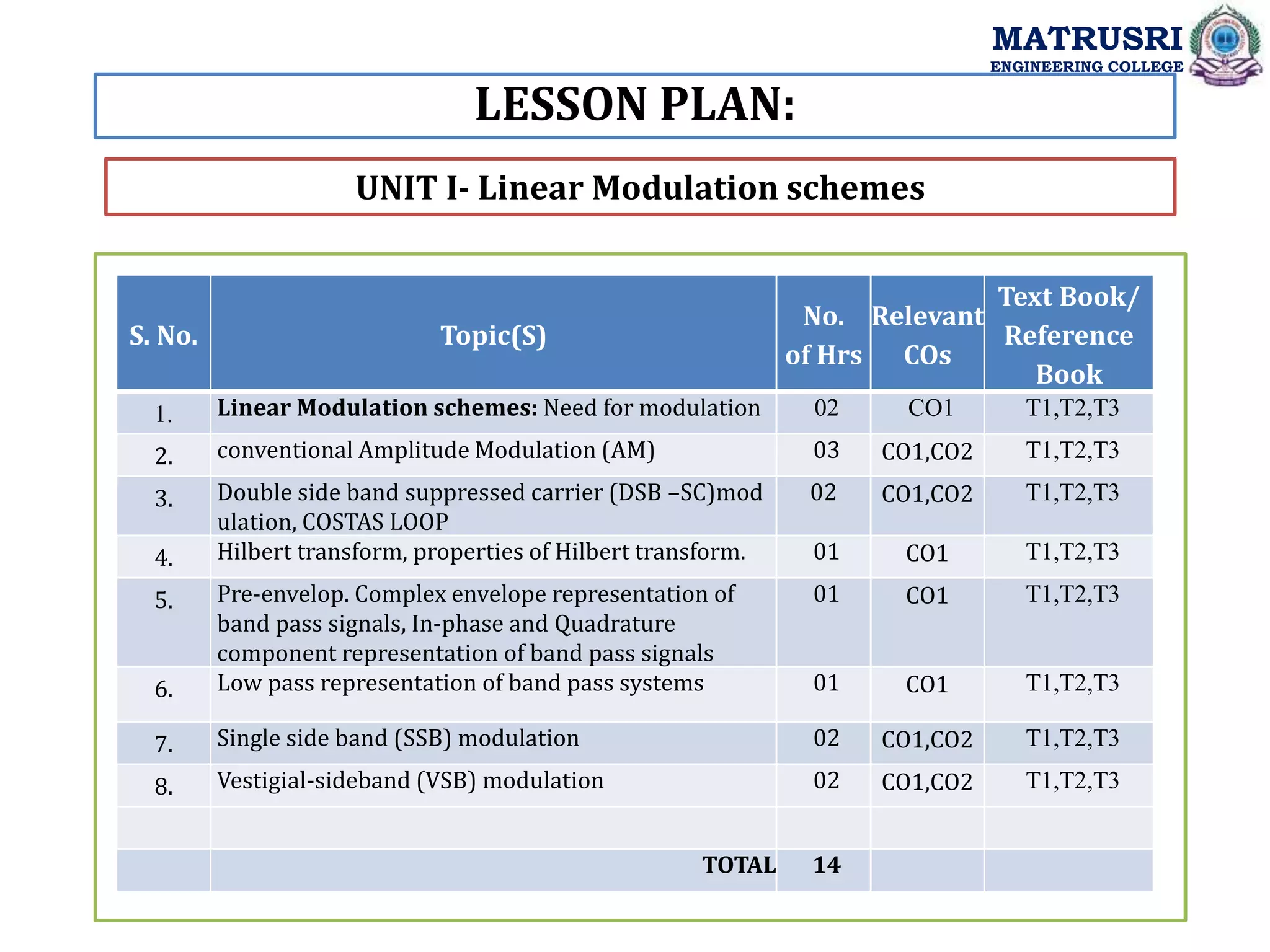
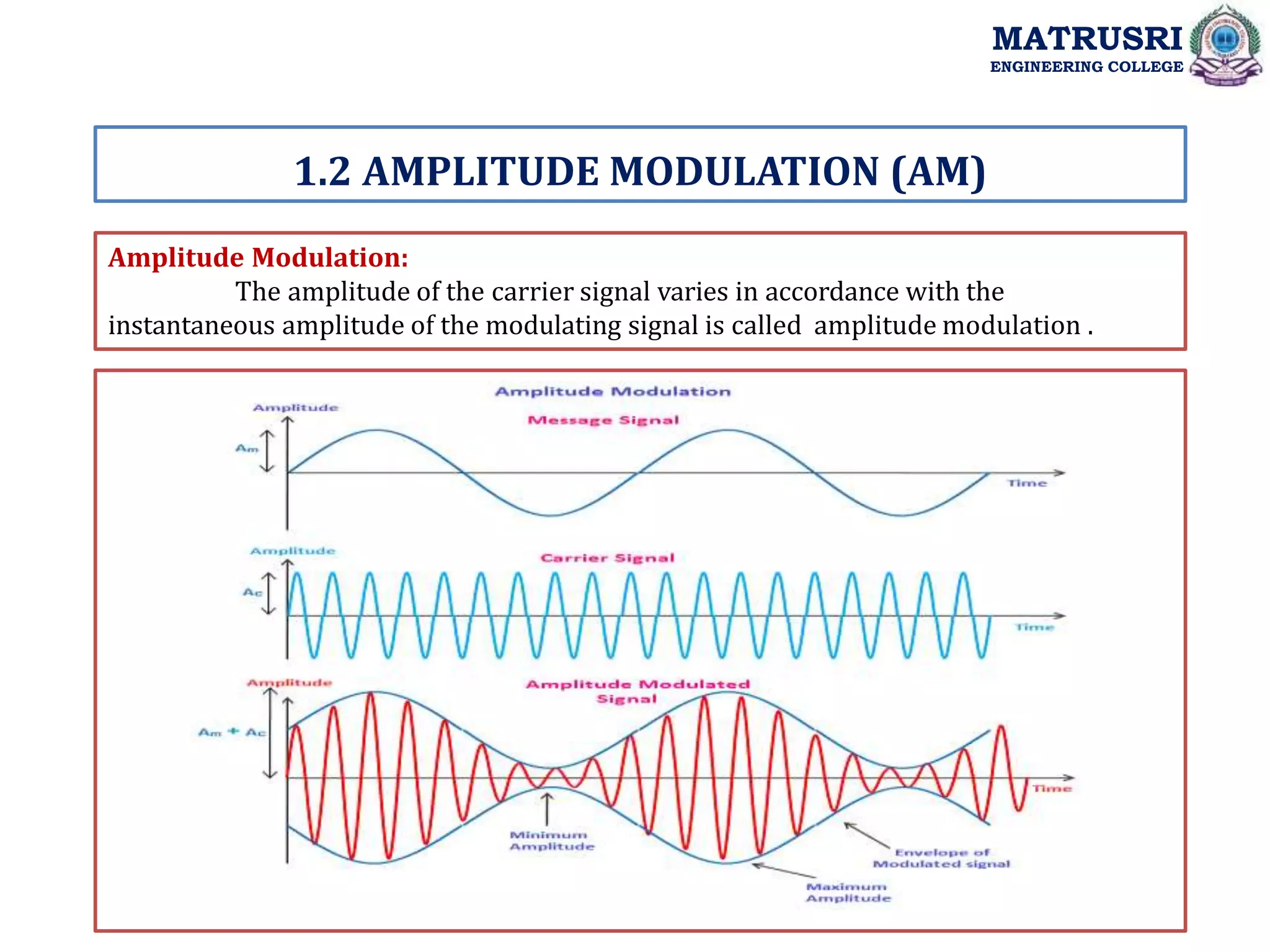
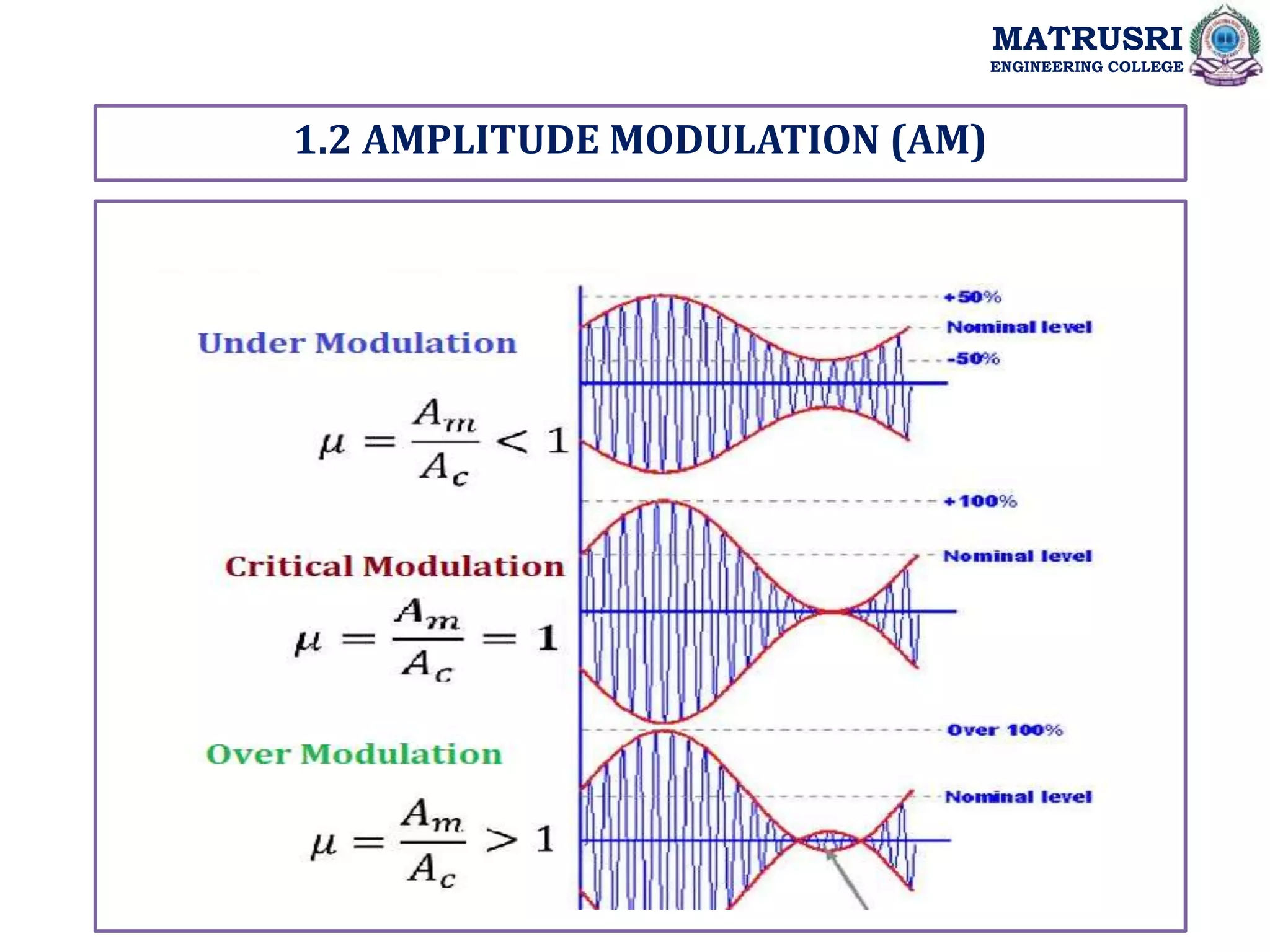
![1.2 AMPLITUDE MODULATION (AM)
MATRUSRI
ENGINEERING COLLEGE
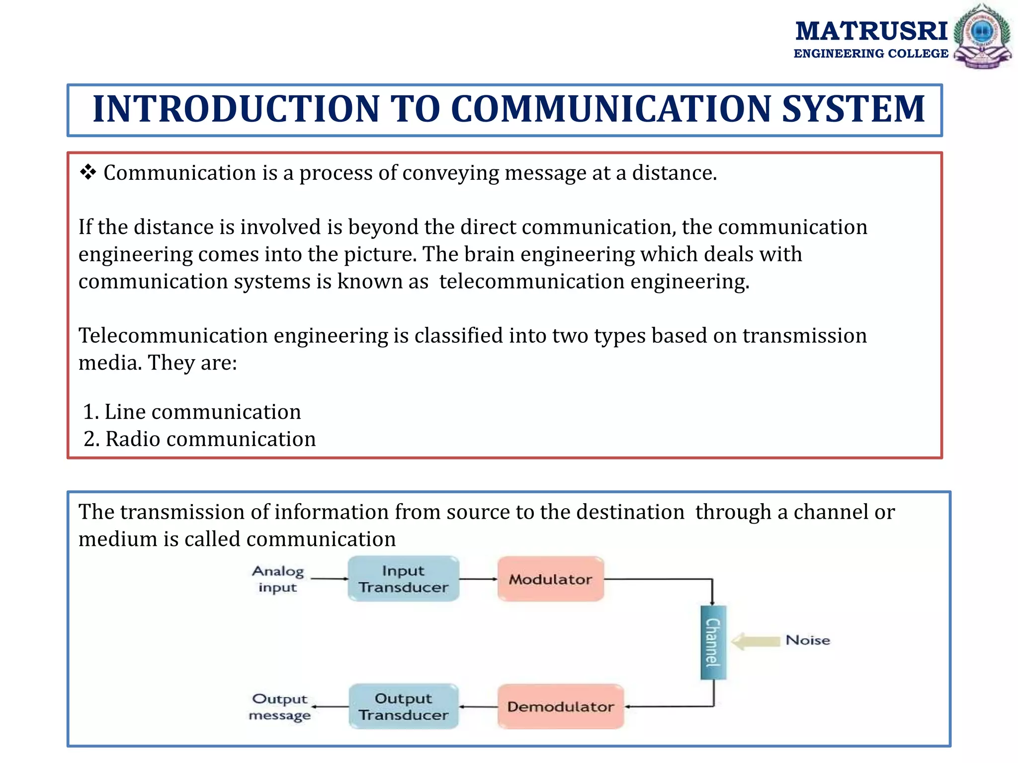
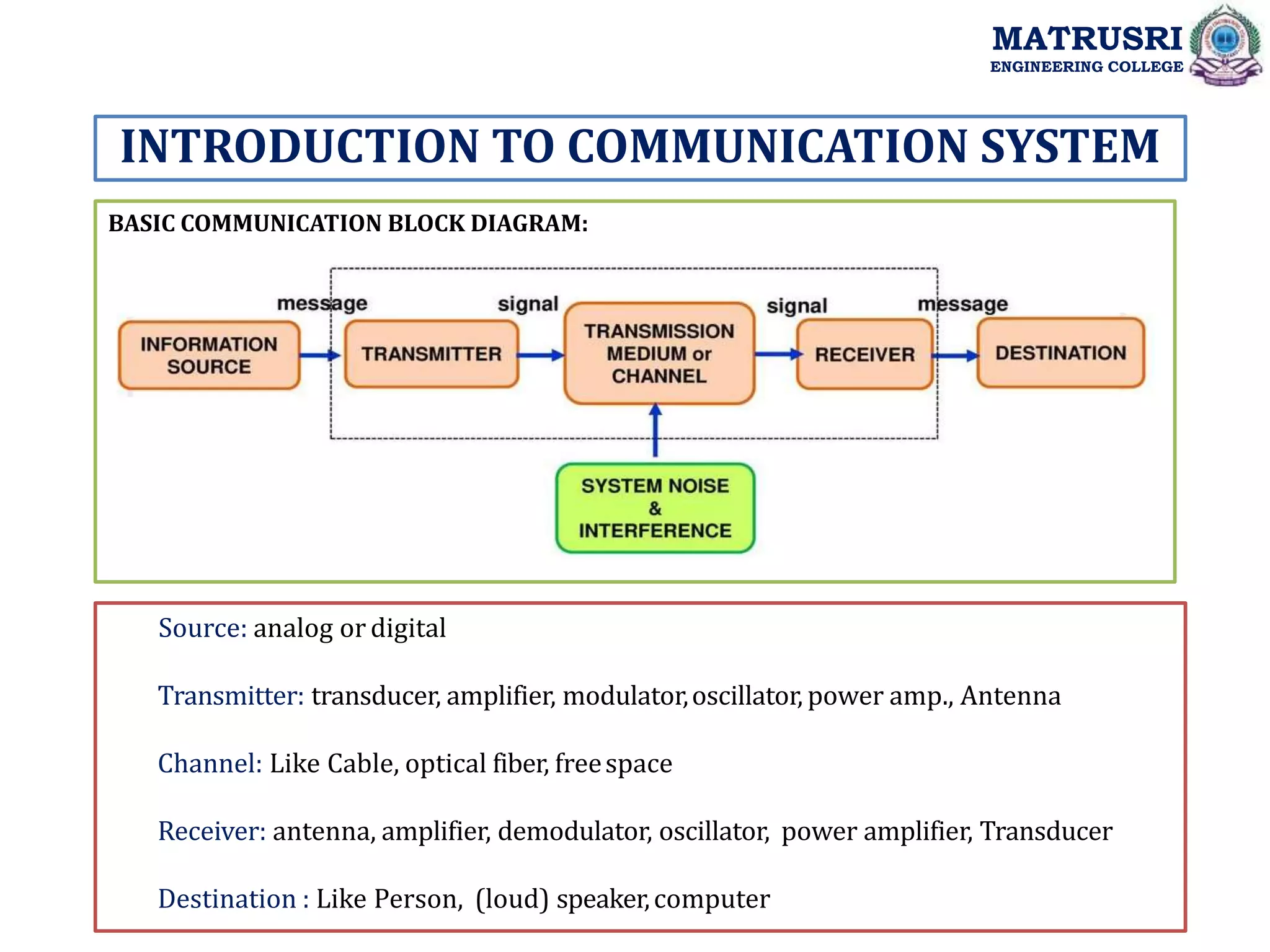
Time-domain Representation of the Waves:
Let the modulating signal be, m(t) = Am cos(2πfmt) eq., 1
and the carrier signal be, c(t)= Ac cos(2πfct) eq.,2
Where,
Am and Ac are the amplitude of the modulating signal and the carrier signal
respectively.
fm and fc are the frequency of the modulating signal and the carrier signal
respectively.
For our convenience, assume the phase angle of the carrier signal is zero. An amplitude-
modulated (AM) wave S(t) can be described as function of time is given by
S (t) = Ac [1+ka m (t)] cos2πfct eq.,3
Where ka = Amplitude sensitivity of the modulator](https://image.slidesharecdn.com/unit-1amplitudemodulation-230123162459-34a0f0b8/75/Unit-1-Amplitude-Modulation-ppt-19-2048.jpg)
![The equation 3, can be written as
S (t) = Ac cos2πfct + Ac ka m (t) cos2πfct eq., 4
The carrier wave, after being modulated, if the modulated level is calculated, then it is
called as Modulation Index or Modulation Depth .
SAM (t) = Ac [1+ka Am cos(2πfmt)] cos2πfct eq., 5
SAM (t) = Ac [1+µcos(2πfmt)] cos2πfct eq.,6
Where µ is “Modulation Index” or “Depth of Modulation”
1.2 AMPLITUDE MODULATION (AM)
MATRUSRI
ENGINEERING COLLEGE
c
m
A
A
2
/
2
/
min
max
min
max
A
A
A
A
A
A
c
m
m
in
m
ax
m
in
m
ax
A
A
A
A
then
eq.,7
eq.,8
eq.,9](https://image.slidesharecdn.com/unit-1amplitudemodulation-230123162459-34a0f0b8/75/Unit-1-Amplitude-Modulation-ppt-20-2048.jpg)
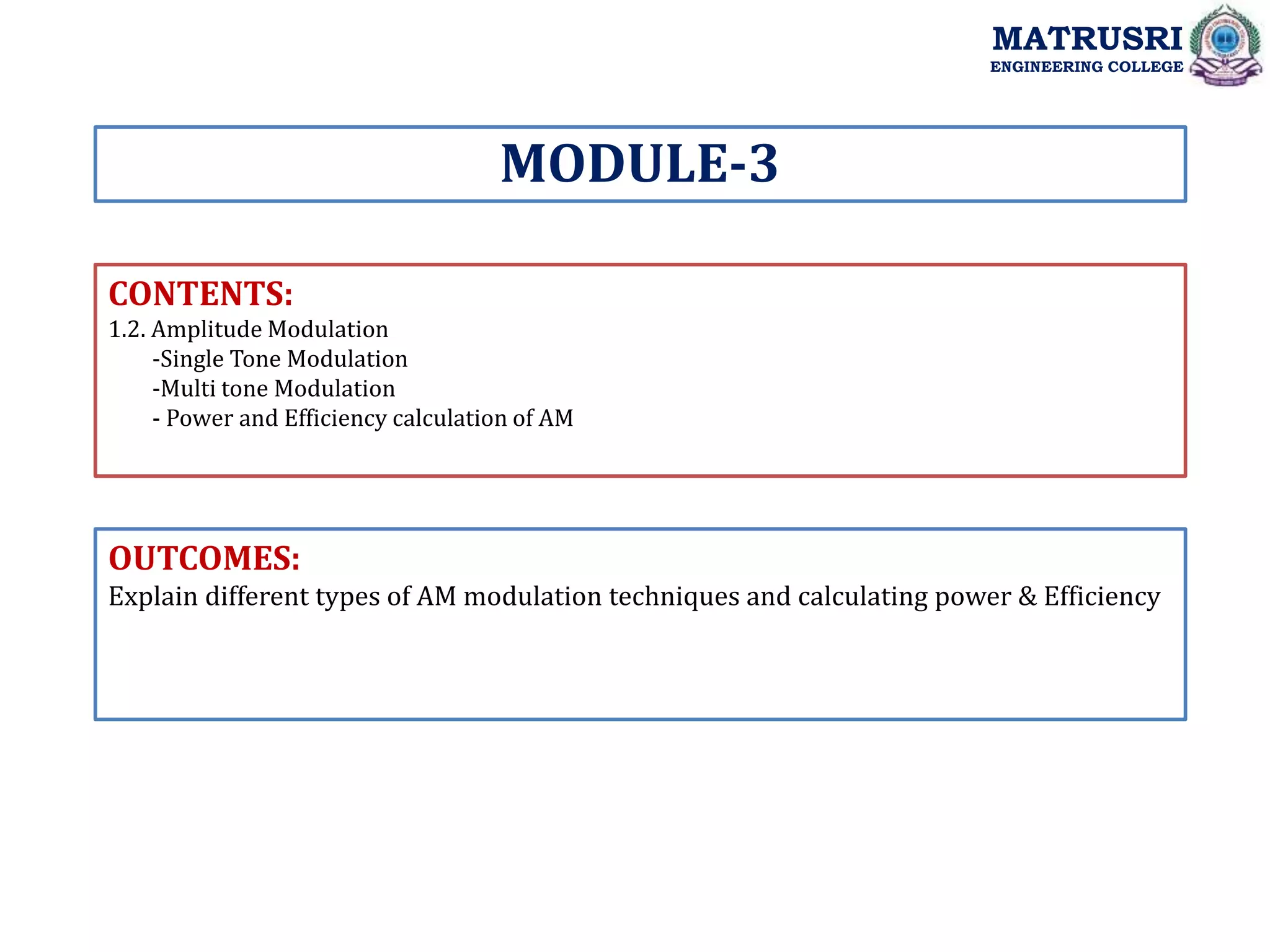
![Single Tone Modulation:
Single tone modulation is “a modulation in which the modulation is carried out by a single frequency
(tone) signal”.
The toned (single frequency) modulating signal consists of only one frequency component and this
signal is modulated with a carrier signal.
Amplitude modulates signal SAM (t) = Ac [1+ka m (t)] cos2πfct
Let us consider single modulating signal m(t) = Am cos(2πfmt)
S (t) = Ac Cos (2π fct)+Acµ /2[cos2 π(fc+fm)t]+ Acµ /2[cos2π (fc-fm)t]
Fourier transform of S (t) is :
S (f) =Ac/2[𝝳 (f-fc) + (f+fc)] +Acµ /4[𝝳 (f-fc-fm) +𝝳 (f+fc+fm)]
+ Acµ /4[𝝳 (f- fc+fm ) +𝝳 (f+fc-fm)]
1.2 AMPLITUDE MODULATION (AM)
MATRUSRI
ENGINEERING COLLEGE
eq.,11
eq.,12](https://image.slidesharecdn.com/unit-1amplitudemodulation-230123162459-34a0f0b8/75/Unit-1-Amplitude-Modulation-ppt-24-2048.jpg)
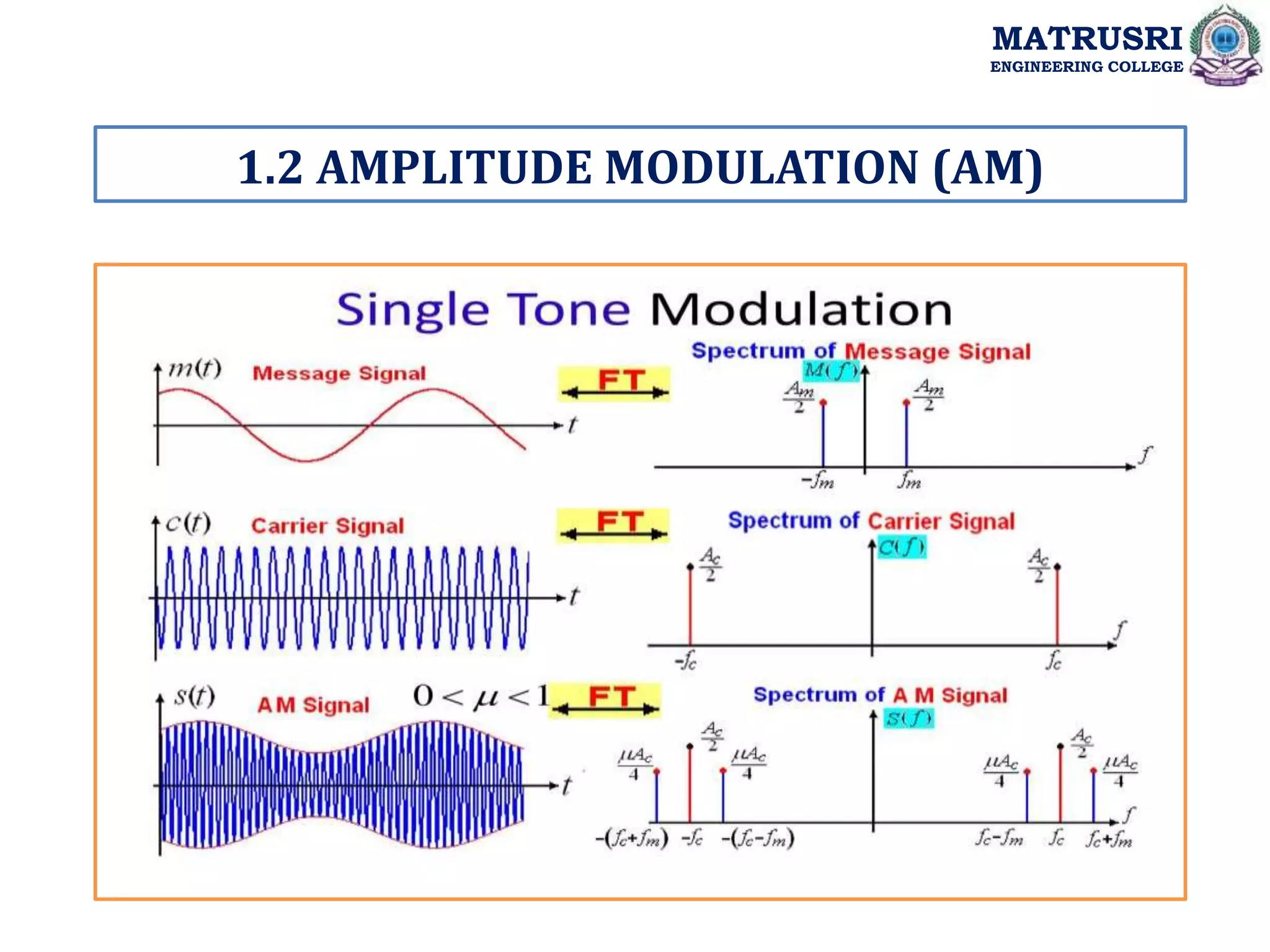
![Multi Tone Modulation:
In multi-tone modulation modulating signal consists of more than one frequency component where
as in single-tone modulation modulating signal consists of only one frequency component .
Amplitude modulates signal SAM (t) = Ac [1+ka m (t)] cos2πfct
Let us consider single modulating signal m(t) = Am1cos(2πfm1t)+ Am2cos(2πfm2t)+-----
S (t) = Ac Cos (2π fct)+Acµ1 /2[cos2 π(fc+fm1)t]+ Acµ1 /2[cos2π (fc-fm1)t]
+Acµ2 /2[cos2 π(fc+fm2t]+ Acµ1 /2[cos2π (fc-fm2)t]+------
Fourier transform of S (t) is :
S (f) =Ac/2[𝝳 (f-fc) + (f+fc)] +Acµ1 /4[𝝳 (f-fc-fm1) +𝝳 (f+fc+fm1)]
+ Acµ1 /4[𝝳 (f- fc+fm1 ) +𝝳 (f+fc-fm1)]
+ Acµ2 /4[𝝳 (f-fc-fm2) +𝝳 (f+fc+fm2)]
+ Acµ2 /4[𝝳 (f- fc+fm2 ) +𝝳 (f+fc-fm2)]+----------
1.2 AMPLITUDE MODULATION (AM)
MATRUSRI
ENGINEERING COLLEGE
eq.,13
eq.,14
eq.,15](https://image.slidesharecdn.com/unit-1amplitudemodulation-230123162459-34a0f0b8/75/Unit-1-Amplitude-Modulation-ppt-26-2048.jpg)
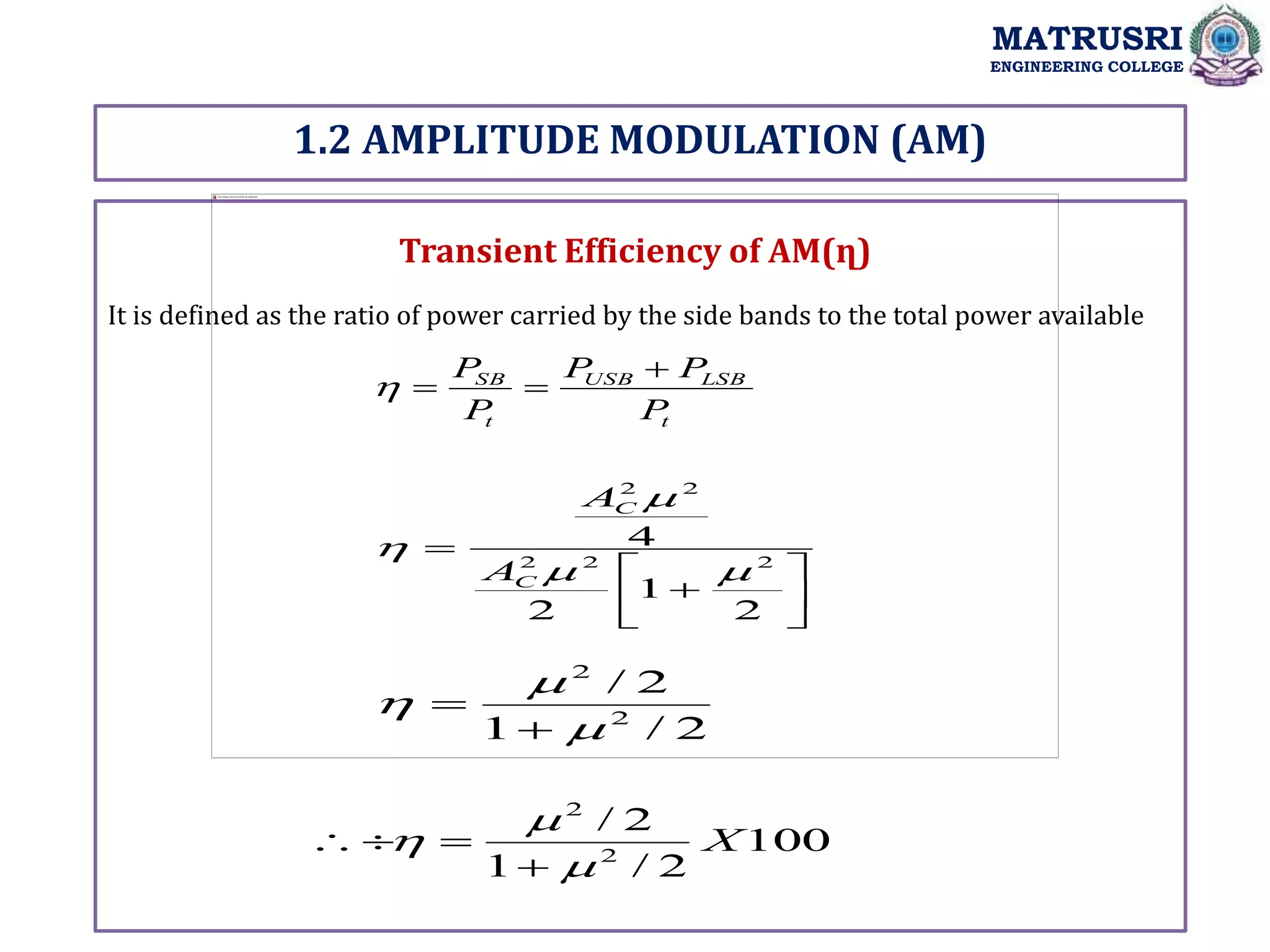
![1.2 AMPLITUDE MODULATION (AM)
MATRUSRI
ENGINEERING COLLEGE
Power Calculation of AM
Single - tone Modulation
Let the modulating signal be, m(t) = Am cos(2πfmt)
and the carrier signal be, c(t)= Ac cos(2πfct)
Then AM equation is S (t) = Ac [1+ka m (t)] cos2πfct
S (t) = Ac Cos (2π fct)+Acµ /2[cos2 π(fc+fm)t]+ Acµ /2[cos2π (fc-fm)t]
Total Power: Pt= Pc + PUSB+PLSB
Power of any signal is equal to the mean square value of the signal
Carrier power Pc = Ac2/2
Upper Side Band power PUSB = Ac2 µ2/8
Lower Side Band power P LSB = Ac2 µ2/8
Total power Pt = Pc + PLSB + PUSB
Total power Pt = Ac2/2 + Ac2 µ2/8 + Ac2 µ2/8
= Ac2/2 + Ac2 µ2/4
= Ac2/2[1 + µ2/2]](https://image.slidesharecdn.com/unit-1amplitudemodulation-230123162459-34a0f0b8/75/Unit-1-Amplitude-Modulation-ppt-28-2048.jpg)
![1.2 AMPLITUDE MODULATION (AM)
MATRUSRI
ENGINEERING COLLEGE
Power Calculation of AM
Total power Pt = Ac2/2 + Ac2 µ2/8 + Ac2 µ2/8
= Ac2/2 + Ac2 µ2/4
= Ac2/2[1 + µ2/2]
Total power Pt =
Total power Pt =
2
2
2
1
2
c
A
2
2
1
c
P
1
2
1
2
1
2
2
c
t
C
T
c
t
I
I
V
V
P
P
](https://image.slidesharecdn.com/unit-1amplitudemodulation-230123162459-34a0f0b8/75/Unit-1-Amplitude-Modulation-ppt-29-2048.jpg)
![1.2 AMPLITUDE MODULATION (AM)
MATRUSRI
ENGINEERING COLLEGE
Power Calculation of AM
Multi-tone Modulation:
Total Power: Pt= Pc + PUSB1+PLSB1 + PUSB2+PLSB2+-------------------
Total power Pt = Ac2/2 + Ac2 µ12/8 + Ac2 µ12/8 + Ac2 µ22/8 + Ac2 µ22/8+--------
= Ac2/2 + Ac2 µ12/4 + Ac2 µ22/4+---------
= Ac2/2[1 + µ12/2+ µ22/2+-----]
= Ac2/2[1 + µt2/2]
Total power Pt = Pc[1 + µt2/2]](https://image.slidesharecdn.com/unit-1amplitudemodulation-230123162459-34a0f0b8/75/Unit-1-Amplitude-Modulation-ppt-31-2048.jpg)
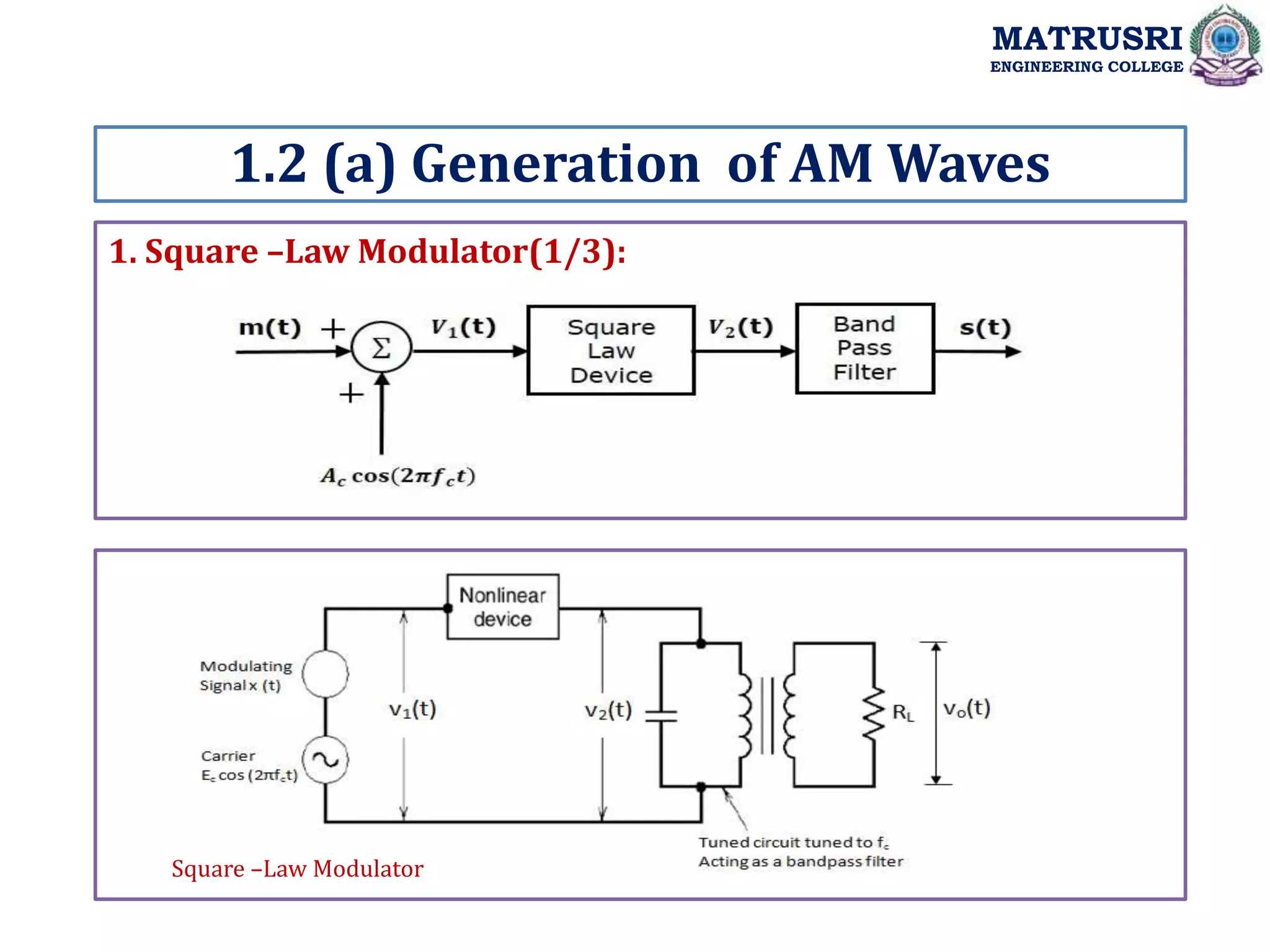
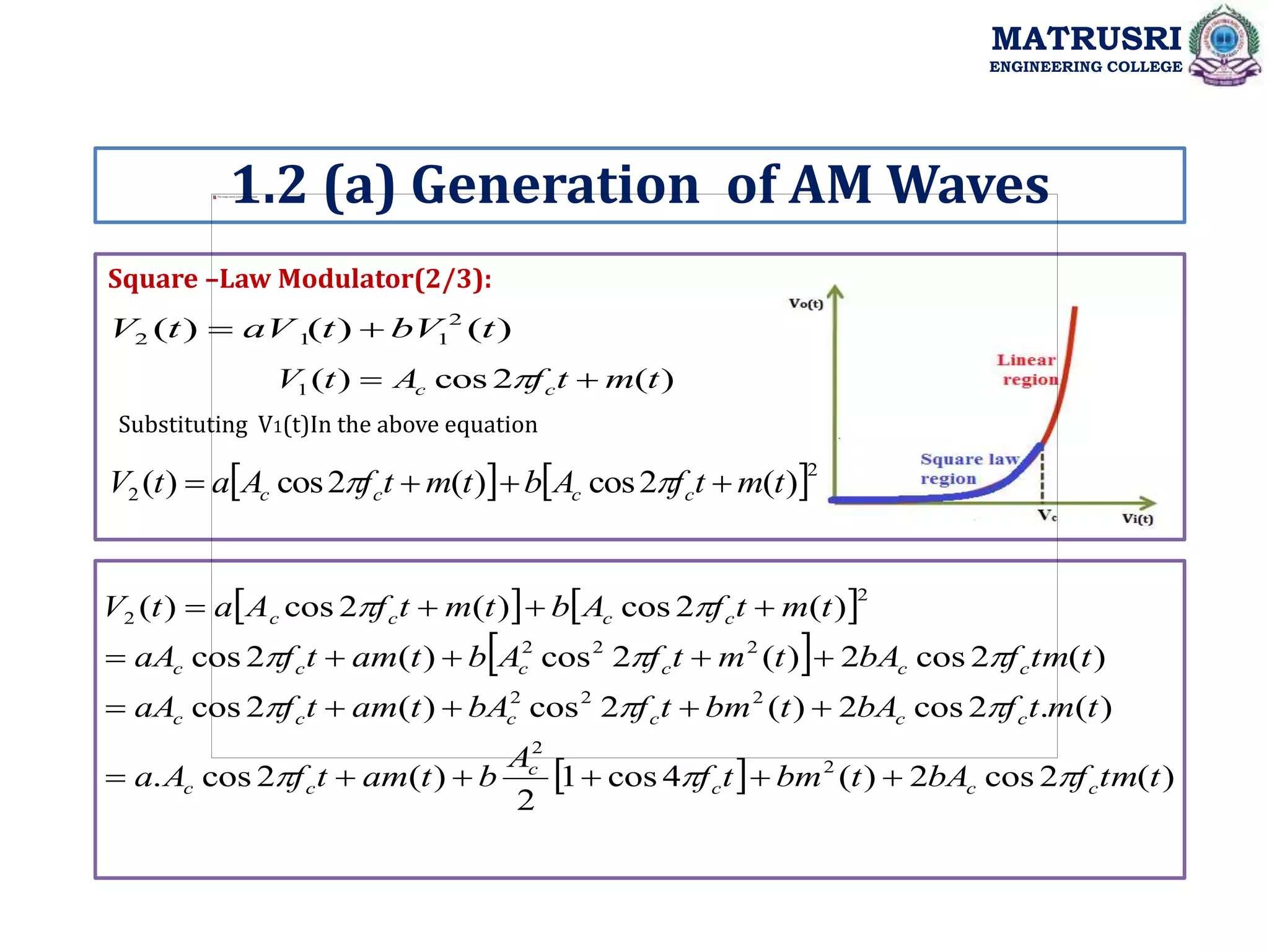
![Square –Law Modulator(3/3):
Applying Fourier transform:
MATRUSRI
ENGINEERING COLLEGE
1.2 (a) Generation of AM Waves
After Passing through a BPF with the cutoff frequency fc
t
f
t
m
a
b
aA
t
bm
a
t
f
A
t
m
t
f
bA
t
f
aA
t
V
c
c
c
c
c
c
c
c
2
cos
)
(
2
1
)
(
2
2
cos
)
(
.
2
cos
2
2
cos
)
(
2
)]
(
)
(
[
2
)]
2
(
)
2
(
[
4
)
(
2
)
(
)
(
2
)
(
)
(
2
)
(
)
(
2
2
4
2
c
c
c
c
c
c
c
c
c
c
f
f
M
f
f
M
bA
f
f
f
f
bA
f
bA
f
M
f
M
b
f
f
f
f
A
a
f
aM
f
V
](https://image.slidesharecdn.com/unit-1amplitudemodulation-230123162459-34a0f0b8/75/Unit-1-Amplitude-Modulation-ppt-37-2048.jpg)
![2. Switching Modulator :
1.2 (a) Generation of AM Waves
MATRUSRI
ENGINEERING COLLEGE
)
(
2
cos
)
(
2 t
m
t
f
A
t
V c
c
0
)
(
)
( 2
1
t
V
t
V C(t) > 0
C(t) <0
)
(
).
(
)
( 1
2 t
g
t
V
t
V p
Mathematically
With period To=1/fc and a duty cycle of 50%
)]
2
2
(
2
cos[
1
2
1
2
2
1
)
(
1
1
n
t
f
n
t
g c
n
n
p
](https://image.slidesharecdn.com/unit-1amplitudemodulation-230123162459-34a0f0b8/75/Unit-1-Amplitude-Modulation-ppt-38-2048.jpg)
![2. Switching Modulator :
1.2 (a) Generation of AM Waves
MATRUSRI
ENGINEERING COLLEGE
cs
oddHarmoni
t
f
t
g c
p
2
cos
2
2
1
)
(
]
2
cos
2
2
1
)][
(
2
cos
[
)
( cs
oddHarmoni
t
f
t
m
t
f
A
t
g c
c
c
p
cs
oddHarmoni
f
A
A
t
f
A
t
f
t
m
t
m
t
V
c
c
c
c
c
c
4
cos
2
cos
2
2
cos
)
(
2
2
)
(
)
(
2
t
f
A
t
f
t
m
t
V c
c
c
2
cos
2
2
cos
)
(
2
)
(
2
)]
(
1
[
2
cos
2
t
m
A
a
t
f
A
c
c
c
After Passing through a BPF](https://image.slidesharecdn.com/unit-1amplitudemodulation-230123162459-34a0f0b8/75/Unit-1-Amplitude-Modulation-ppt-39-2048.jpg)
![1. Synchronous/Coherent Detector(1/2):
1.2 (b) Detection of AM Waves
MATRUSRI
ENGINEERING COLLEGE
t
f
A
t
f
t
m
k
A
t
S c
c
c
a
c
AM
2
cos
.
2
cos
)]
(
1
[
)
(
t
f
t
m
k
A
t
m
k
A
t
f
A
A
t
S c
a
c
a
c
c
c
c
AM )
2
(
2
cos
)
(
2
)
(
2
)
2
(
2
cos
2
2
)
(
2
2
2
2
)
(
2
)
(
2
t
m
k
A
t
S a
c
AM After Passing through LPF](https://image.slidesharecdn.com/unit-1amplitudemodulation-230123162459-34a0f0b8/75/Unit-1-Amplitude-Modulation-ppt-41-2048.jpg)
![1. Synchronous/Coherent Detector(2/2):
1.2 (b) Detection of AM Waves
MATRUSRI
ENGINEERING COLLEGE
t
f
A
t
f
t
m
k
A
t
S c
c
c
a
c
AM )
2
cos(
.
2
cos
)]
(
1
[
)
(
t
t
f
t
t
f
A
t
f
t
m
k
A
A
t
S c
c
c
c
a
c
c
AM )
sin(
.
2
sin
cos
)
2
[cos(
.
2
cos
)]
(
[
)
(
For a phase ø:
When there is no proper synchronization ,then
cos
).
(
2
)
(
2
t
m
k
A
t
V a
c
o
)
(
2
)
(
2
t
m
k
A
t
V a
c
o
then
o
If ,
0
0
;
,
90 0
0
V
then
If
i.e., There is no De-Modulated output. This effect is called “ Quadrature -Null effect” .
In order to avoid above problem, we will maintain synchronization at receiver , but the
complexity of receiver will increase.](https://image.slidesharecdn.com/unit-1amplitudemodulation-230123162459-34a0f0b8/75/Unit-1-Amplitude-Modulation-ppt-42-2048.jpg)
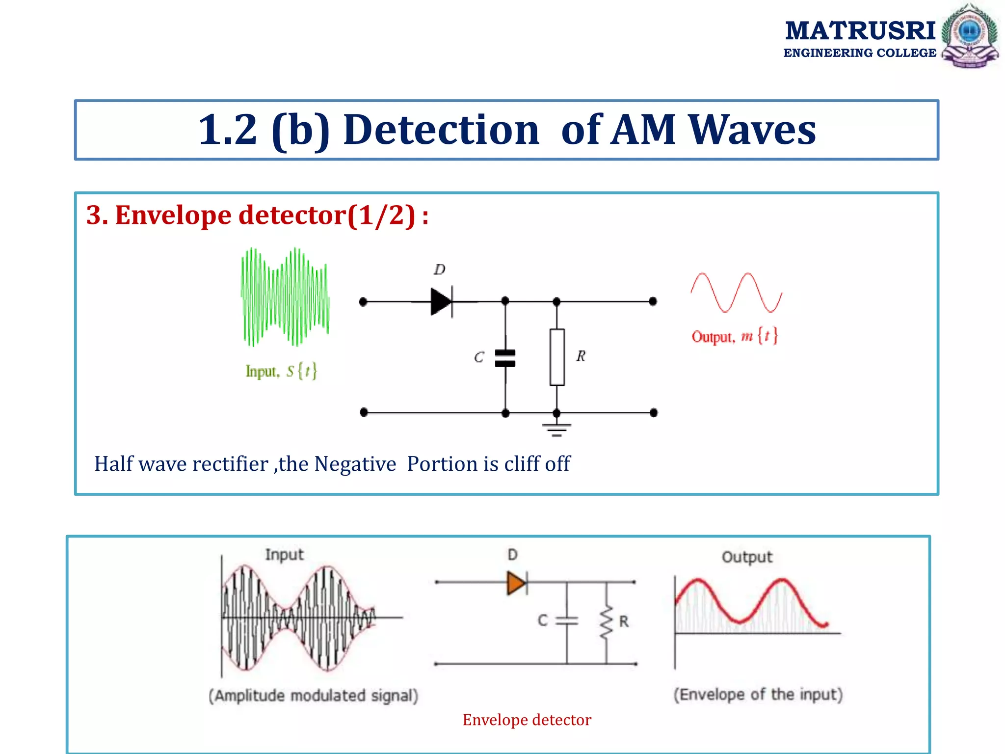
![2.SQUARE-LAW DETECTOR(1/2) :
1.2 (b) Detection of AM Waves
MATRUSRI
ENGINEERING COLLEGE
)
(
)
(
)
( 2
1
1
2 t
bV
t
aV
t
V
]
2
cos
)
(
1
(
[
]
2
cos
)
(
1
(
[
)
(
2
cos
)]
(
1
[
)
(
2
2
2
2
1
t
f
t
m
k
A
b
t
f
t
m
k
A
a
t
V
t
f
t
m
k
A
t
V
c
a
c
c
a
c
c
a
c
]
2
/
)
2
(
2
cos
1
)]
(
2
)
(
1
(
[
2
cos
)
(
2
cos
)
( 2
2
2
2 t
f
t
m
k
t
m
k
A
b
t
f
t
m
k
aA
t
f
aA
t
V c
a
a
c
c
a
c
c
c
]
)
2
(
2
cos
1
)][
(
2
2
)
(
2
2
[
2
cos
)
(
2
cos
2
2
2
2
2
2
2
t
f
t
m
k
A
b
t
m
k
bA
bA
t
f
t
m
k
aA
t
f
aA
c
a
c
a
c
c
c
a
c
c
c
](https://image.slidesharecdn.com/unit-1amplitudemodulation-230123162459-34a0f0b8/75/Unit-1-Amplitude-Modulation-ppt-43-2048.jpg)
![2.SQUARE-LAW DETECTOR(2/2) :
After passing through the LPF:
1.2 (b) Detection of AM Waves
MATRUSRI
ENGINEERING COLLEGE
)
(
)
(
2
2
)
(
]
)
2
(
2
cos
)]
(
)
(
2
2
[
)]
(
)
(
2
2
[
2
cos
)
(
2
cos
)
(
2
2
2
2
2
2
2
2
2
2
2
2
2
2
2
2
t
m
k
bA
t
m
k
bA
bA
t
y
t
f
t
m
k
bA
t
m
k
bA
bA
t
m
k
bA
t
m
k
bA
bA
t
f
t
m
k
aA
t
f
aA
t
V
a
c
a
c
c
c
a
c
a
c
c
a
c
a
c
c
c
a
c
c
c
)
(
)
(
2
)
( 2
2
2
2
2
t
m
k
bA
t
m
k
bA
t
V a
c
a
c
o
The unwanted terms gives rise to signal
distortion . The ratio to the desired signal
to undesired signal
)
(
2
)
(
2
)
(
2
2
2
2
t
m
k
t
m
k
bA
t
m
k
bA
N
S
a
a
c
a
c
](https://image.slidesharecdn.com/unit-1amplitudemodulation-230123162459-34a0f0b8/75/Unit-1-Amplitude-Modulation-ppt-44-2048.jpg)
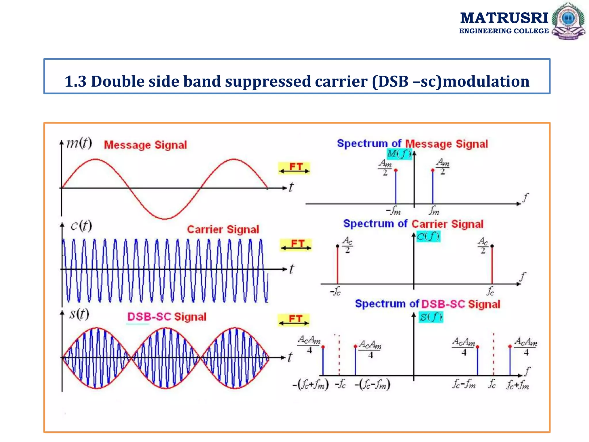
![Single-Tone Modulation
DSB-SC Modulated signal is: S (t) = Ac ka cos2πfct. m (t)
For a single tone ,
m(t)= Am cos2πfmt
Then, S (t) = Ac ka cos2πfct. Am cos2πfmt
= Ac Am/2[cos2π(fc + fm)t +cos2π(fc - fm)t ]
Fourier transform of S (t) is :
S (f) =AcAm /4[𝝳 (f-fc-fm) +𝝳 (f+fc+fm)] + AcAm /4[𝝳 (f- fc+fm ) +𝝳 (f+fc-fm)]
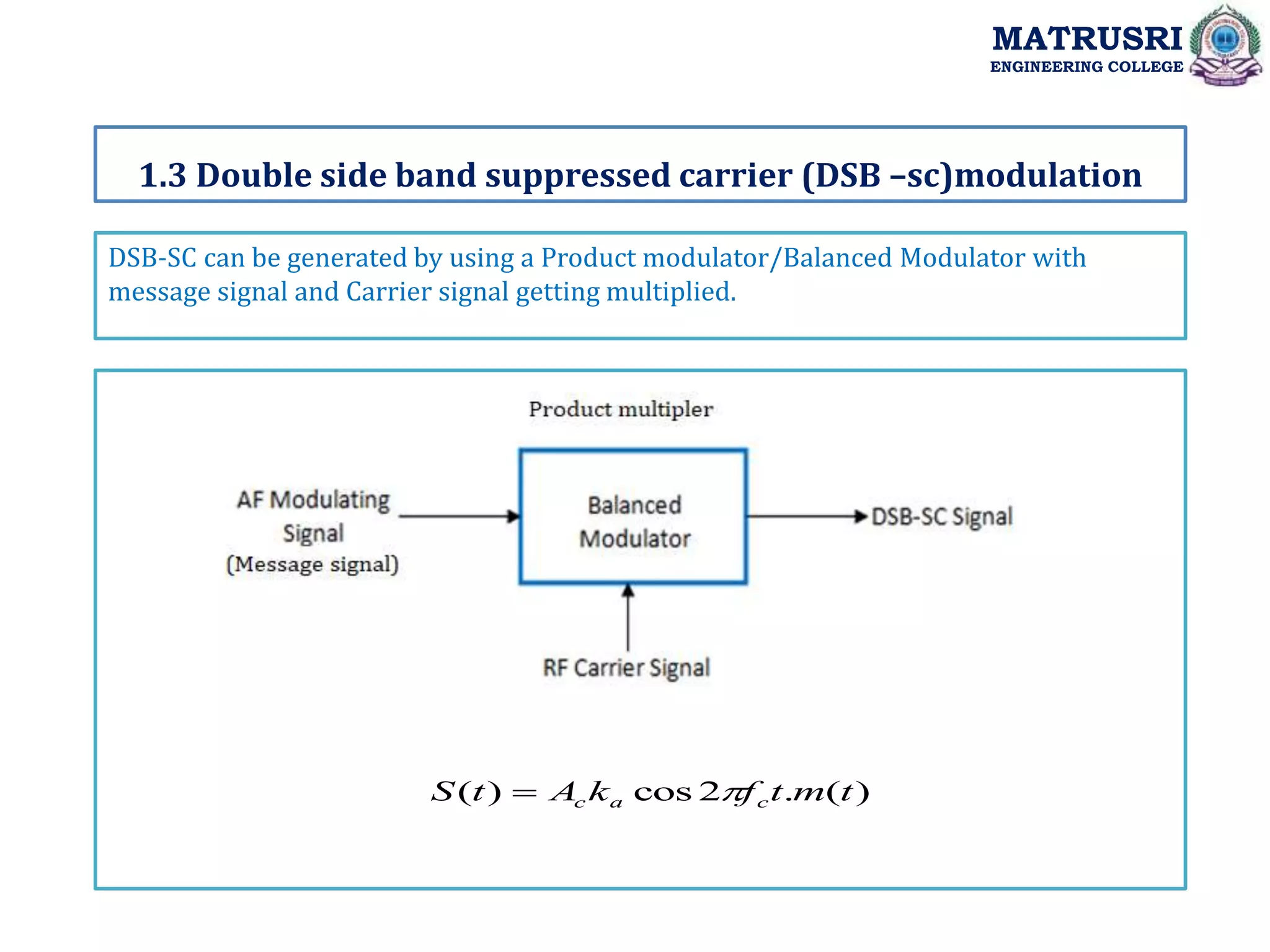
1.3 Double side band suppressed carrier (DSB –sc)modulation
MATRUSRI
ENGINEERING COLLEGE](https://image.slidesharecdn.com/unit-1amplitudemodulation-230123162459-34a0f0b8/75/Unit-1-Amplitude-Modulation-ppt-52-2048.jpg)
![1.3 DOUBLE SIDE BAND SUPPRESSED CARRIER (DSB –SC)MODULATION
MATRUSRI
ENGINEERING COLLEGE
Power Calculation of DSB-SC
Let the modulating signal be, m(t) = Am cos (2πfmt)
and the carrier signal be, c(t)= Ac cos (2πfct)
Then DSB-SC equation is S (t) = Ac ka cos2πfct. m (t)
S (t) = Ac Am/2[cos2π(fc + fm)t +cos2π(fc - fm)t ]
Total Power: Pt= PUSB+PLSB
Total power Pt = Ac2 µ2/8 + Ac2 µ2/8
= Ac2 µ2/4
= Pc . µ2/2
Efficiency:
t
LSB
USB
t
SB
P
P
P
P
P
Efficiency is 100%](https://image.slidesharecdn.com/unit-1amplitudemodulation-230123162459-34a0f0b8/75/Unit-1-Amplitude-Modulation-ppt-54-2048.jpg)
![1.3.(A) Generation of DSB-SC Waves
.
MATRUSRI
ENGINEERING COLLEGE
t
f
t
m
k
A
t
x c
a
c
2
cos
)]
(
1
[
)
(
1
The output of First AM generator is
The output of Second AM generator is t
f
t
m
k
A
t
x c
a
c
2
cos
)]
(
1
[
)
(
2
The output of Summer is: x1-x2:
t
f
t
m
k
A
t
f
t
m
k
A
t
y c
a
c
c
a
c
2
cos
)]
(
1
[
2
cos
)]
(
1
[
)
(
2
1
2
2
1
2
1 4
2 V
V
a
V
a
id
id
i
C
c
a A
t
f
t
m
k
t
y .
2
cos
).
(
2
)
(
](https://image.slidesharecdn.com/unit-1amplitudemodulation-230123162459-34a0f0b8/75/Unit-1-Amplitude-Modulation-ppt-58-2048.jpg)
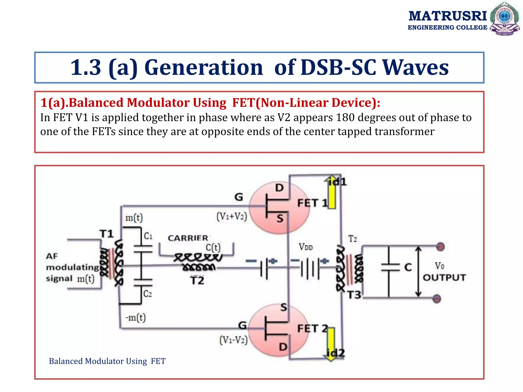
![1(a).Balanced Modulator Using FET(Non-Linear Device):
The currents output of push-pull center taped transformer id1:
1.3 (a) Generation of DSB-SC Waves
MATRUSRI
ENGINEERING COLLEGE
2
2
1
2
2
1
1
0
1 )
(
)
( V
V
a
V
V
a
a
id
2
2
1
2
2
1
1
0
2 )
(
)
( V
V
a
V
V
a
a
id
Then the output is:
2
1
2
2
1
2
1 4
2 V
V
a
V
a
id
id
i
If the output tank circuit tuned to a center frequency fc, then V0α I
)
(
2
cos
]
4
[
2
1
2
1
2
0
t
m
V
t
f
A
V
V
V
a
k
kI
V
c
c
ka
wherek
t
f
t
m
A
k
t
m
t
f
A
a
k
V
c
c
c
c
4
2
cos
).
(
.
.
)]
(
.
2
cos
.
4
[
1
1
2
0
Then](https://image.slidesharecdn.com/unit-1amplitudemodulation-230123162459-34a0f0b8/75/Unit-1-Amplitude-Modulation-ppt-60-2048.jpg)
![1.3 (a) Generation of DSB-SC Waves
MATRUSRI
ENGINEERING COLLEGE
2. Ring Modulator(1/2):
Mathematically the square wave is represented as:
]
)
1
2
(
2
cos[
1
2
)
1
(
4
)
( 1
1
t
n
f
n
t
c c
n
n
.....]
)
3
(
2
cos
3
1
2
[cos
4
)
(
t
f
t
f
t
c c
c
](https://image.slidesharecdn.com/unit-1amplitudemodulation-230123162459-34a0f0b8/75/Unit-1-Amplitude-Modulation-ppt-62-2048.jpg)
![2. RING MODULATOR(2/2):
The output of the Ring Modulator is :
When s(t) is passed through a BPF, Then the o/p of the filter is:
1.3 (a) Generation of DSB-SC Waves
MATRUSRI
ENGINEERING COLLEGE
.....)]
)
3
(
2
cos
).
(
3
1
2
cos
).
(
[
4
)
(
.....)]
)
3
(
2
cos
3
1
2
[cos
4
)(
(
)
(
)
(
).
(
)
(
t
f
t
m
t
f
t
m
t
s
t
f
t
f
t
m
t
s
t
c
t
m
t
s
c
c
c
c
t
f
t
m
t
s c
2
cos
).
(
4
)
( ](https://image.slidesharecdn.com/unit-1amplitudemodulation-230123162459-34a0f0b8/75/Unit-1-Amplitude-Modulation-ppt-63-2048.jpg)
![1.Coherent/Synchronous Detector:
MATRUSRI
ENGINEERING COLLEGE
1.3.(B) Detection of DSB-SC Waves
)
(
2
)
(
]
)
2
(
2
cos
1
)[
(
2
)
(
2
cos
).
(
)
(
2
cos
.
2
cos
).
(
)
(
)
(
2
cos
).
(
)
(
2
2
2
2
t
m
A
t
y
AfterLPF
t
f
t
m
A
t
y
t
f
t
m
A
t
y
t
f
A
t
f
t
m
A
t
y
AfterLPF
t
y
t
f
A
t
S
t
x
c
c
c
c
c
c
c
c
C
c
c
](https://image.slidesharecdn.com/unit-1amplitudemodulation-230123162459-34a0f0b8/75/Unit-1-Amplitude-Modulation-ppt-66-2048.jpg)
![When there is NO Perfect Synchronization, two distortions arises:
1. Effect of Phase distortion
2. Effect of Frequency distortion
1.3(B) Detection of DSB-SC Waves
MATRUSRI
ENGINEERING COLLEGE
0
)
(
,
90
)
(
2
)
(
,
0
cos
)
(
2
)
(
]
cos
)
4
)[cos(
(
2
)
(
)
2
cos(
.
2
cos
)
(
)
(
)
2
cos(
).
(
)
(
0
2
0
2
2
t
y
t
m
A
t
y
when
t
t
m
A
t
y
AfterLPF
t
t
t
f
t
m
A
t
x
t
f
A
t
f
t
m
A
t
x
t
f
A
t
S
t
x
c
c
c
c
c
c
c
c
c
c
1. Effect of Phase distortion:
When there is phase shift of π/2, the demodulated output is zero, Even though the input is
present. This effect is called “Quadrature null effect”](https://image.slidesharecdn.com/unit-1amplitudemodulation-230123162459-34a0f0b8/75/Unit-1-Amplitude-Modulation-ppt-67-2048.jpg)
![2.Effect of Frequency distortion
1.3(B) Detection of DSB-SC Waves
MATRUSRI
ENGINEERING COLLEGE
When there is frequency distortion, each signal undergo a shift of ⍙f and power reduced
By Factor 2. Phase distortion can be tolerated but nor frequency distortion
]
)
2
cos(
)
4
)[cos(
(
2
)
(
)
(
2
cos
.
2
cos
)
(
)
(
)
(
2
cos
).
(
)
(
2
t
f
t
f
f
t
m
A
t
x
f
f
A
t
f
t
m
A
t
x
t
f
f
A
t
S
t
x
c
c
c
c
c
c
c
c
)
2
(
4
2
2
4
)]
(
)
(
[
4
)
(
]
)
(
2
)[cos
(
2
)
(
:
4
4
1
2
2
edby
powerreduc
P
X
A
P
X
A
P
f
f
M
f
f
M
A
F
Y
t
f
t
m
A
t
y
AfterLPF
m
c
m
c
c
c
](https://image.slidesharecdn.com/unit-1amplitudemodulation-230123162459-34a0f0b8/75/Unit-1-Amplitude-Modulation-ppt-68-2048.jpg)
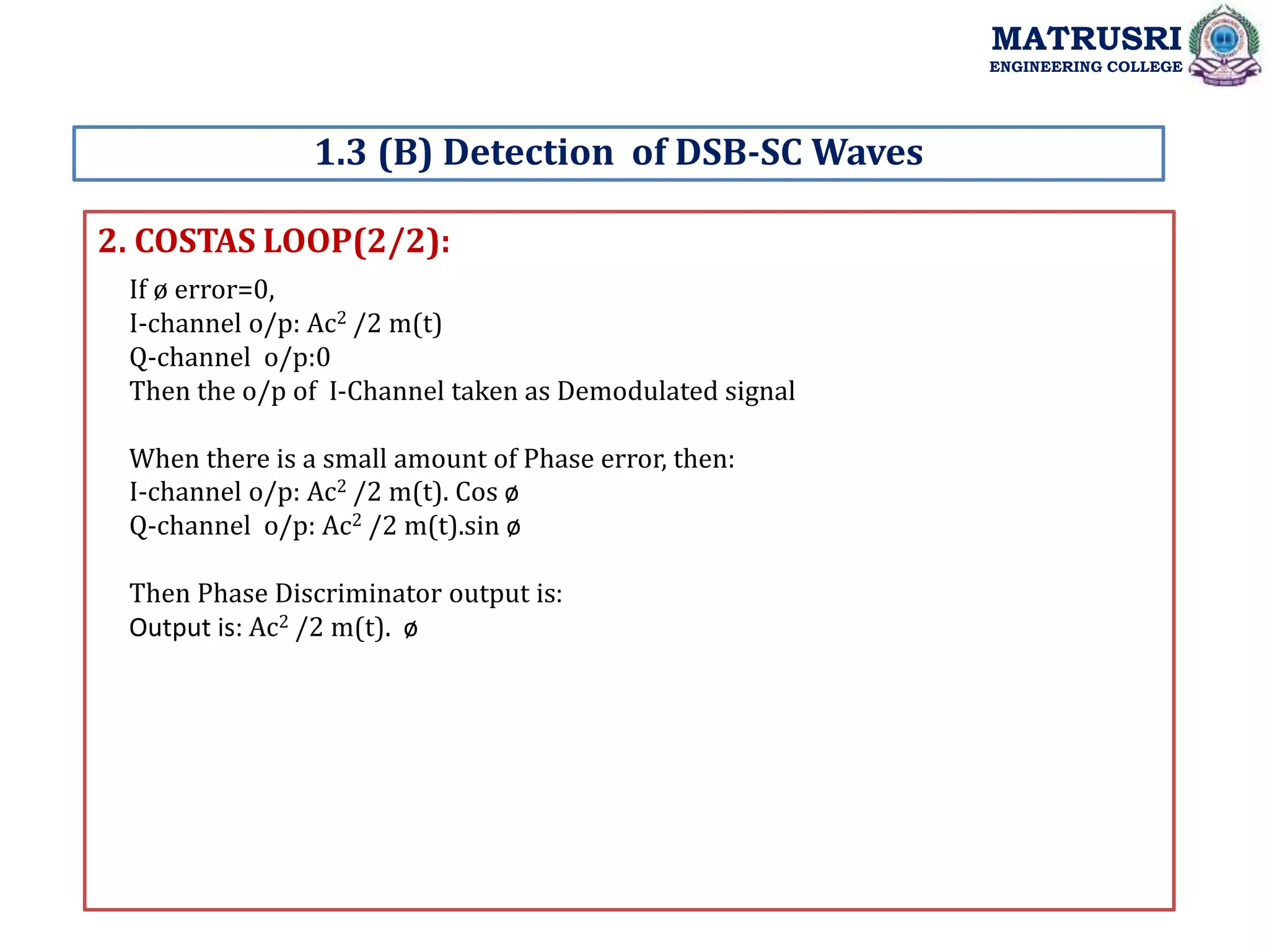
![3. Squaring LOOP:
The limiter output is:
1.3 (B) Detection of DSB-SC Waves
MATRUSRI
ENGINEERING COLLEGE
)
(
.
2
1
4
cos
).
(
2
2
1
)
(
]
4
cos
1
)[
(
2
)
(
)
(
.
2
cos
)
(
)
(
)
(
.
2
cos
.
)
(
2
2
2
2
2
t
m
A
t
f
t
m
A
t
z
t
f
t
m
A
t
y
t
m
t
f
A
t
x
t
y
t
m
t
f
A
t
x
c
c
c
c
c
c
c
c
c
t
f
K
t
w c
4
cos
.
)
( 1
The frequency divider output is:
t
f
K
t
f
K
t
V c
c
2
cos
.
2
4
cos
.
)
( 2
2
](https://image.slidesharecdn.com/unit-1amplitudemodulation-230123162459-34a0f0b8/75/Unit-1-Amplitude-Modulation-ppt-72-2048.jpg)
![Properties of hilbert -transform:
2. Sign reversal:
Applying the hilbert-transform operation to a signal twice causes a sign reversal of the
signal, i.e
X( f ) does not contain any impulses at the origin
1.4 Hilbert transform, properties of Hilbert transform
MATRUSRI
ENGINEERING COLLEGE
)
(
)
(
ˆ
ˆ t
x
t
x
)
(
)
sgn(
)]
(
ˆ
ˆ
[
2
f
X
f
j
t
x
F
)
(
)]
(
ˆ
ˆ
[ f
X
t
x
F
Proof:](https://image.slidesharecdn.com/unit-1amplitudemodulation-230123162459-34a0f0b8/75/Unit-1-Amplitude-Modulation-ppt-77-2048.jpg)
![Properties of hilbert -transform:
4. Orthogonality
The signal x(t) and its hilbert transform are orthogonal
Using Parseval's theorem of the Fourier transform, we obtain
1.4 Hilbert transform, properties of Hilbert transform
MATRUSRI
ENGINEERING COLLEGE
Proof:
df
f
X
f
j
f
X
dt
t
x
t
x *
*
)]
(
)
sgn(
)[
(
)
(
ˆ
)
(
0
)
(
)
(
0
2
0 2
df
f
X
j
df
f
X
j
In the last step, we have used the fact that X(f) is Hermitian;
| X(f)|2 is even.](https://image.slidesharecdn.com/unit-1amplitudemodulation-230123162459-34a0f0b8/75/Unit-1-Amplitude-Modulation-ppt-79-2048.jpg)
![Let x(t) is real valued signal, then complex signal representation is
1.5 .Pre-envelop, complex envelope representation of band pass signals
MATRUSRI
ENGINEERING COLLEGE
Let x(t) be a BP signal(it consists of non –zero freq. components, centered at fc
and BW=2w)
)
(
)
(
)
(
)
(
)
(
)
(
)
(
)
(
)
(
f
jx
f
x
f
x
simillarly
f
jx
f
x
f
x
afterFT
t
jx
t
x
t
x
sin
).
(
.
cos
).
(
]
sin
).[cos
(
).
(
)
(
:
~
t
m
j
t
m
j
t
m
e
t
m
t
x
Envelope
Natual
j
Pre-Envelope](https://image.slidesharecdn.com/unit-1amplitudemodulation-230123162459-34a0f0b8/75/Unit-1-Amplitude-Modulation-ppt-81-2048.jpg)
![1.5 .Pre-envelop, complex envelope representation of band pass signals
MATRUSRI
ENGINEERING COLLEGE
.
))
(
2
(
).
(
)
(
]
(
sin
.
2
sin
)
(
cos
.
2
)[cos
(
)
(
2
sin
)
(
2
cos
).
(
)
(
:
))
(
2
cos(
).
(
)
(
t
fct
j
Q
I
e
t
m
t
x
then
t
fct
t
fct
t
m
t
x
fct
t
X
fct
t
x
t
x
envelope
pre
t
fct
t
m
t
Letx
)
(
2
))
(
2
(
2
~
).
(
.
).
(
).
(
)
( t
j
fct
j
t
fct
j
fct
j
e
t
m
e
e
t
m
e
t
x
t
x
Complex –Envelop:
)
(
)
(
~
t
m
t
x
Natural–Envelop:
In-phase and Quadrature component:
sin
).
(
.
cos
).
(
]
sin
).[cos
(
).
(
)
(
~
t
m
j
t
m
j
t
m
e
t
m
t
x j
](https://image.slidesharecdn.com/unit-1amplitudemodulation-230123162459-34a0f0b8/75/Unit-1-Amplitude-Modulation-ppt-82-2048.jpg)
![A linear time invariant band pass system is one which accepts an input signal x(t),
processes it in some manner, depending upon its impulse response function, h(t) and
gives a band pass signal y(t) as the output signal.
1.6. Low pass representation of band pass systems
MATRUSRI
ENGINEERING COLLEGE
d
h
t
x
t
h
t
x
t
y
s
LTISystemi
jugation
complexcon
is
e
t
y
e
t
y
t
h
e
t
y
t
y
and
e
t
h
e
t
h
t
h
e
t
h
t
h
e
t
x
e
t
x
t
x
e
t
x
t
x
t
f
j
t
f
j
t
f
j
t
f
j
t
f
j
t
f
j
t
f
j
t
f
j
t
f
j
c
c
c
c
c
c
c
c
c
)
(
)
(
)
(
*
)
(
)
(
:
*
]
)
(
)
(
[
2
1
)
(
]
)
(
Re[
)
(
]
)
(
)
(
[
2
1
)
(
]
)
(
Re[
)
(
]
)
(
)
(
[
2
1
)
(
]
)
(
Re[
)
(
2
~
*
2
~
2
~
2
~
*
2
~
2
~
2
~
*
2
~
2
~](https://image.slidesharecdn.com/unit-1amplitudemodulation-230123162459-34a0f0b8/75/Unit-1-Amplitude-Modulation-ppt-84-2048.jpg)
![1.6. Low pass representation of band pass systems
MATRUSRI
ENGINEERING COLLEGE
:
d
e
h
e
t
x
e
h
e
t
x
d
h
e
t
x
h
e
t
x
t
y
d
e
h
e
h
e
t
x
e
t
x
t
y
t
iny
t
h
t
subx
t
f
j
t
f
j
t
f
j
t
f
j
t
f
j
t
f
j
t
f
j
t
f
j
t
f
j
t
f
j
c
c
c
c
c
c
c
c
c
c
}
)
(
)
(
).
(
)
(
{
4
1
)}
(
)
(
)
(
)
(
{
4
1
)
(
}
)
(
)
(
}{
)
(
)
(
{
4
1
)
(
)
(
)
(
&
)
(
)
(
4
~
)
(
2
*
~
)
(
4
~
*
)
(
2
~
*
~
)
(
2
*
~
~
)
(
2
~
)
(
2
*
~
)
(
2
~
)
(
2
*
~
)
(
2
~
]
).
(
Re[
)
(
]
).
(
).
(
[
2
1
)
(
)
(
)
(
2
1
)
(
]
}
)
(
)
(
4
1
)
(
)
(
4
1
)
(
2
~
2
~
*
2
~
~
~
~
2
*
~
~
~
~
t
f
j
t
f
j
t
f
j
t
f
j
c
c
c
c
e
t
y
t
y
e
t
y
e
t
y
t
y
d
h
t
x
t
y
Then
e
d
h
t
x
d
h
t
x
t
y
)]
(
*
)
(
[
2
1
)
(
)
(
2
1
)
(
~
~
~
~
~
h
t
x
d
h
t
x
t
y
](https://image.slidesharecdn.com/unit-1amplitudemodulation-230123162459-34a0f0b8/75/Unit-1-Amplitude-Modulation-ppt-85-2048.jpg)
![Derivation for USB-SC:
1.7 Single side band (SSB) modulation
MATRUSRI
ENGINEERING COLLEGE
j
j
e
e
t
m
j
A
e
e
t
m
A
t
S
e
t
m
A
e
t
m
A
t
S
f
f
M
f
f
M
A
IFT
t
S
f
S
IFT
t
S
f
f
M
f
f
M
A
f
S
t
jw
t
jw
c
t
jw
t
jw
c
USB
t
jw
c
t
jw
c
USB
c
c
c
USB
USB
USB
c
c
c
USB
c
c
c
c
c
c
.
2
)
).(
(
2
2
)
).(
(
2
)
(
2
).
(
2
2
).
(
2
)
(
)]
(
)
(
(
2
[
)
(
)]
(
[
)
(
)]
(
)
(
[
2
)
(
t
t
m
A
t
t
m
A
t
S c
c
c
c
LSB
sin
).
(
2
cos
).
(
2
)
(
t
t
m
A
t
t
m
A
t
S c
c
c
c
USB
sin
).
(
2
cos
).
(
2
)
(
](https://image.slidesharecdn.com/unit-1amplitudemodulation-230123162459-34a0f0b8/75/Unit-1-Amplitude-Modulation-ppt-88-2048.jpg)
![Derivation for LSB-SC:
1.7 Single side band (SSB) modulation
MATRUSRI
ENGINEERING COLLEGE
j
j
e
e
t
m
j
A
e
e
t
m
A
t
S
e
t
m
A
e
t
m
A
t
S
f
f
M
f
f
M
A
IFT
t
S
f
S
IFT
t
S
f
f
M
f
f
M
A
f
S
t
jw
t
jw
c
t
jw
t
jw
c
USB
t
jw
c
t
jw
c
USB
c
c
c
USB
LSB
LSB
c
c
c
LSB
c
c
c
c
c
c
.
2
)
).(
(
2
2
)
).(
(
2
)
(
2
).
(
2
2
).
(
2
)
(
)]
(
)
(
(
2
[
)
(
)]
(
[
)
(
)]
(
)
(
[
2
)
(
t
t
m
A
t
t
m
A
t
S c
c
c
c
LSB
sin
).
(
2
cos
).
(
2
)
(
](https://image.slidesharecdn.com/unit-1amplitudemodulation-230123162459-34a0f0b8/75/Unit-1-Amplitude-Modulation-ppt-89-2048.jpg)
![1Coherent/Synchronous Detector:
1.7 (b) Detection of SSB-SC
MATRUSRI
ENGINEERING COLLEGE
)
(
4
)
(
:
4
sin
).
(
4
4
cos
)
(
4
)
(
4
)
(
2
cos
].
2
sin
).
(
2
cos
).
(
[
2
)
(
2
cos
).
(
)
(
]
2
sin
).
(
2
cos
).
(
[
2
)
(
2
2
2
2
t
m
A
t
z
AfterLPF
t
f
t
m
A
t
f
t
m
A
t
m
A
t
y
t
f
A
t
f
t
m
t
f
t
m
A
t
y
t
f
A
t
s
t
y
t
f
t
m
t
f
t
m
A
t
S
c
c
c
c
c
c
c
c
c
c
c
c
c
c
c
c
sc
ssb
](https://image.slidesharecdn.com/unit-1amplitudemodulation-230123162459-34a0f0b8/75/Unit-1-Amplitude-Modulation-ppt-95-2048.jpg)


The document discusses analog communications and the Analog Communications course at Matrusri Engineering College. It includes: - Course objectives like analyzing analog communication systems, understanding generation and detection of analog modulation techniques, and analyzing noise performance. - Course outcomes like describing modulation/demodulation schemes and comparing analog modulation schemes. - A syllabus covering topics like linear modulation schemes, angle modulation schemes, analog pulse modulation schemes, transmitters and receivers, and noise sources and types. - Details of the course include lesson plans with topics, outcomes, textbooks, and introductions to modules on concepts like amplitude modulation and its time/frequency domain representations.