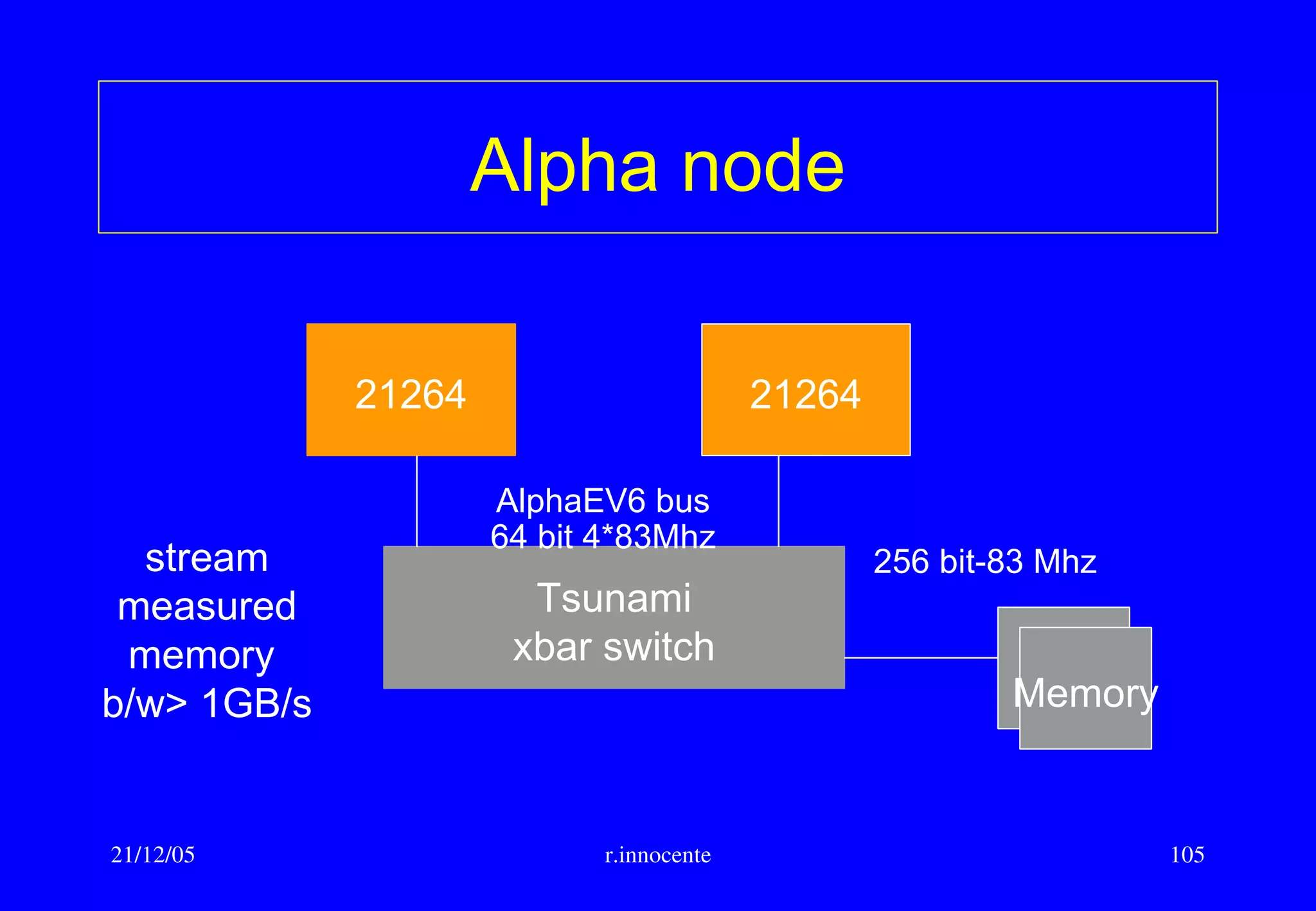
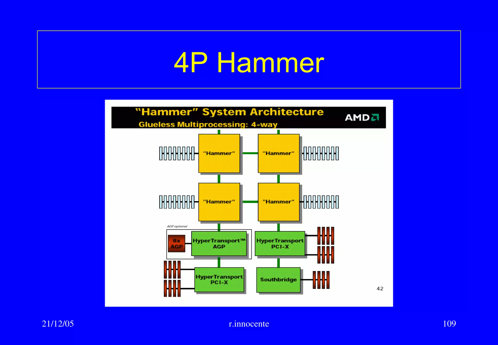
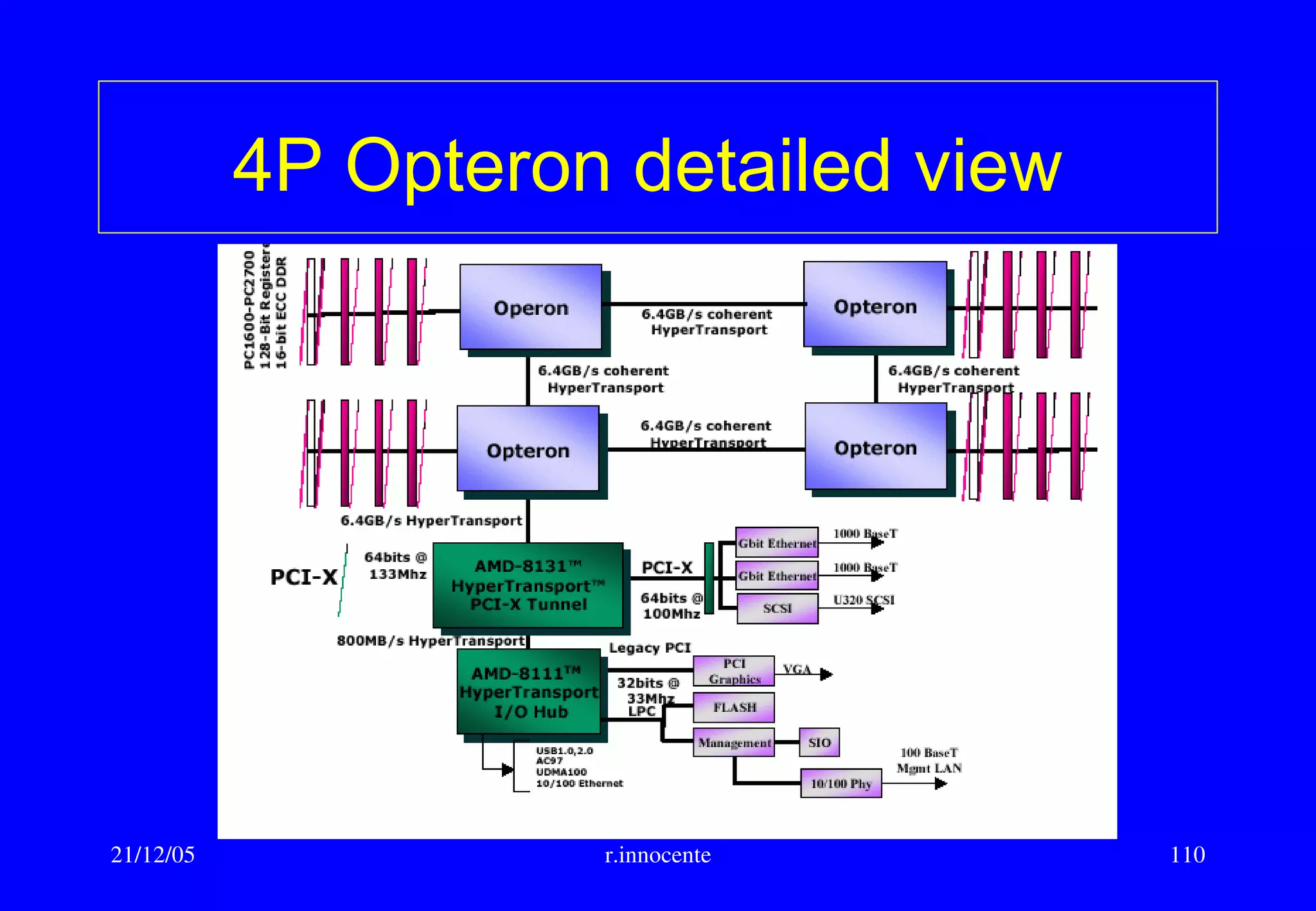
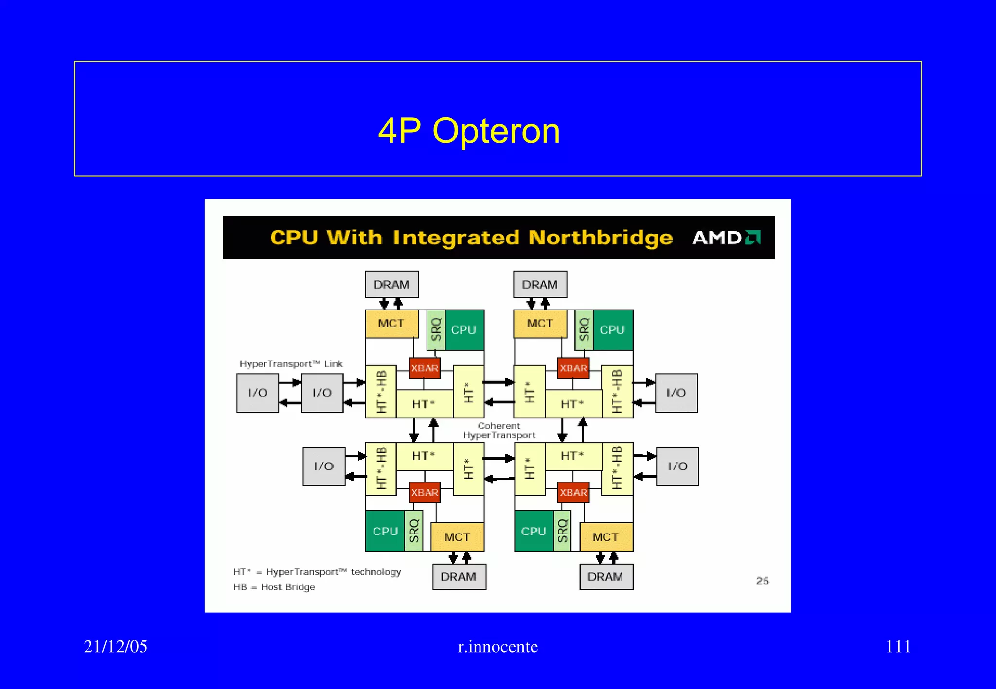
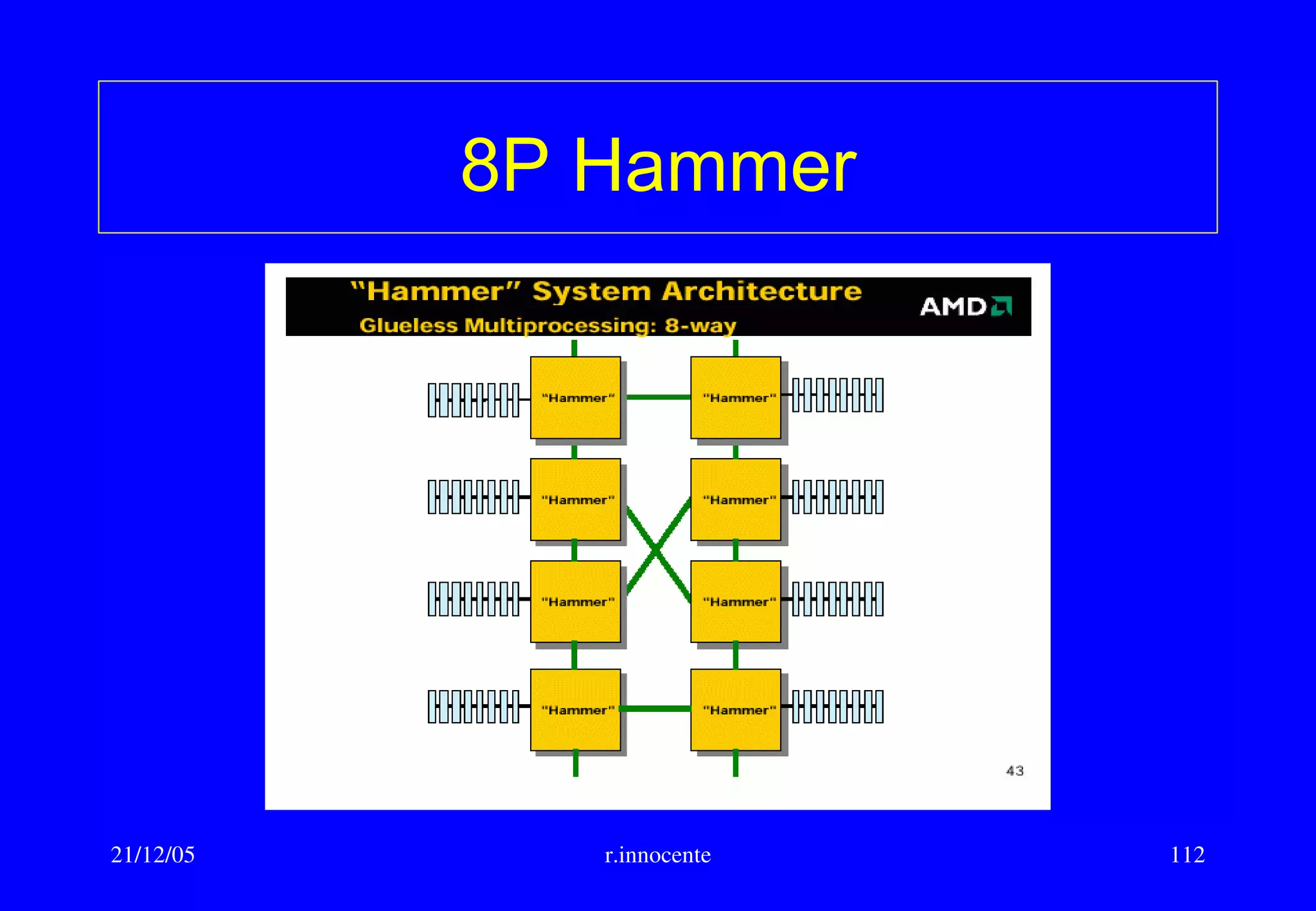
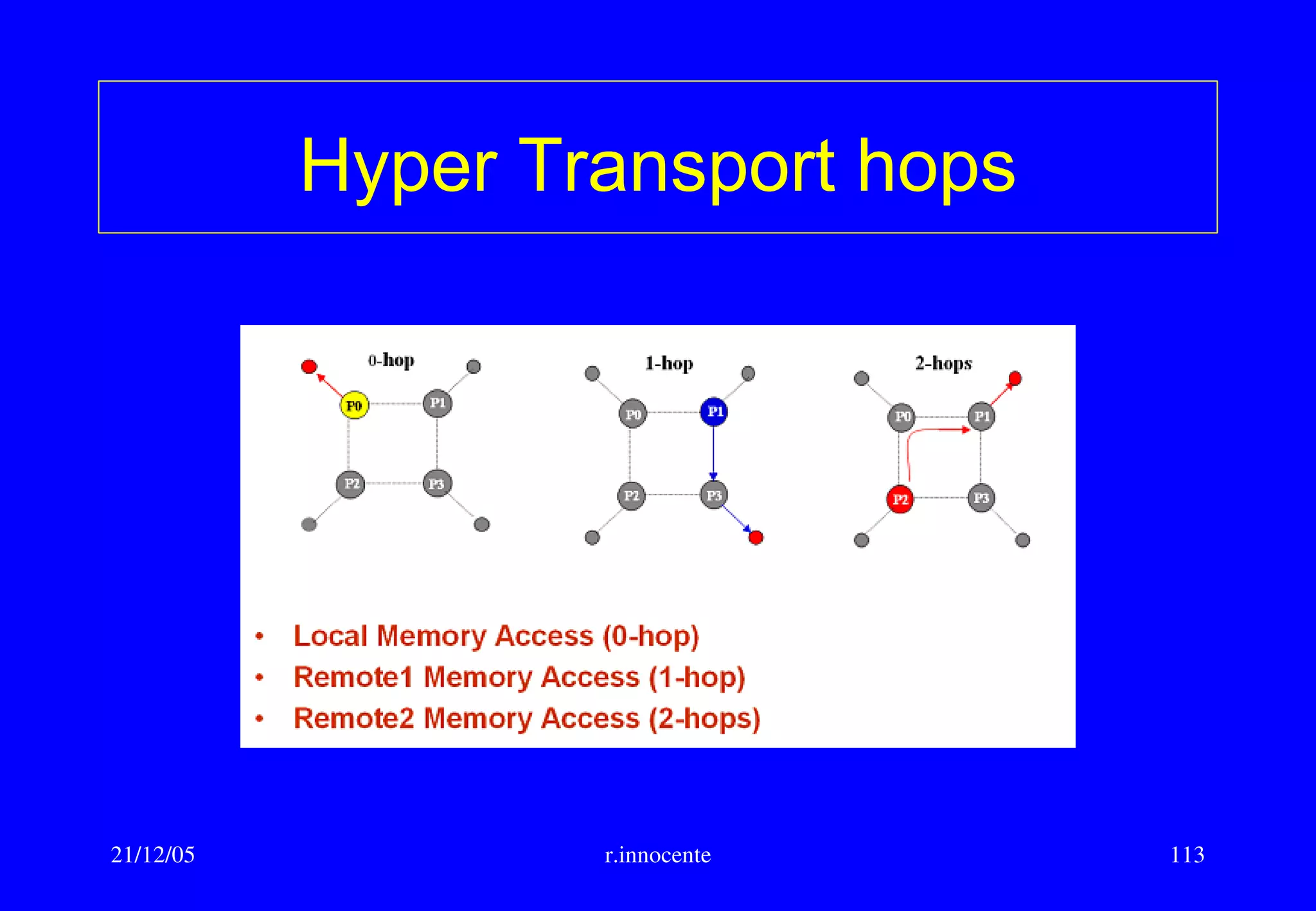
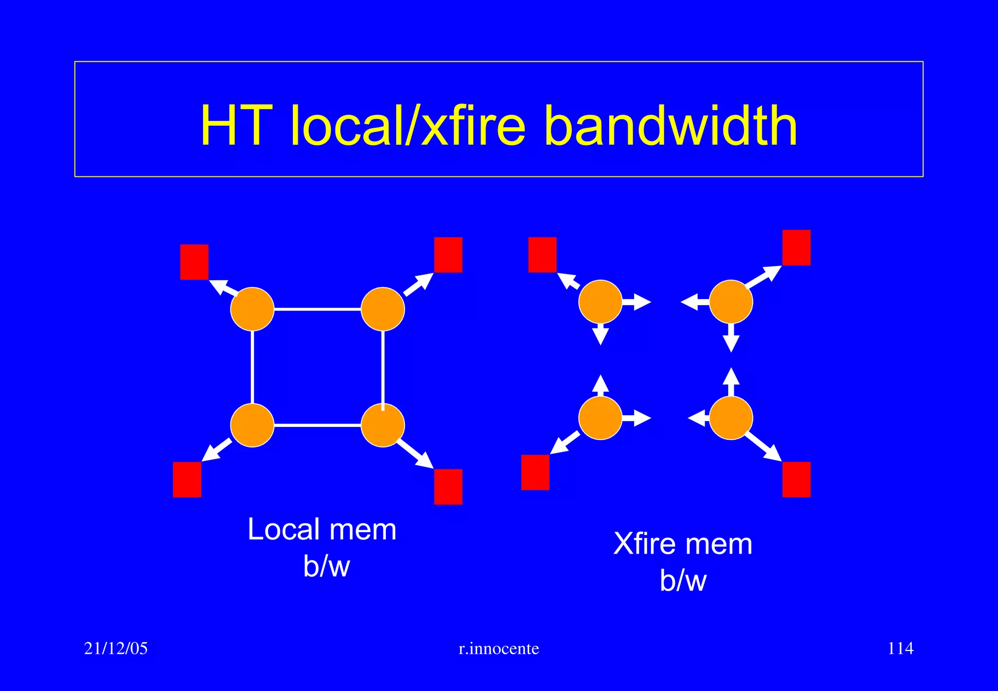
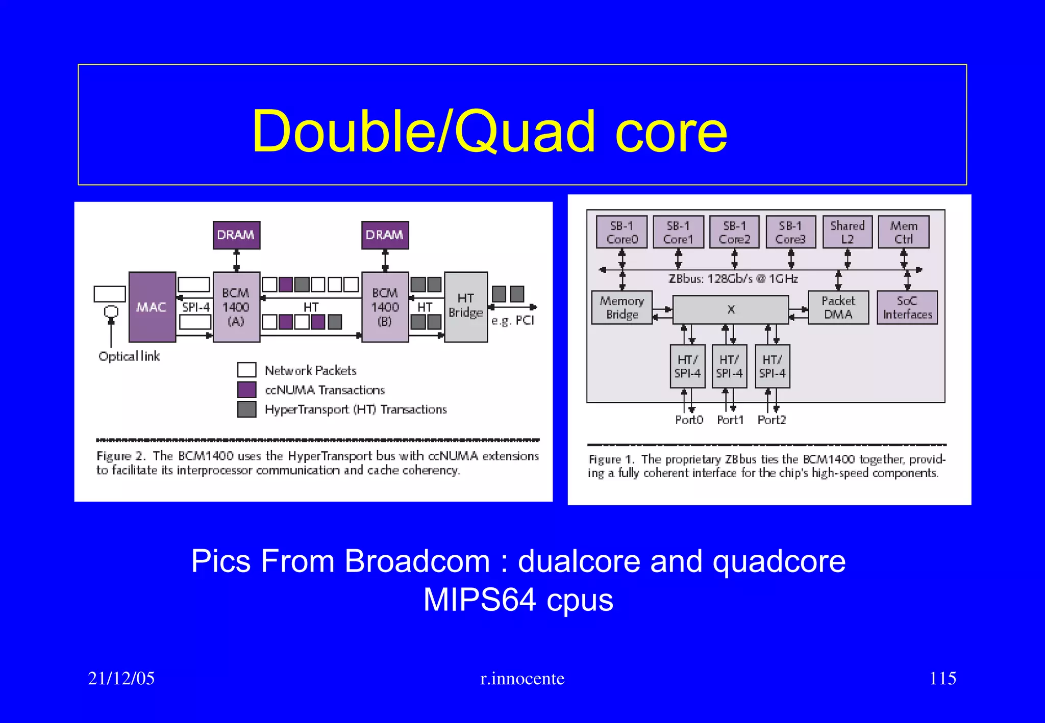
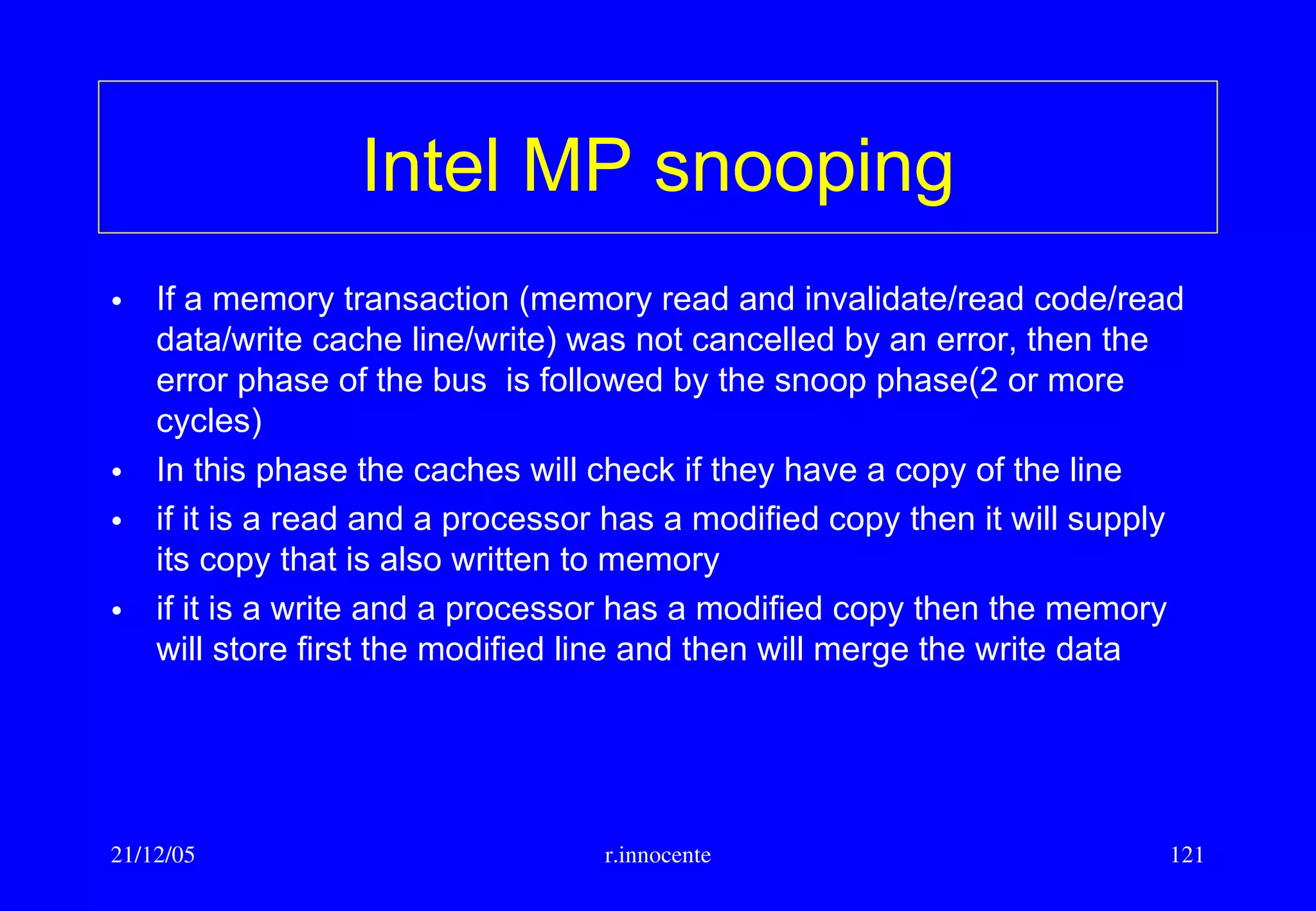
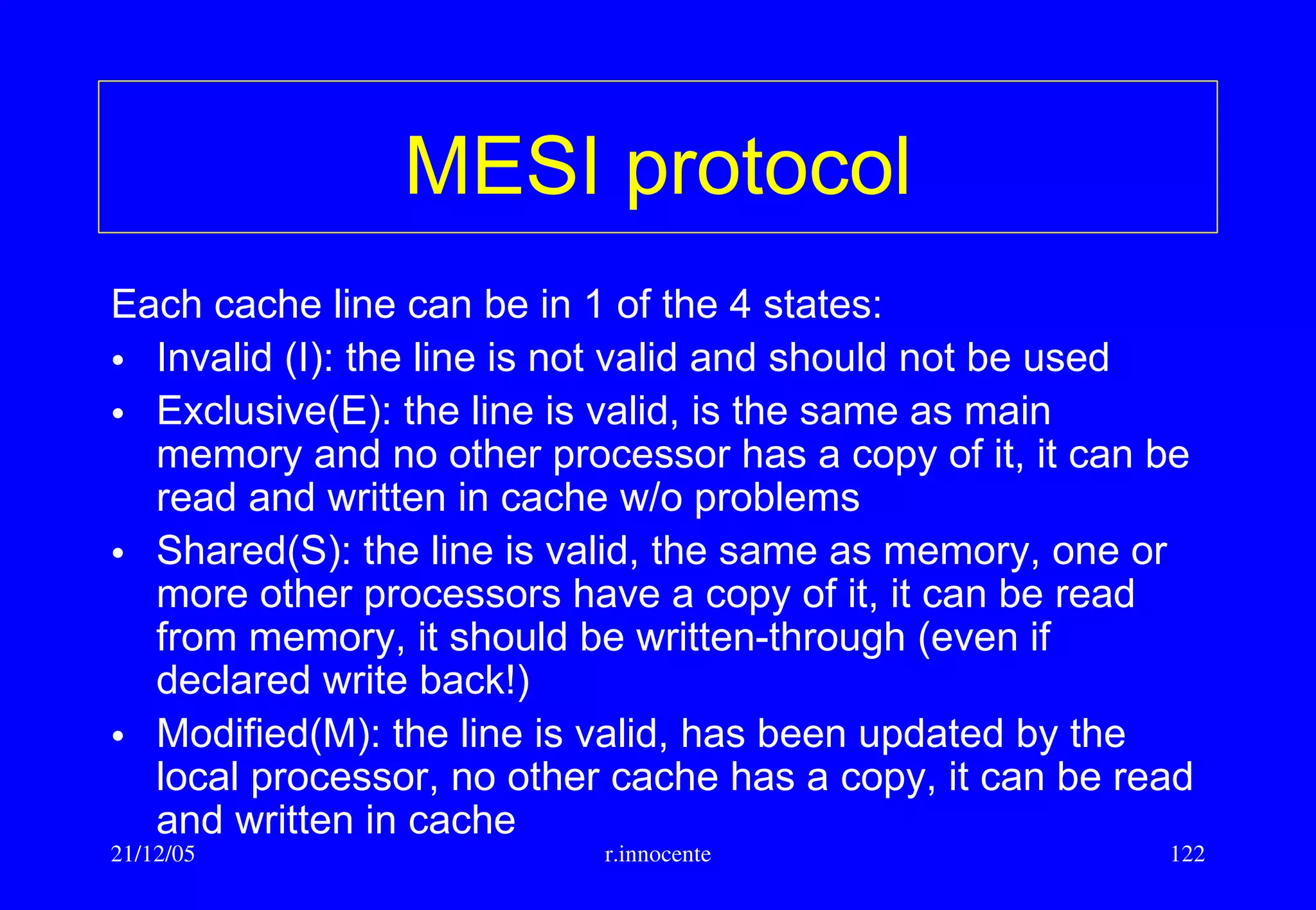
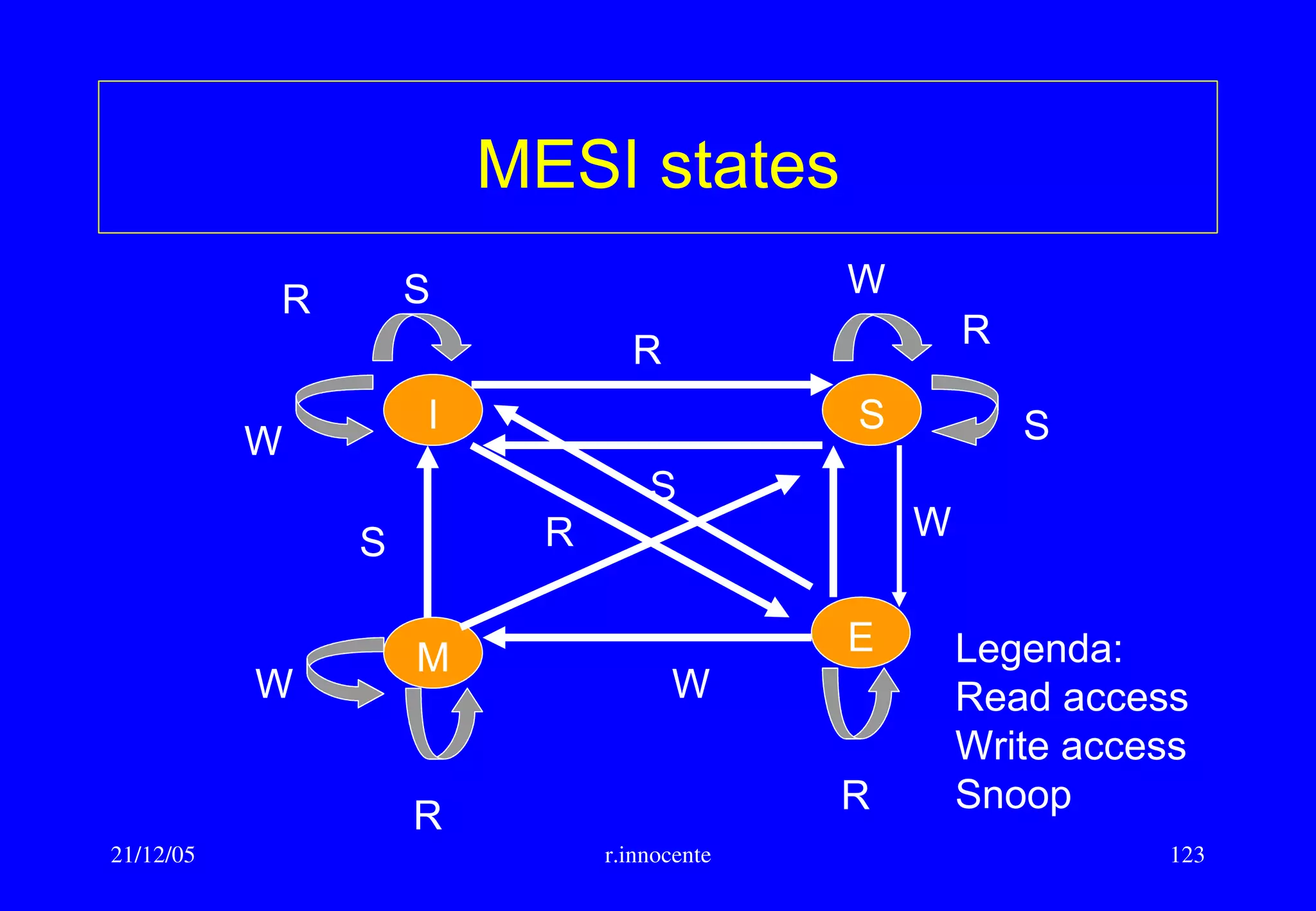
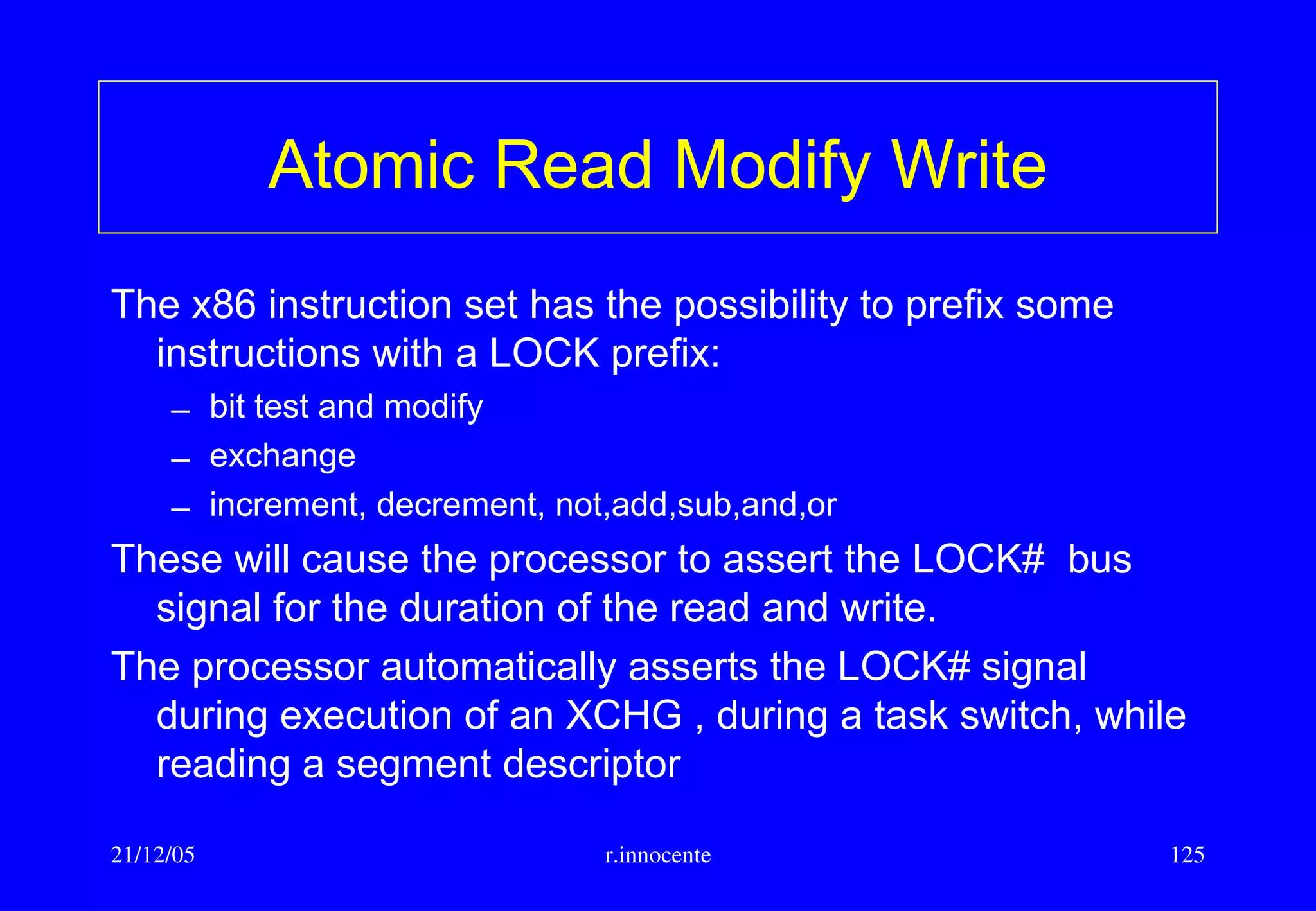
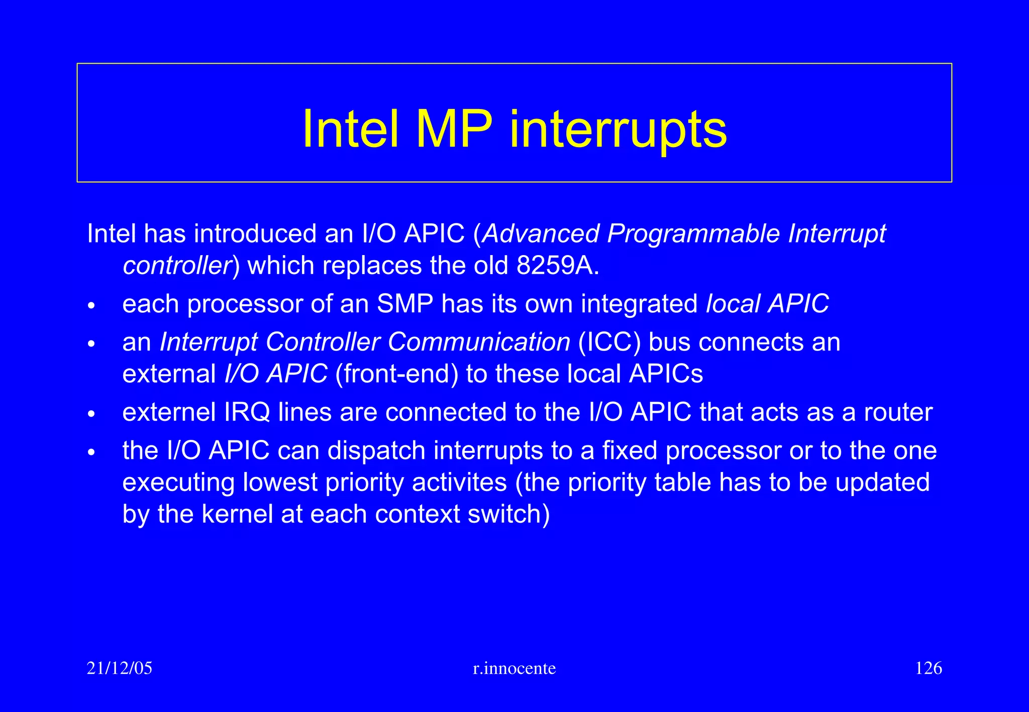
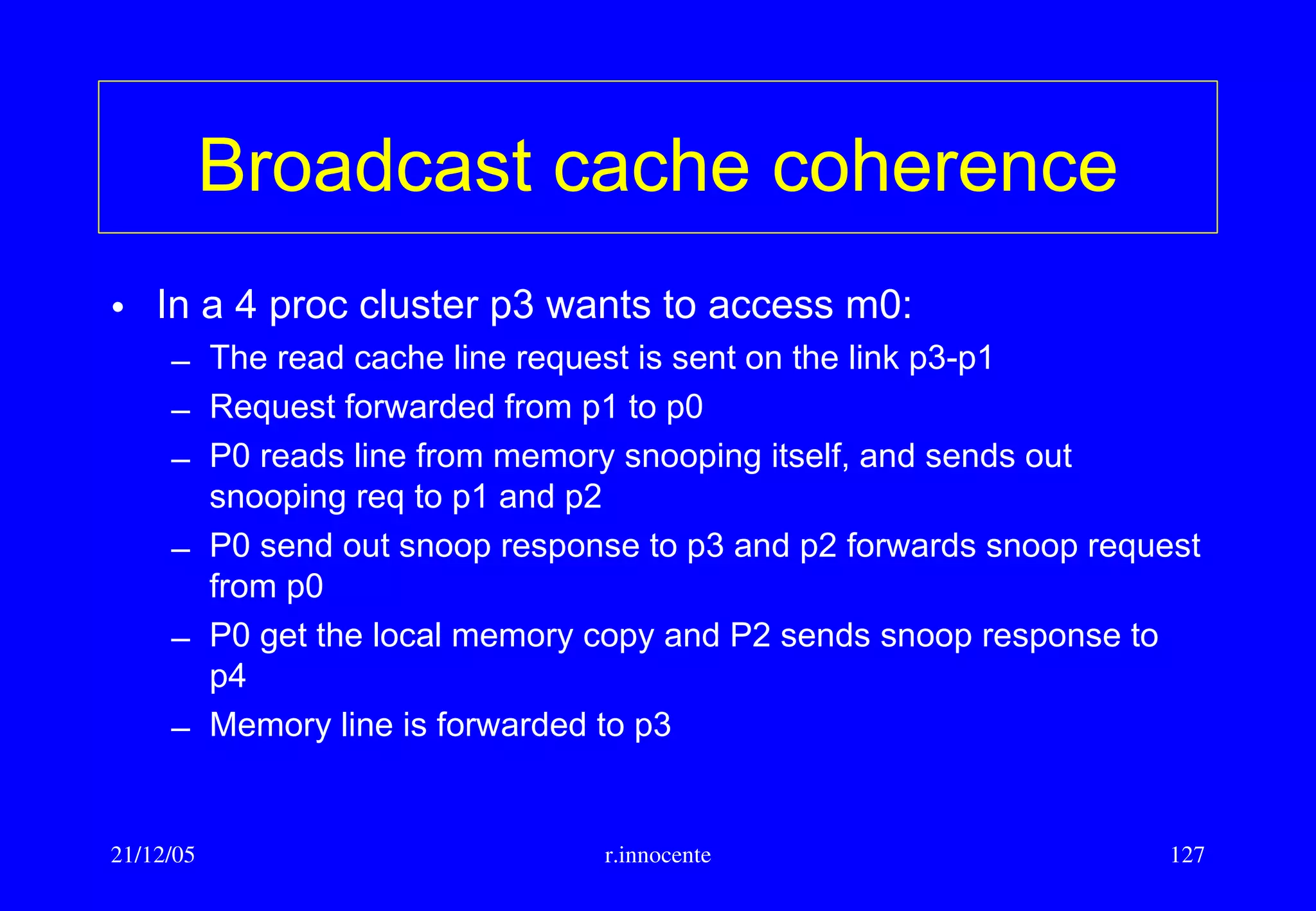
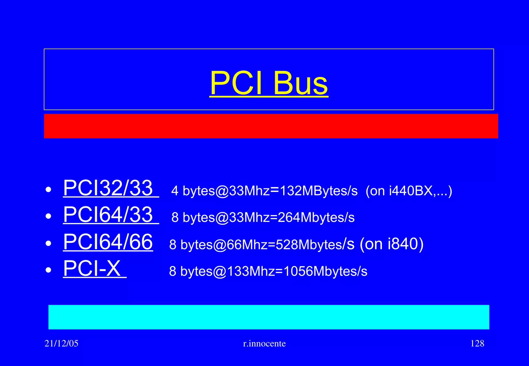
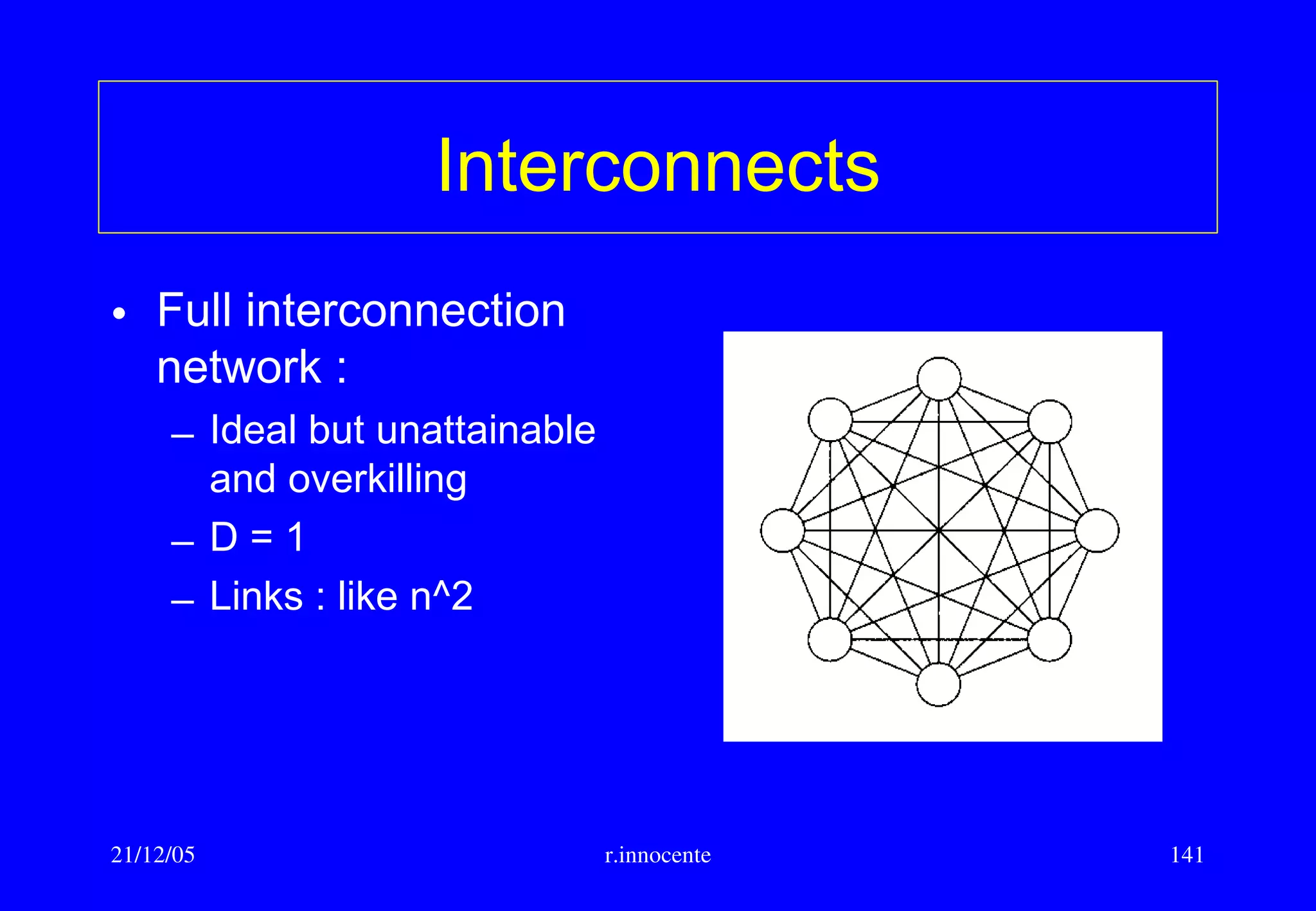
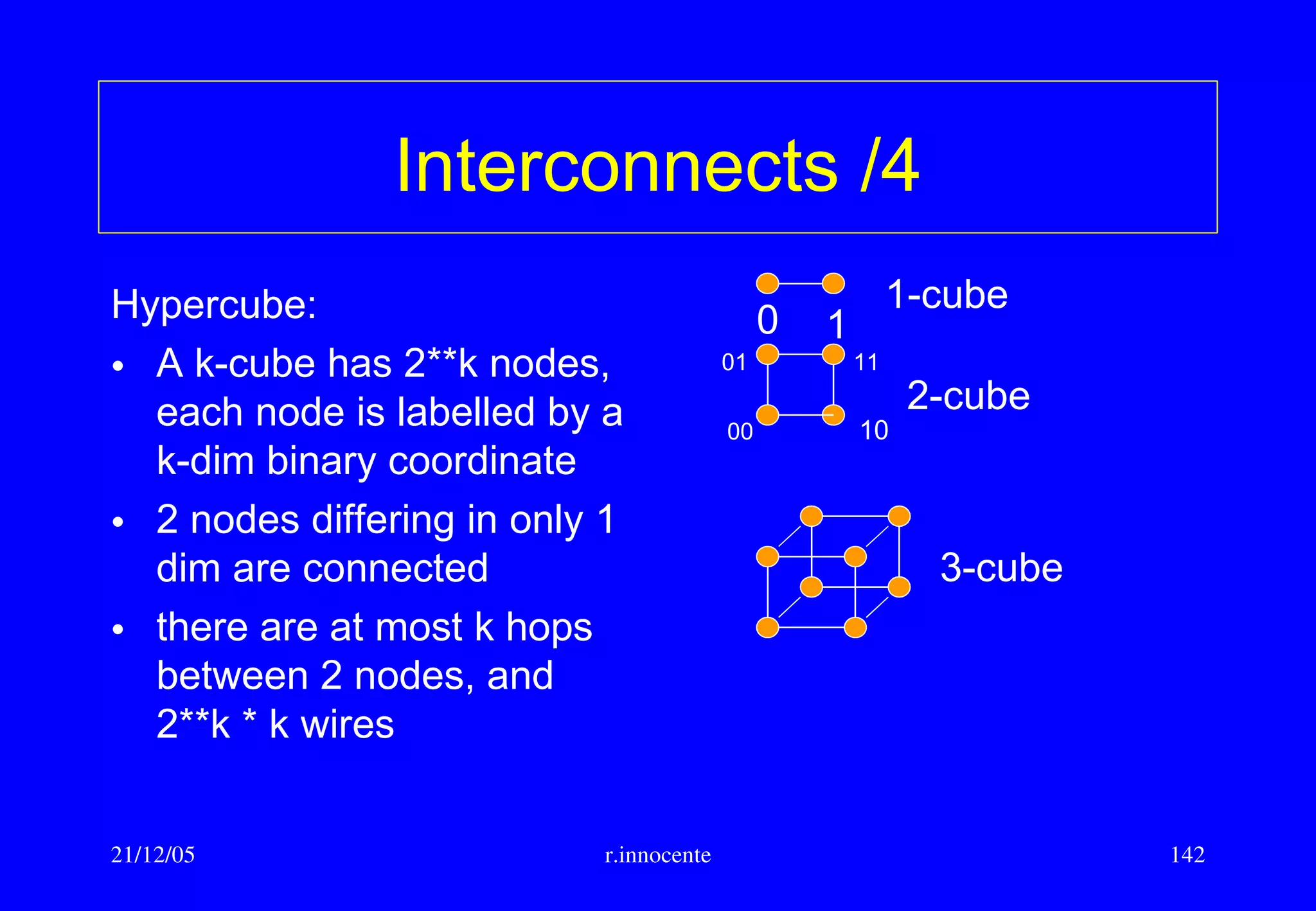
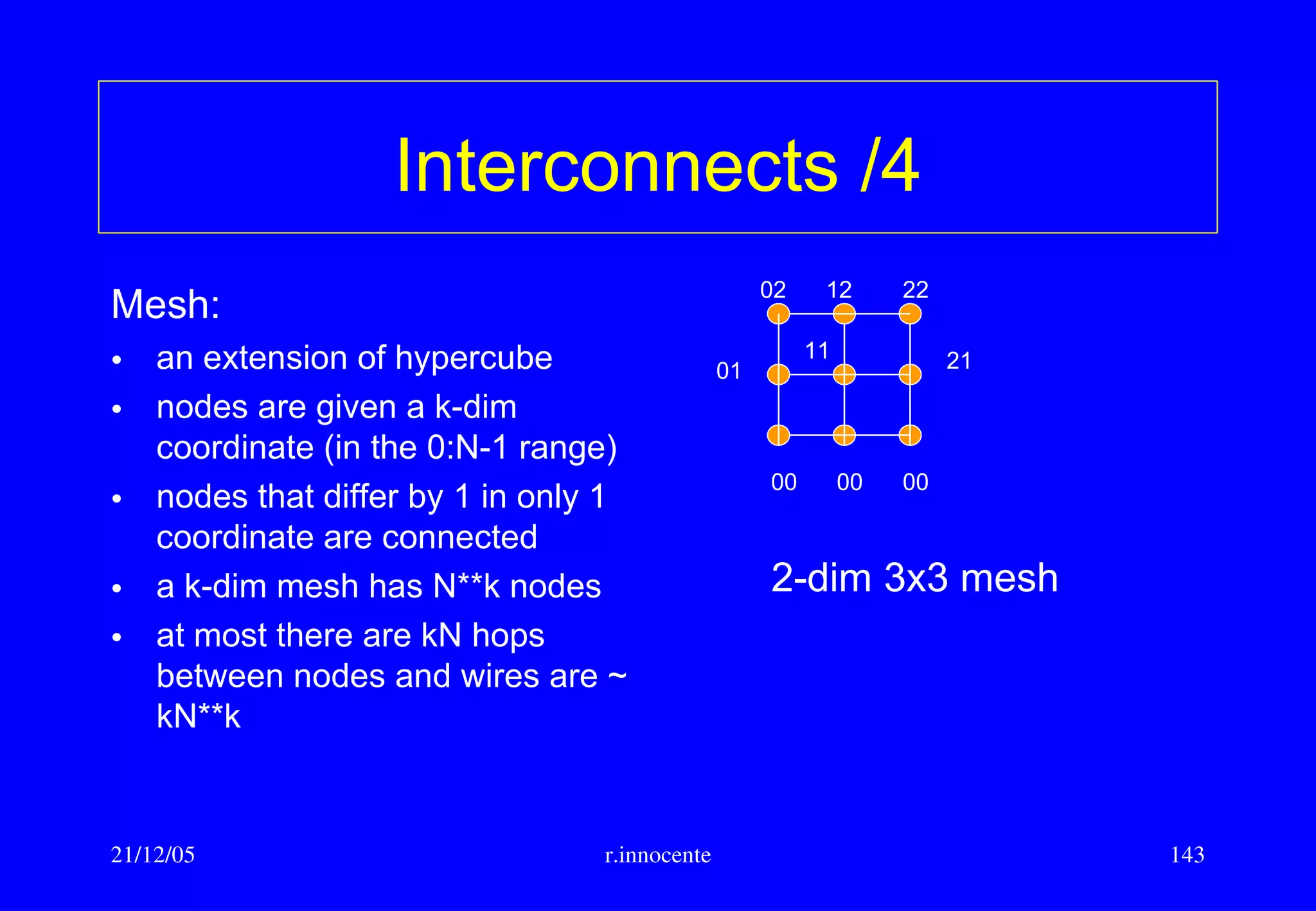
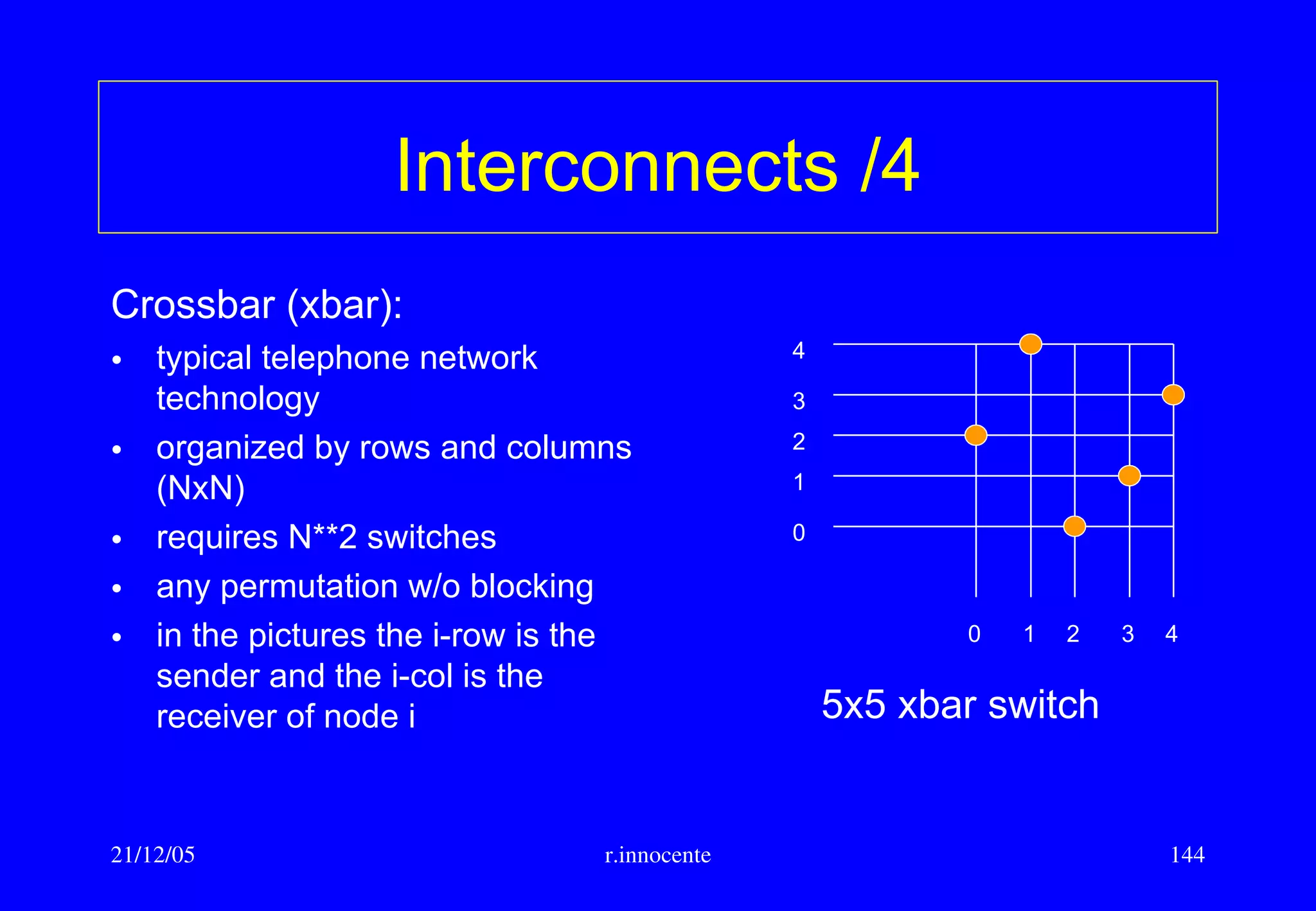
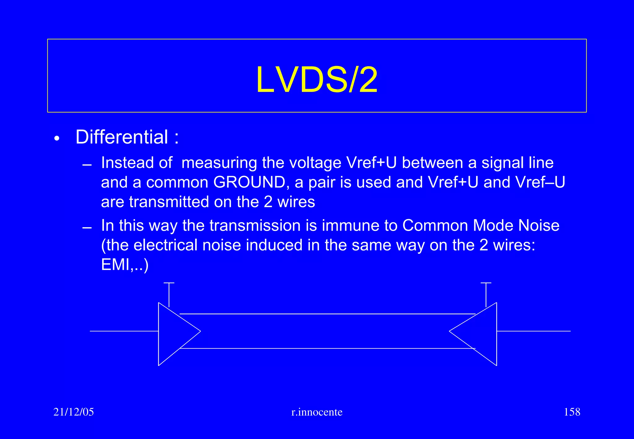
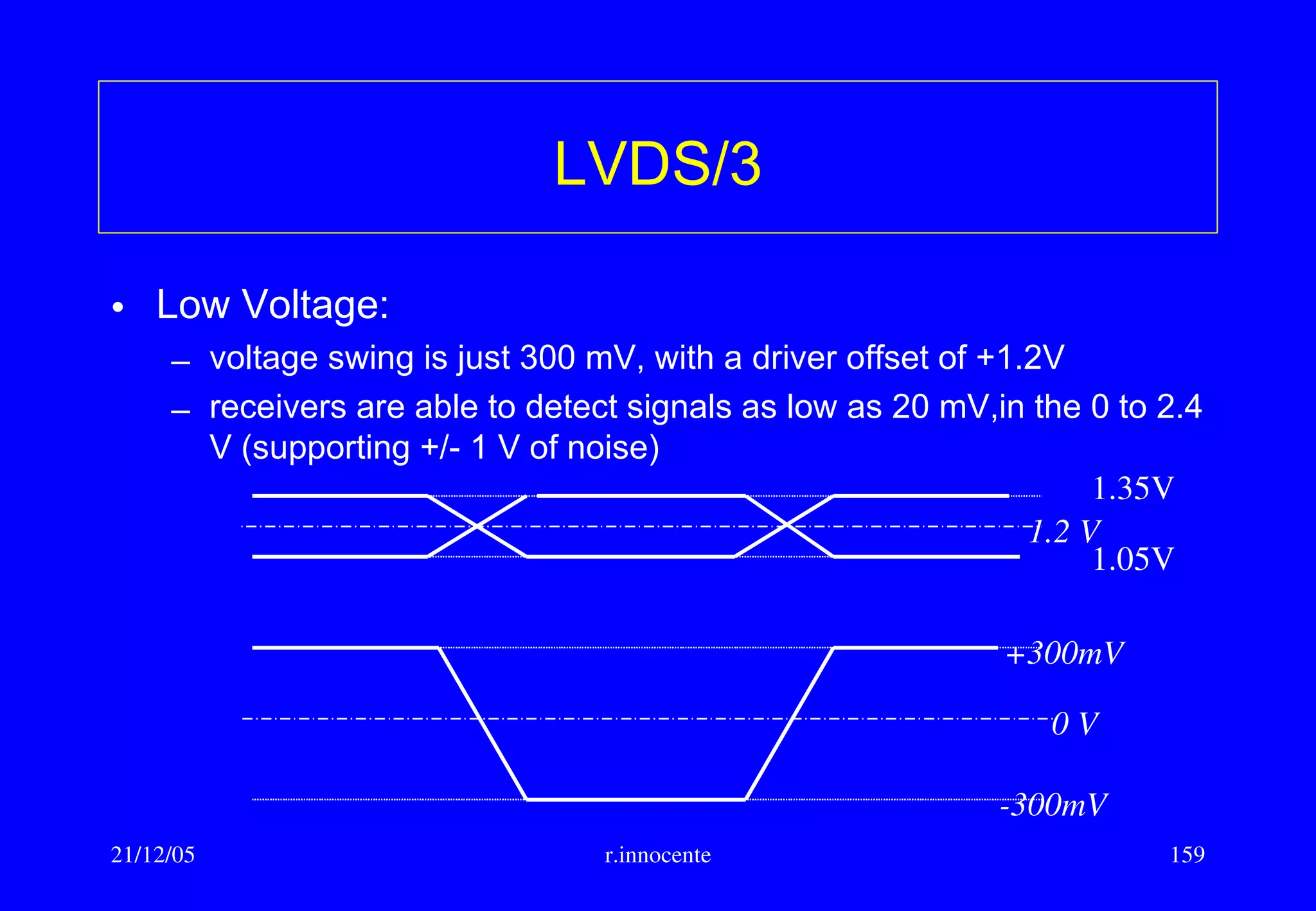
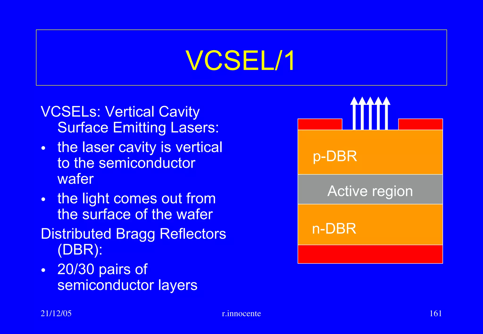
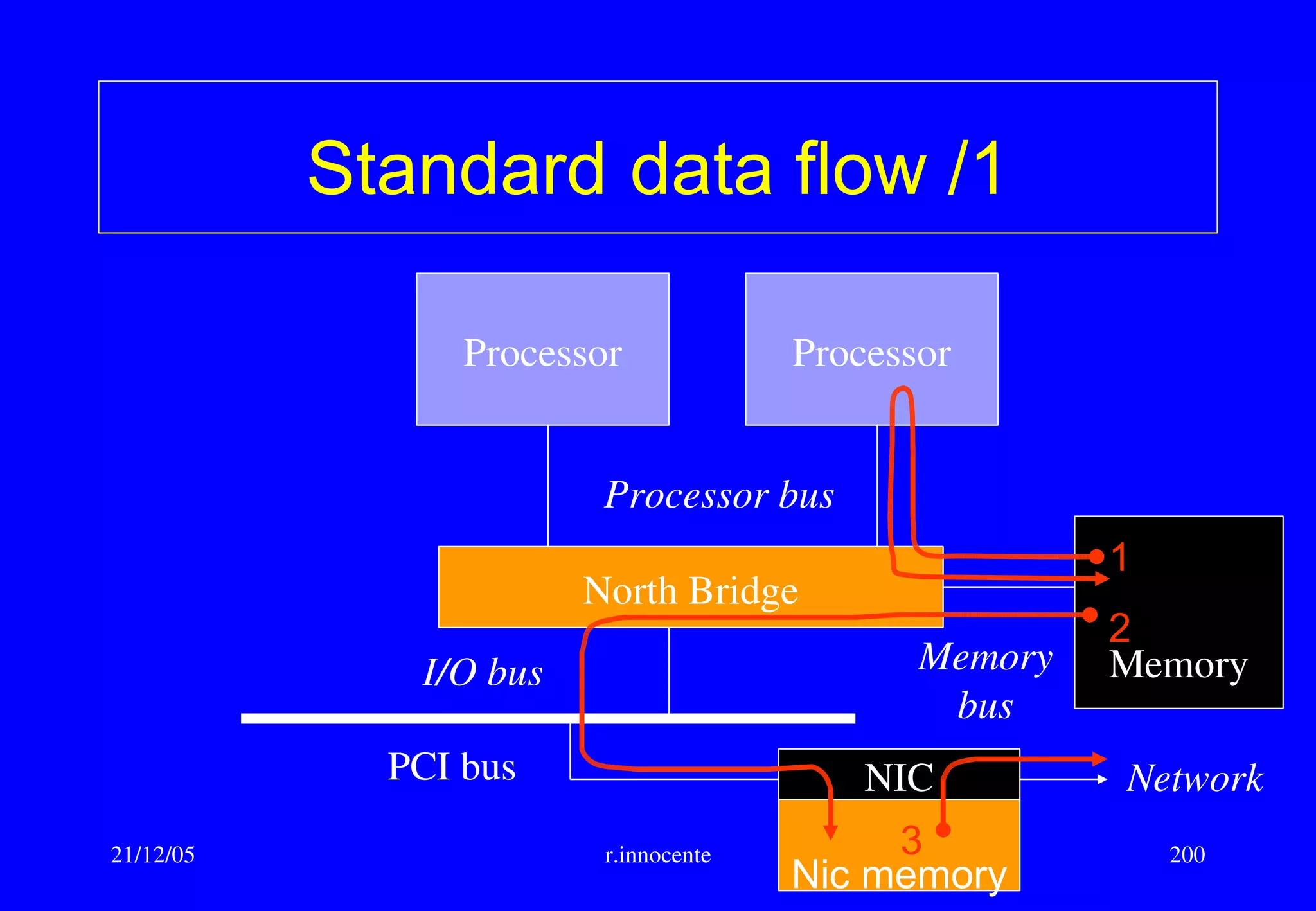
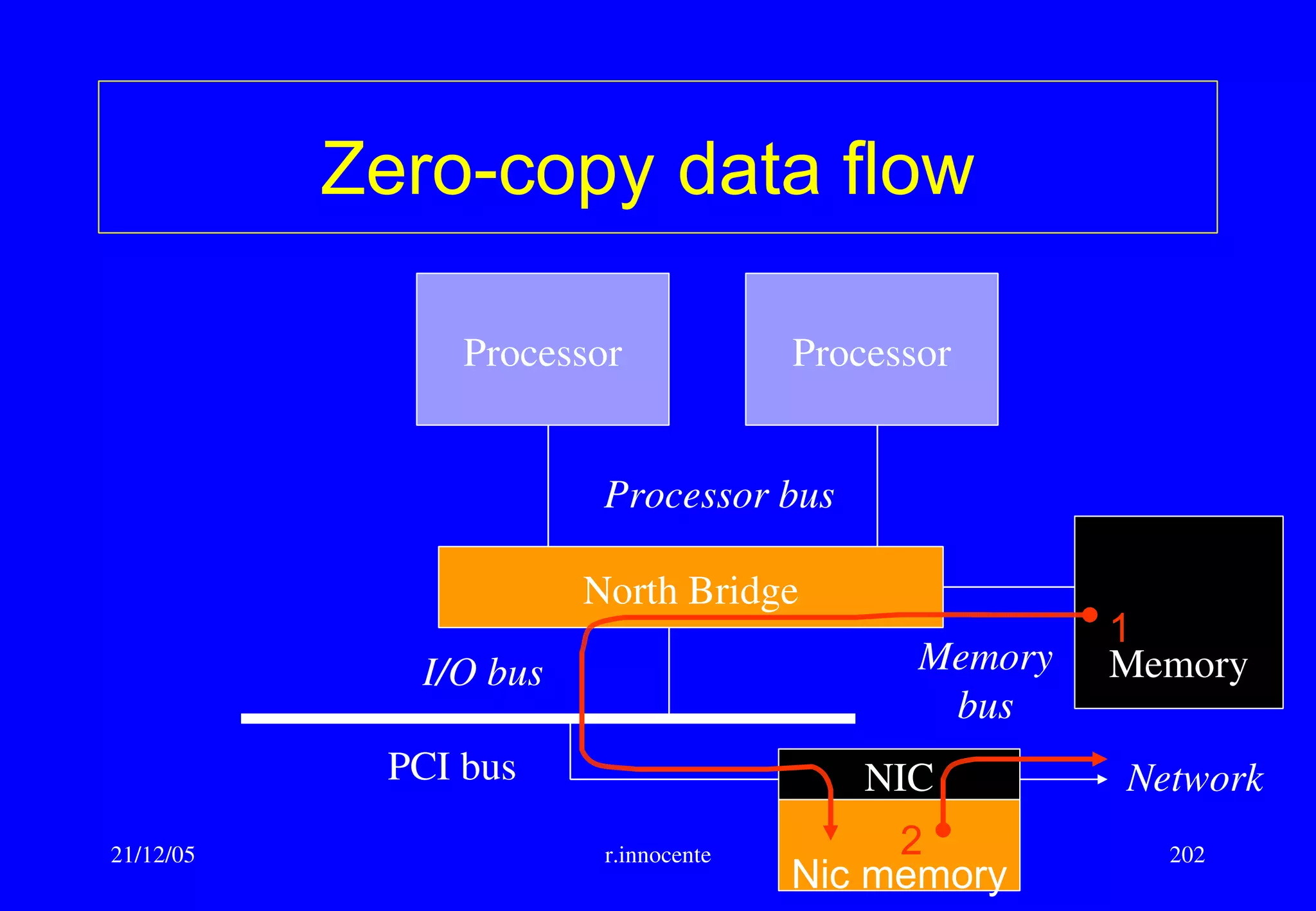
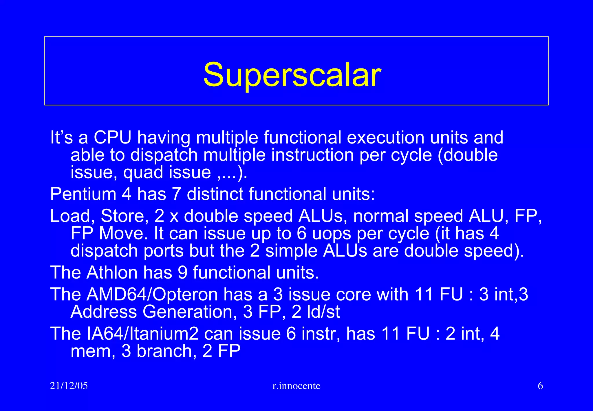
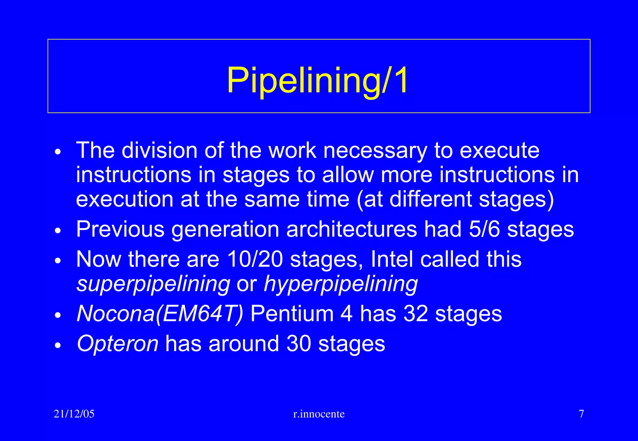
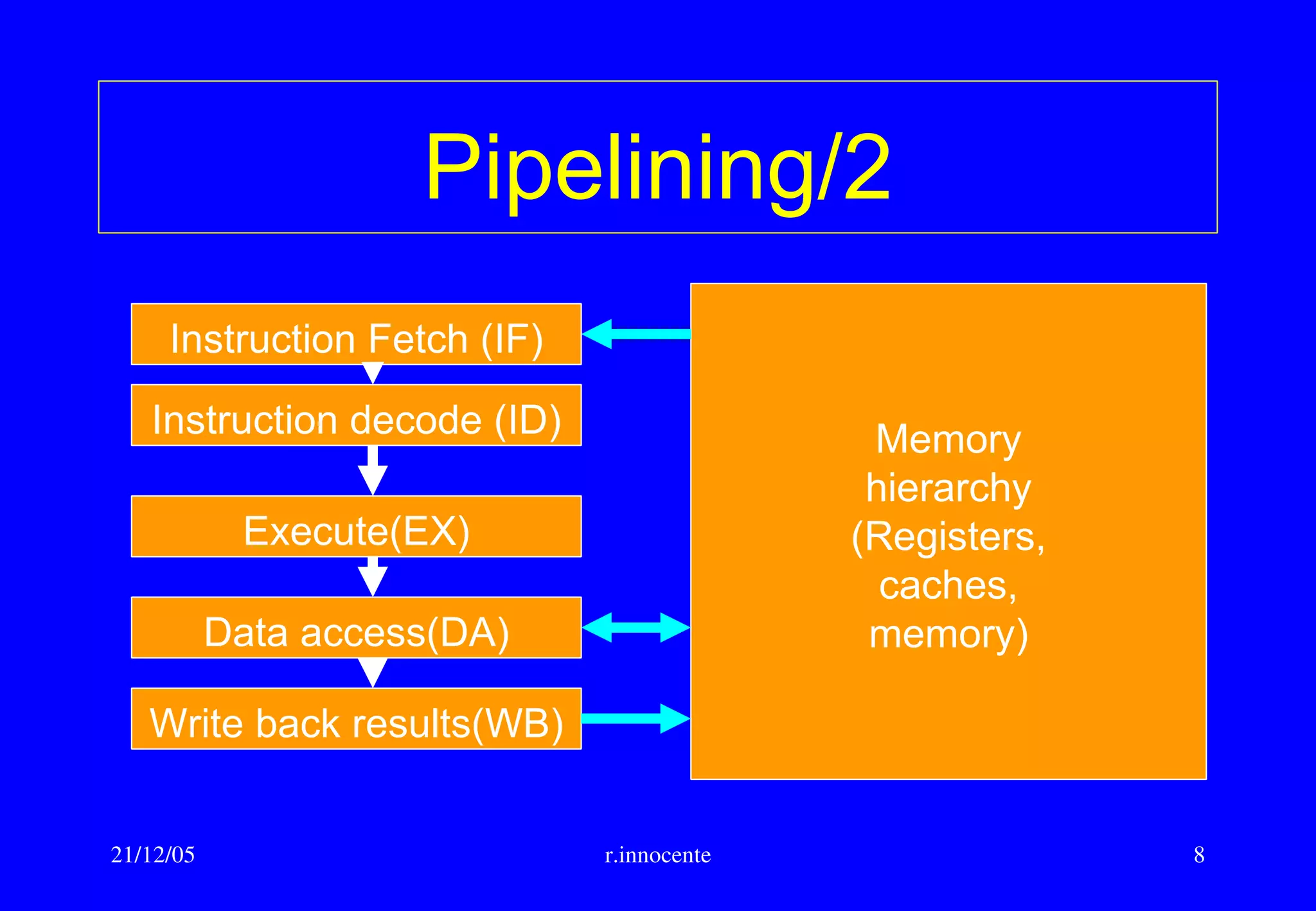
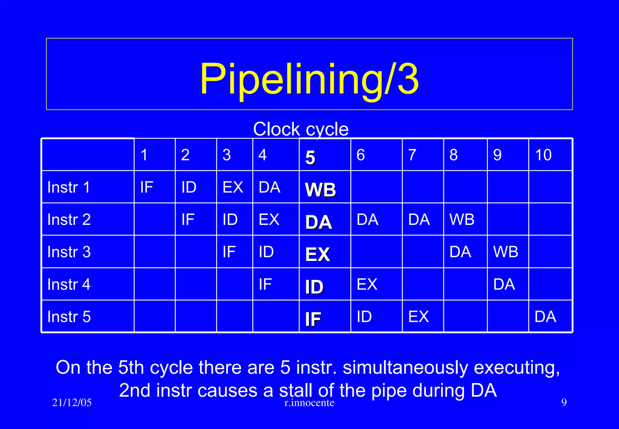
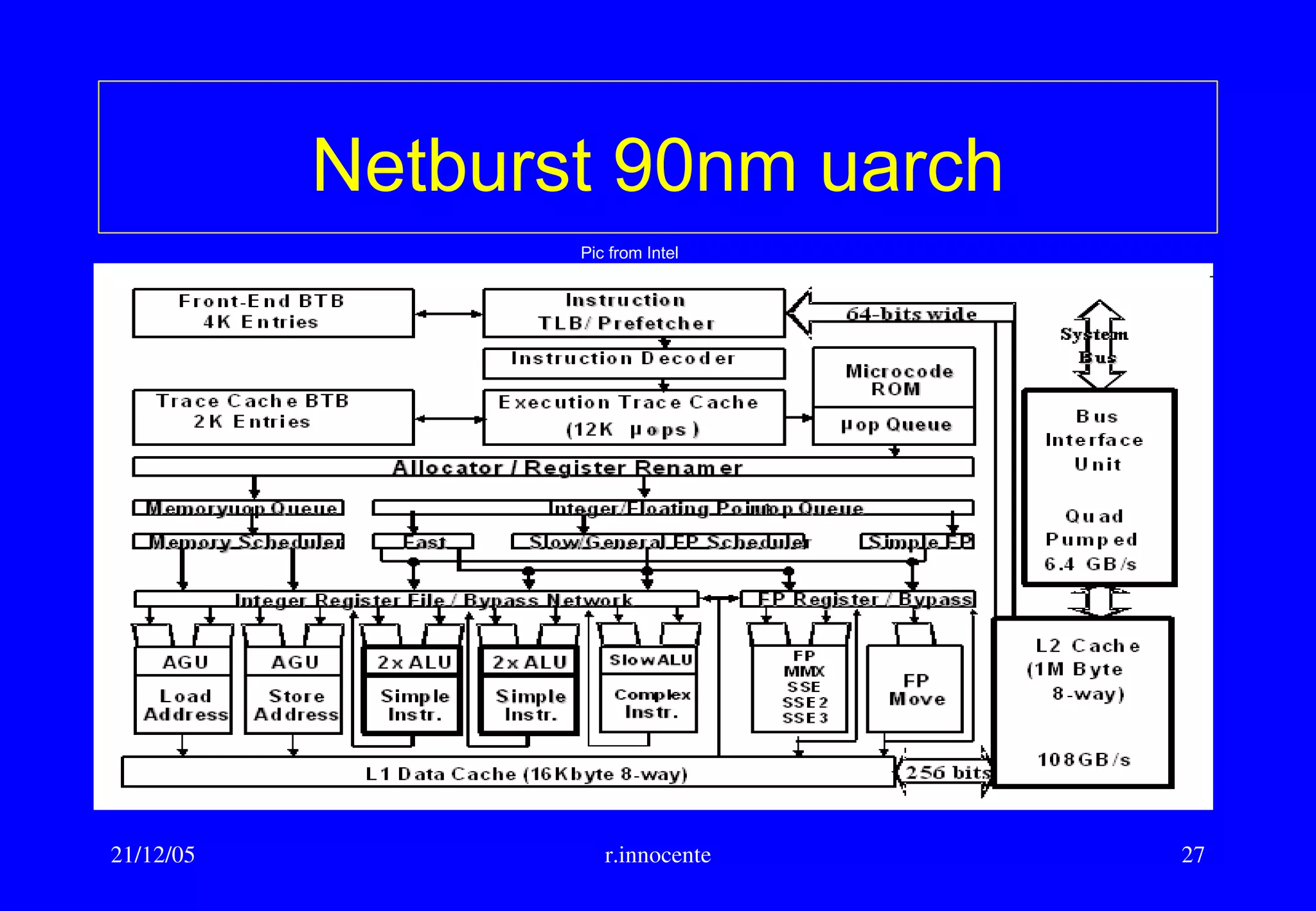
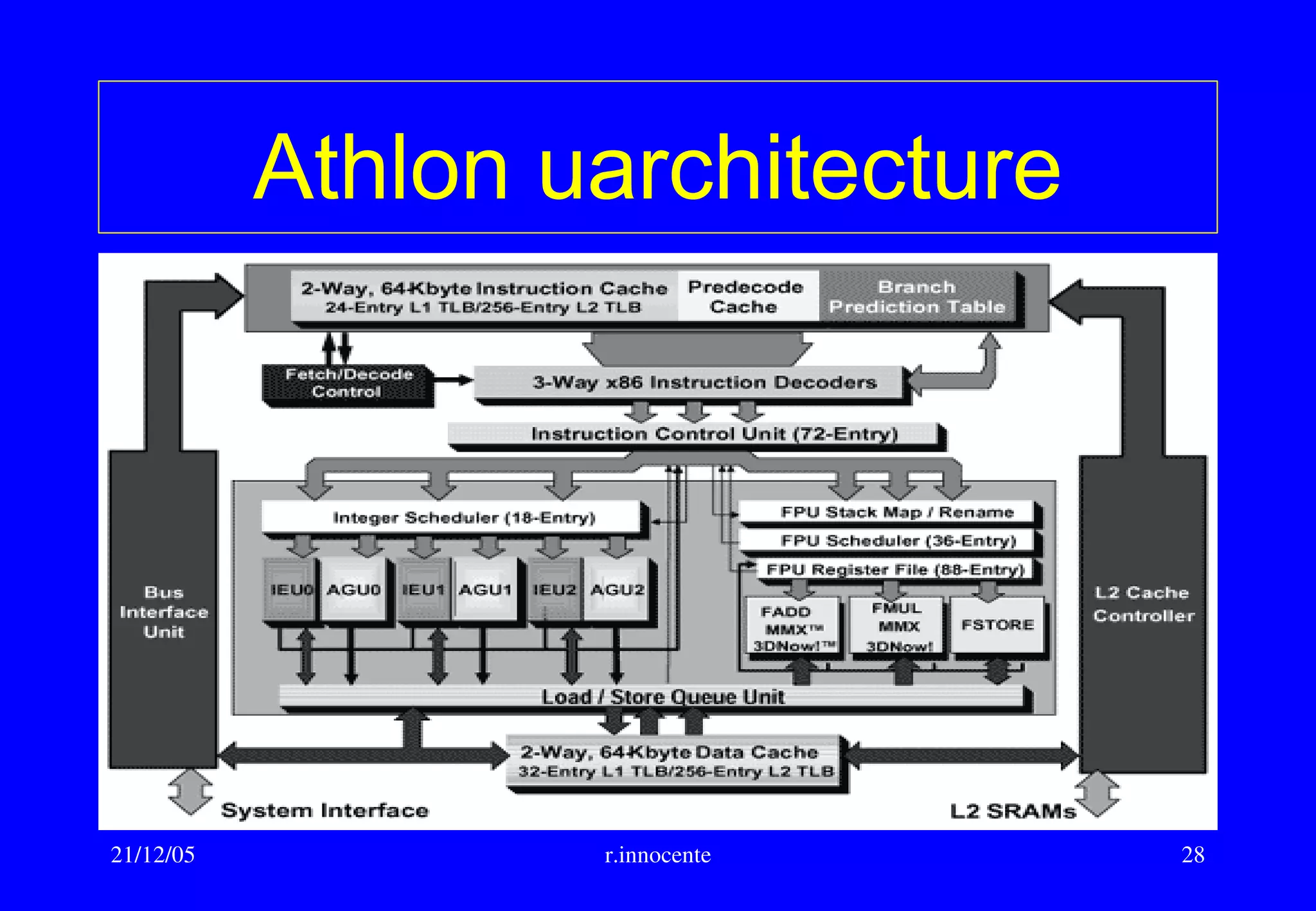
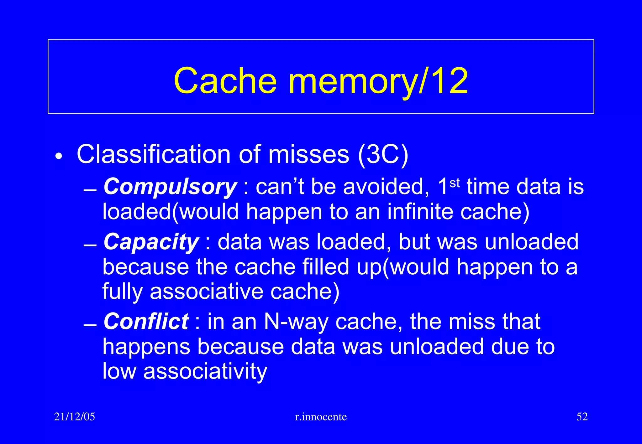
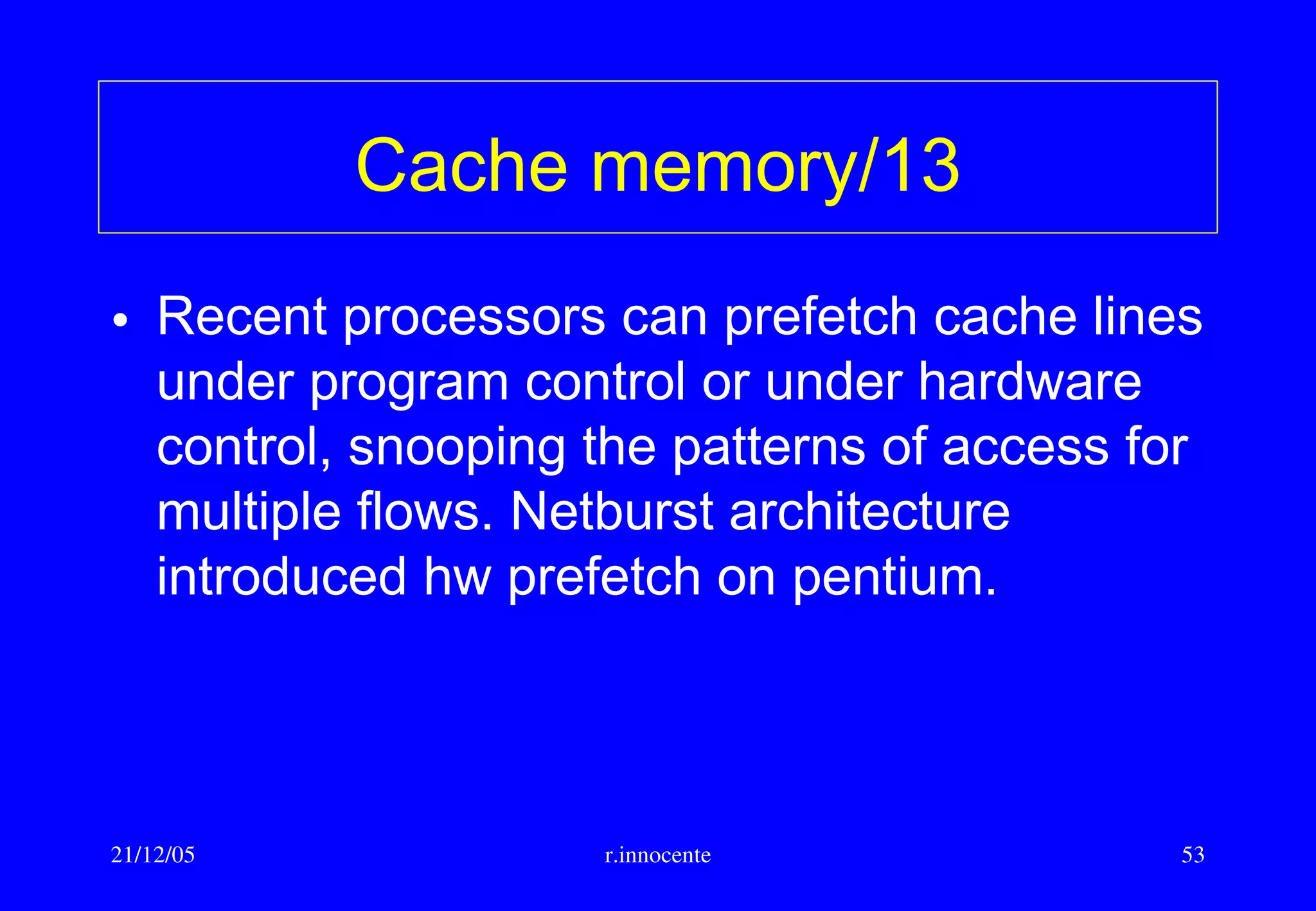
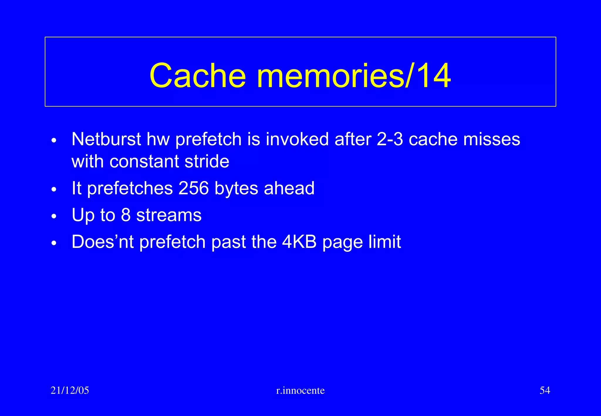
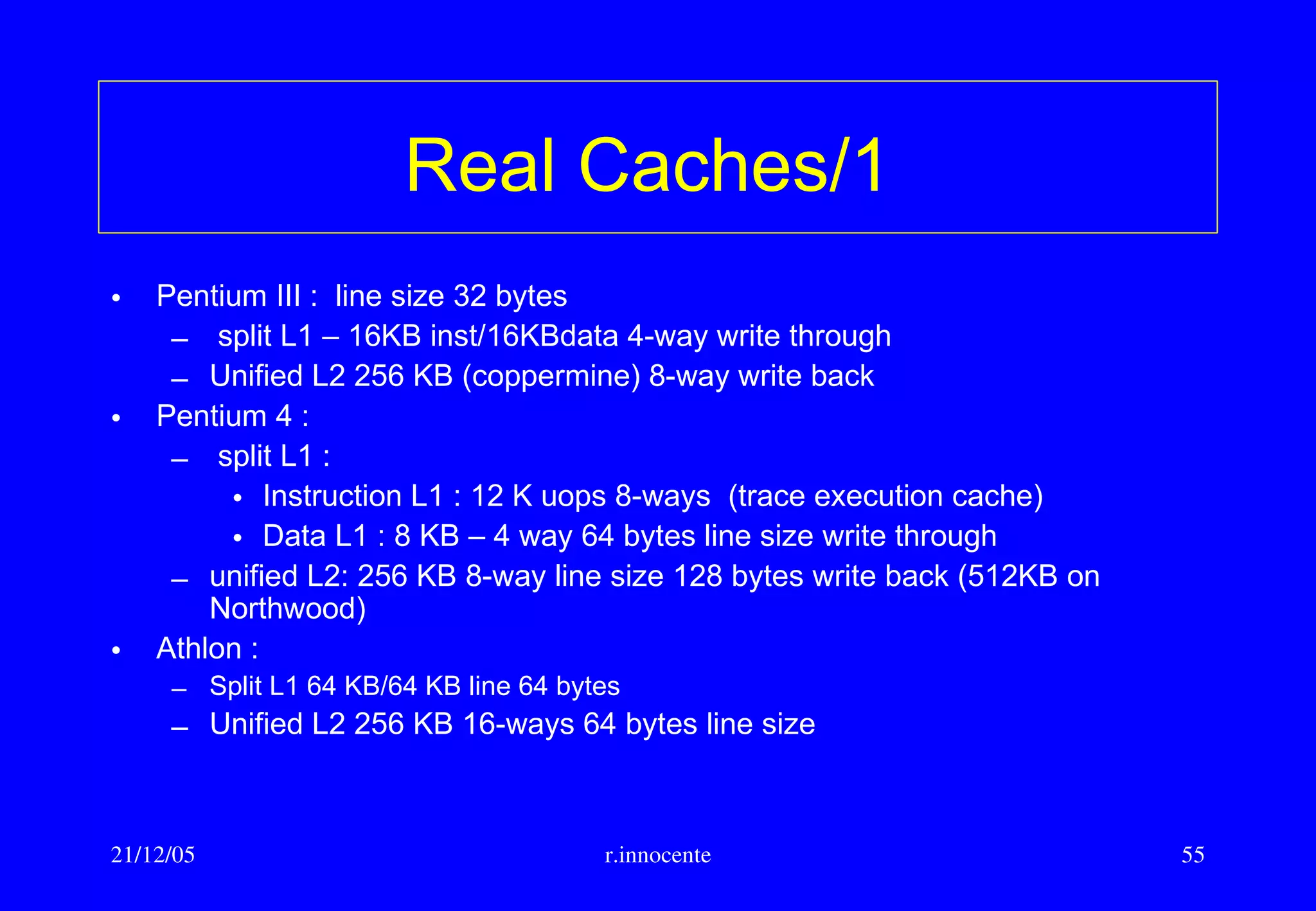
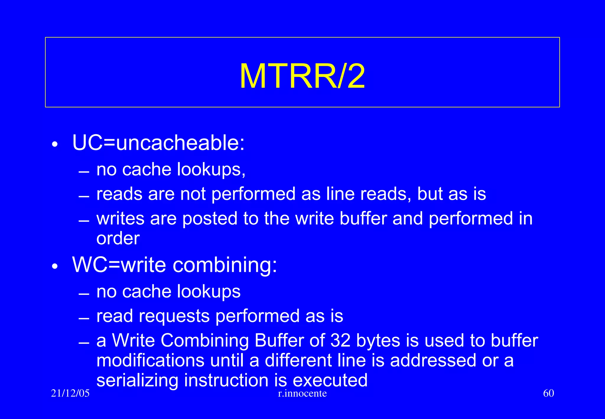
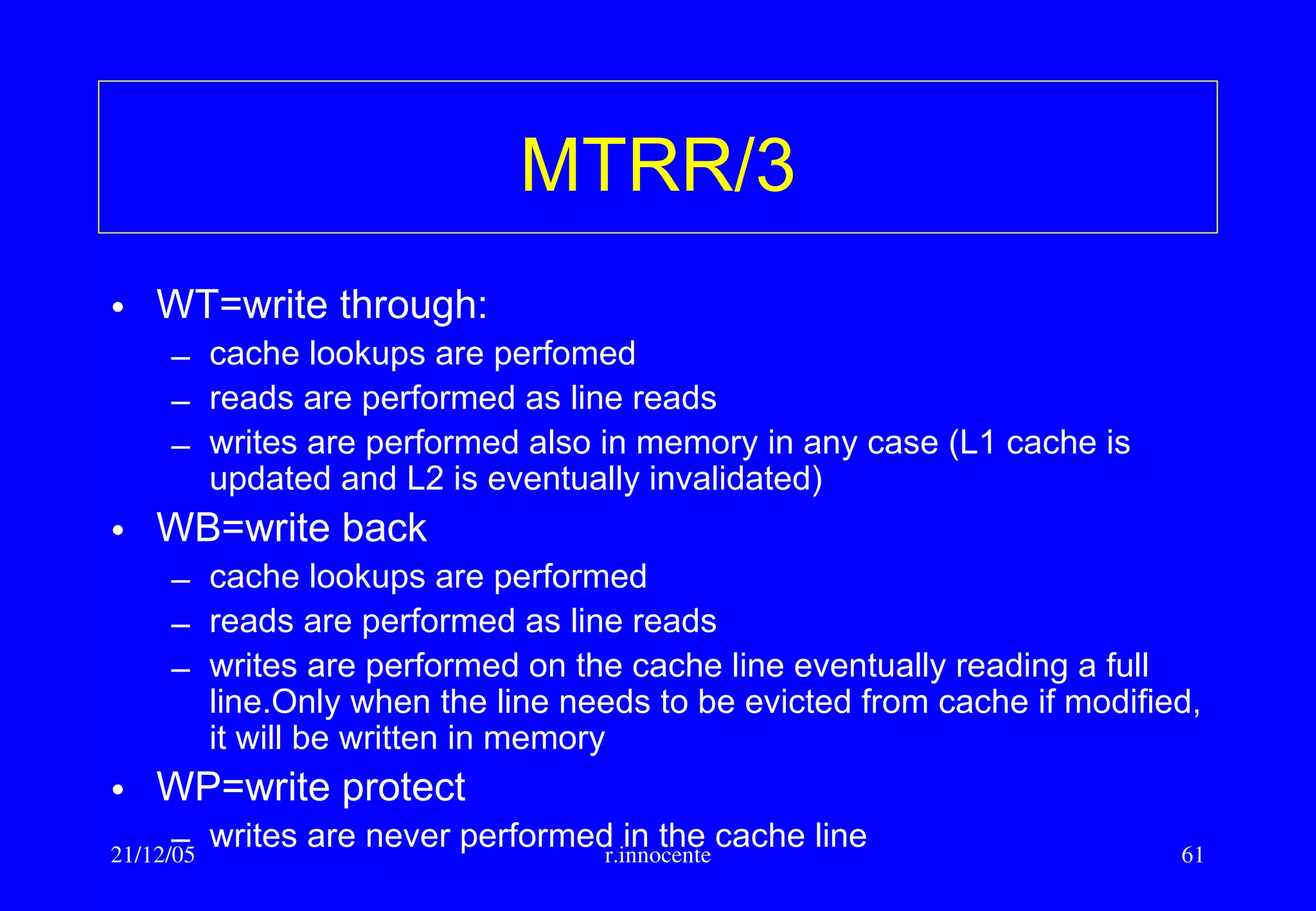
This document summarizes key aspects of computer hardware and architecture. It discusses nodes and networks that make up computer systems. It describes different types of computer instruction sets like CISC and RISC. It outlines various microarchitecture features for high performance computing like superscalar, pipelining, out-of-order execution, and branch prediction. It also covers cache memory organization and algorithms.

![21/12/05 r.innocente 45
Cache memory/5
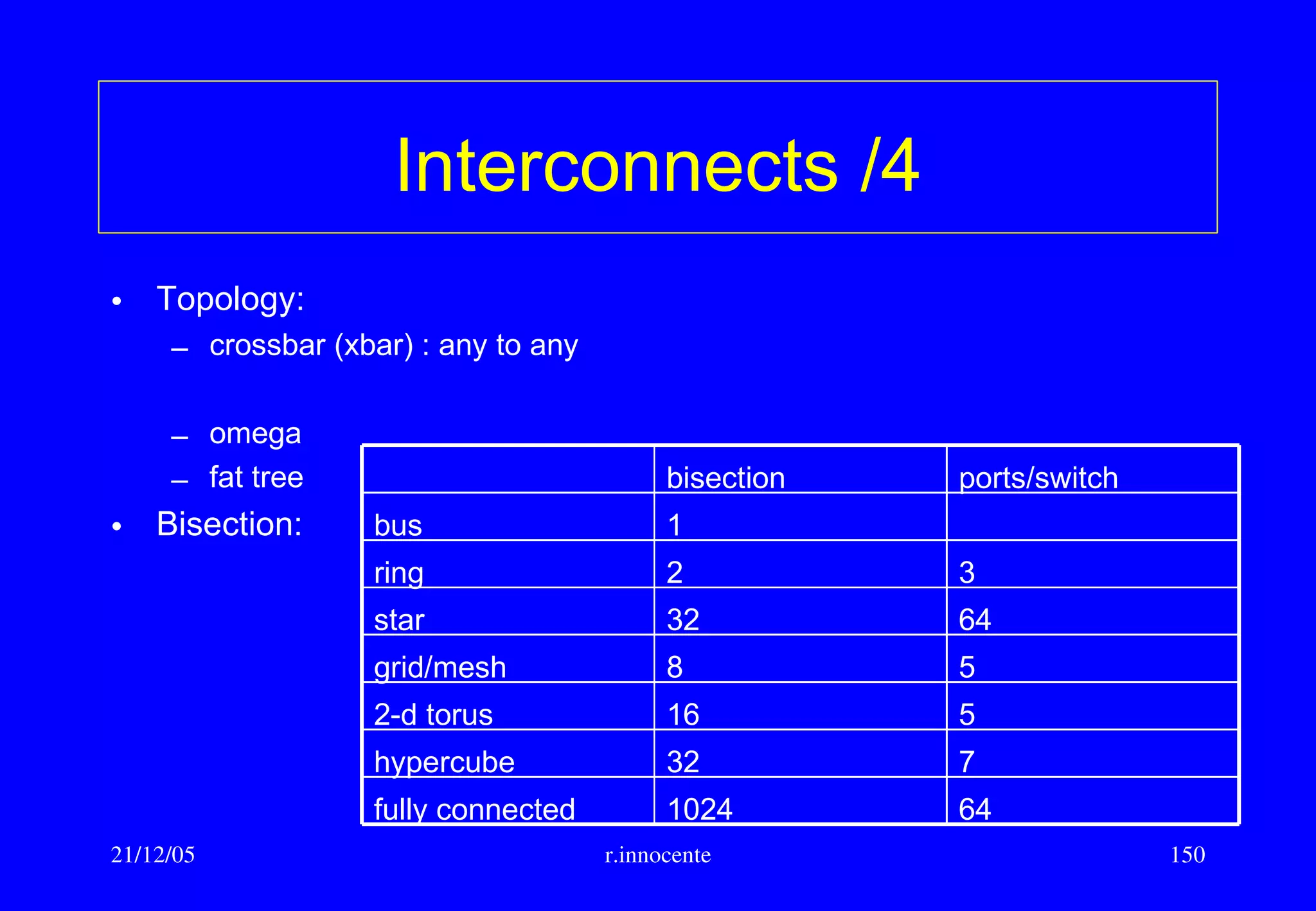
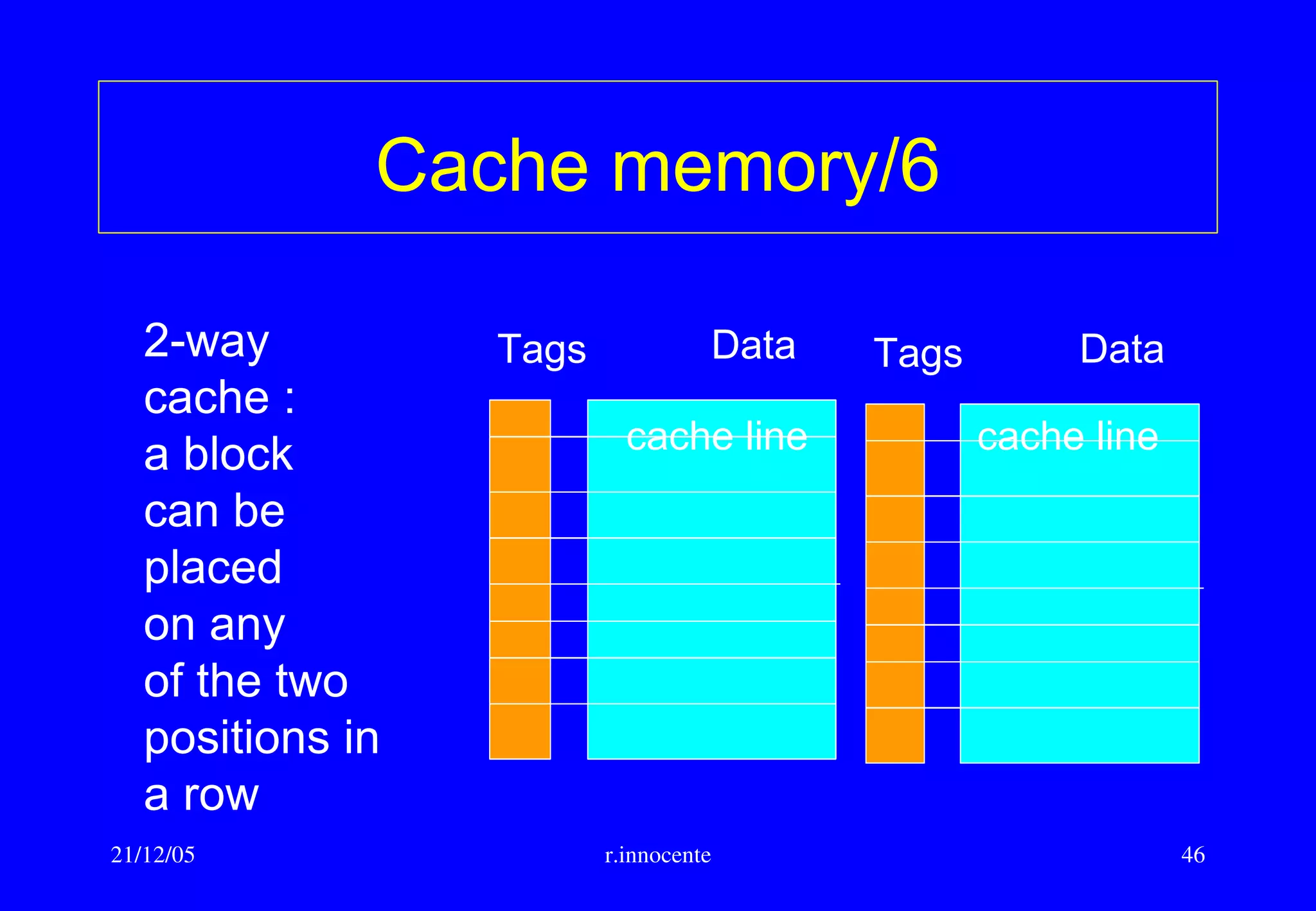
Block placement algorithm :
• Direct Mapped : a block can be placed in just one row of the cache
• Fully Associative : a block can be placed on any row
• n-Way set associative: a block can be placed on n places in a cache
row
With direct mapping or n-way the row is determined using a simple hash
function such as the least significant bits of the row address.
E.g. If the cache line is 64 bytes(bits [5:0] of address are used only to
address the byte inside the row) and there are 1k rows, then bits
[15:6] of the address are used to select the cache row. The tag is then
the remaining most significant bits [:16] .](https://image.slidesharecdn.com/ghan-nn-revised-160623091727/75/Nodes-and-Networks-for-HPC-computing-45-2048.jpg)
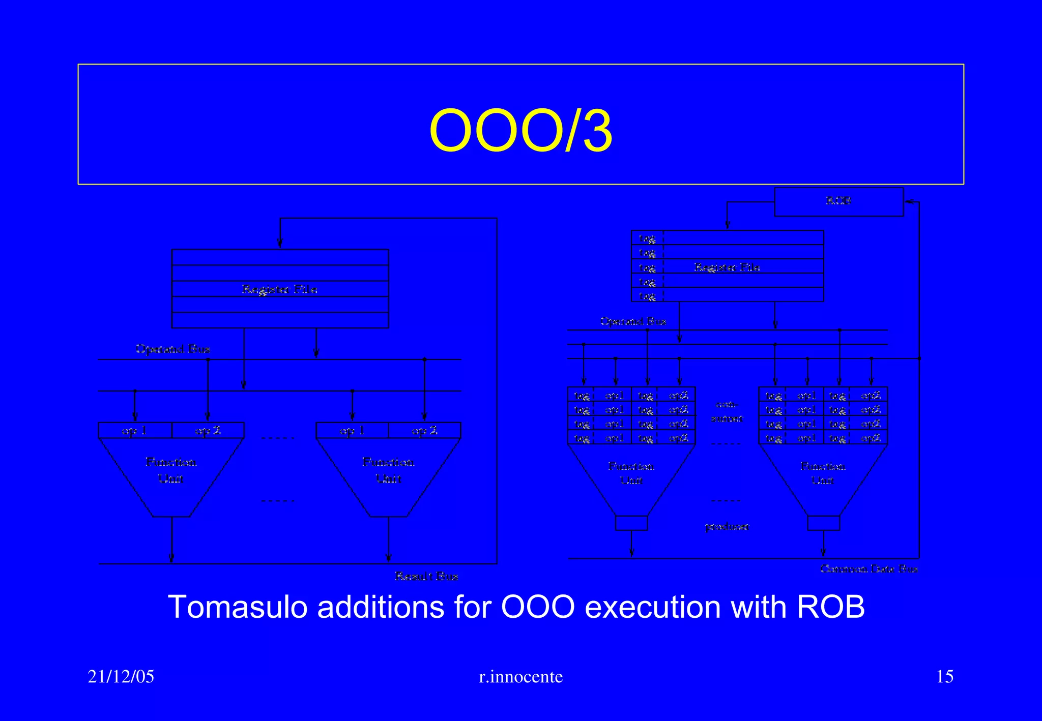
![21/12/05 r.innocente 76
Intel Itanium/3
• A typical Itanium instruction is a 3 operand
instruction designated with this syntax :
– [(qp)]mnemonic[.comp1][.comp2] dsts = srcs
• Examples :
– Simple instruction : add r1 = r2,r3
– Predicated instruction:(p5)add r3 = r4,r5
– Completer: cmp.eq p4 = r2,r3](https://image.slidesharecdn.com/ghan-nn-revised-160623091727/75/Nodes-and-Networks-for-HPC-computing-76-2048.jpg)