Download to read offline
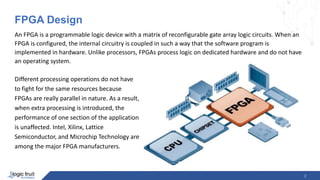

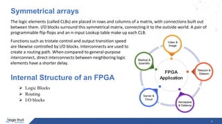

The document provides an overview of FPGA (Field-Programmable Gate Array) design, architecture, and applications, highlighting its programmable logic device nature and distinct internal circuitry that processes logic independently of an operating system. Major FPGA manufacturers like Intel and Xilinx are mentioned, alongside key architectural elements such as logic blocks, programmable interconnects, and memory. The document also emphasizes the advantages of parallel processing and pipelining in FPGA applications.


![Camera Sensor Technologies – An Overview [2023]](https://cdn.slidesharecdn.com/ss_thumbnails/camerasensortechnologiesanoverview2023-230222061349-06402e93-thumbnail.jpg?width=640&height=640&fit=bounds)