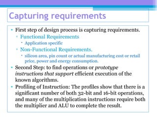
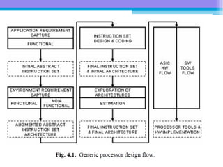
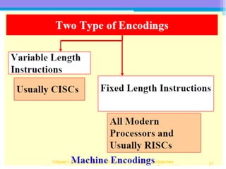
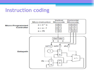
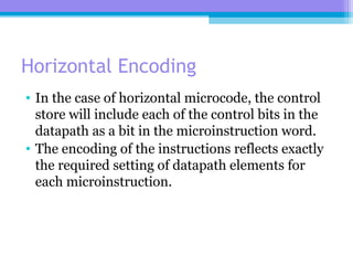
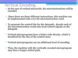
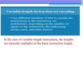
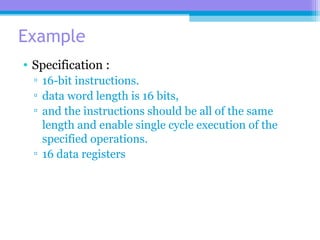
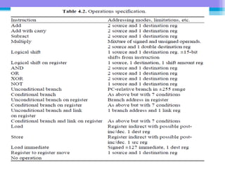
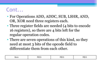
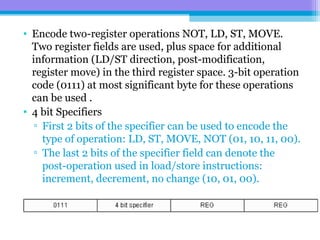
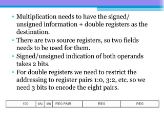
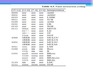
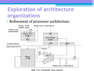
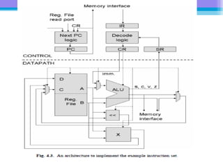
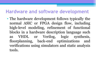
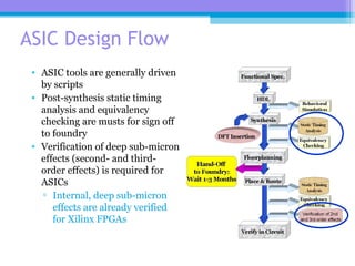
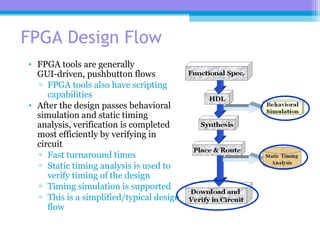
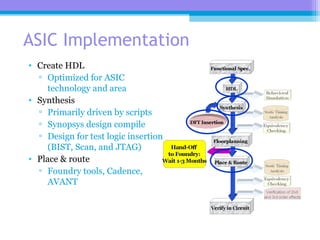
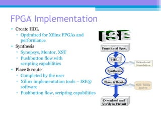
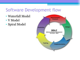
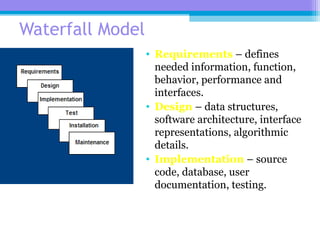
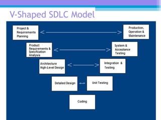
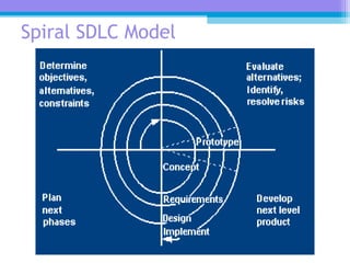
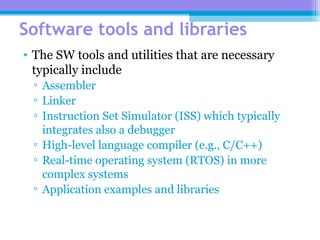
Module III:
Processor Design Flow and Memory :
Processor Design Flow :
Capturing requirements, Instruction coding, Exploration
of architecture organizations, hardware and software
development. Extreme CISC and extreme RISC, Very long
instruction word (VLIW).
Memory : Organization, Memory segmentation,
Multithreading, Symmetric multiprocessing.
Module III: A: Processor
Design flow
Capturing requirements
• First step of design process is capturing requirements.
▫ Functional Requirements
 Application specific
▫ Non-Functional Requirements.
 silicon area, pin count or actual manufacturing cost or retail
price, power and energy consumption.
• Second Step: to find operations or prototype
instructions that support efficient execution of the
known algorithms.
• Profiling of Instruction: The profiles show that there is a
significant number of both 32-bit and 16-bit operations,
and many of the multiplication instructions require both
the multiplier and ALU to complete the result.
Instruction coding
• To design the actual instruction set and its encoding to
form binary instructions.
• Maximal utilization of parallelism would require to
basically represent all the processor control signals in the
instruction word.
• To encode the operation and its operands in as few bits
as possible.
• The encoding is typically something between these
horizontal and vertical code approaches.
Cont..
• One goal is the low hardware complexity in
instruction decoder with easy assembling.
Instruction coding
• In the case of horizontal microcode, the control
store will include each of the control bits in the
datapath as a bit in the microinstruction word.
• The encoding of the instructions reflects exactly
the required setting of datapath elements for
each microinstruction.
Horizontal Encoding
• In the case of vertical microcode, the microinstructions will be
encoded.
• Since there are three different instructions, this machine can
be implemented with a two bit microinstruction word.
• To generate the control bits for the datapath, decode each of
the microinstruction words into local control signals on the
datapath.
• Vertical microprograms have a better code density, which is
beneficial for the size of the control store.
• Vertical microprograms use an additional level of encoding
• Thus, the machine with the vertically encoded microprogram
may have a longer critical path.
Vertical Encoding.
In the case of variable-length instructions, the lengths
are typically multiples of the basic instruction length.
Example
• Specification :
▫ 16-bit instructions.
▫ data word length is 16 bits,
▫ and the instructions should be all of the same
length and enable single cycle execution of the
specified operations.
▫ 16 data registers
Cont...
• For Operations ADD, ADDC, SUB, LSHR, AND,
OR, XOR need three registers each.
• Three register fields are needed (4 bits to encode
16 registers), so there are 4 bits left for the
regular operation codes.
• There are seven operations of this kind, so they
need at most 3 bits of the opcode field to
differentiate them from each other.
• Encode two-register operations NOT, LD, ST, MOVE.
Two register fields are used, plus space for additional
information (LD/ST direction, post-modification,
register move) in the third register space. 3-bit operation
code (0111) at most significant byte for these operations
can be used .
• 4 bit Specifiers
▫ First 2 bits of the specifier can be used to encode the
type of operation: LD, ST, MOVE, NOT (01, 10, 11, 00).
▫ The last 2 bits of the specifier field can denote the
post-operation used in load/store instructions:
increment, decrement, no change (10, 01, 00).
• Multiplication needs to have the signed/
unsigned information + double registers as the
destination.
• There are two source registers, so two fields
needs to be used for them.
• Signed/unsigned indication of both operands
takes 2 bits.
• For double registers we need to restrict the
addressing to register pairs 1:0, 3:2, etc. so we
need 3 bits to encode the eight pairs.
Exploration of architecture
organizations
• Refinement of processor architecture.
Extension for compatibility of instruction set
• The register file has now another write port D for
extended write-back of double-length
multiplication products.
• The multiplier and shifter are shown as separate
blocks from the basic ALU which only contains
add, subtract and logic functions.
Extension for compatibility of instruction set
• The shown setup implements a three-stage
pipelined processor (fetch–decode–execute)
which could be pipelined further as necessary by
adding pipeline registers to the datapath and
corresponding pipeline control, possibly with
forwarding logic control.
Hardware and software development
• The hardware development follows typically the
normal ASIC or FPGA design flow, including
high-level modeling, refinement of functional
blocks in a hardware description language such
as VHDL or Verilog, logic synthesis,
floorplanning, back-end optimizations and
verifications using simulators and static analysis
tools.
ASIC Design Flow
• ASIC tools are generally driven
by scripts
• Post-synthesis static timing
analysis and equivalency
checking are musts for sign off
to foundry
• Verification of deep sub-micron
effects (second- and third-
order effects) is required for
ASICs
▫ Internal, deep sub-micron
effects are already verified
for Xilinx FPGAs
FPGA Design Flow
• FPGA tools are generally
GUI-driven, pushbutton flows
▫ FPGA tools also have scripting
capabilities
• After the design passes behavioral
simulation and static timing
analysis, verification is completed
most efficiently by verifying in
circuit
▫ Fast turnaround times
▫ Static timing analysis is used to
verify timing of the design
▫ Timing simulation is supported
▫ This is a simplified/typical design
flow
ASIC Implementation
• Create HDL
▫ Optimized for ASIC
technology and area
• Synthesis
▫ Primarily driven by scripts
▫ Synopsys design compile
▫ Design for test logic insertion
(BIST, Scan, and JTAG)
• Place & route
▫ Foundry tools, Cadence,
AVANT
FPGA Implementation
• Create HDL
▫ Optimized for Xilinx FPGAs and
performance
• Synthesis
▫ Synopsys, Mentor, XST
▫ Pushbutton flow with
scripting capabilities
• Place & route
▫ Completed by the user
▫ Xilinx implementation tools – ISE®
software
▫ Pushbutton flow, scripting capabilities
Software Development flow
• Waterfall Model
• V Model
• Spiral Model
Waterfall Model
• Requirements – defines
needed information, function,
behavior, performance and
interfaces.
• Design – data structures,
software architecture, interface
representations, algorithmic
details.
• Implementation – source
code, database, user
documentation, testing.
V-Shaped SDLC Model
Spiral SDLC Model
Software tools and libraries
• The SW tools and utilities that are necessary
typically include
▫ Assembler
▫ Linker
▫ Instruction Set Simulator (ISS) which typically
integrates also a debugger
▫ High-level language compiler (e.g., C/C++)
▫ Real-time operating system (RTOS) in more
complex systems
▫ Application examples and libraries

Processor Design Flow architecture design

  • 1.
    Module III: Processor DesignFlow and Memory : Processor Design Flow : Capturing requirements, Instruction coding, Exploration of architecture organizations, hardware and software development. Extreme CISC and extreme RISC, Very long instruction word (VLIW). Memory : Organization, Memory segmentation, Multithreading, Symmetric multiprocessing.
  • 2.
    Module III: A:Processor Design flow
  • 3.
    Capturing requirements • Firststep of design process is capturing requirements. ▫ Functional Requirements  Application specific ▫ Non-Functional Requirements.  silicon area, pin count or actual manufacturing cost or retail price, power and energy consumption. • Second Step: to find operations or prototype instructions that support efficient execution of the known algorithms. • Profiling of Instruction: The profiles show that there is a significant number of both 32-bit and 16-bit operations, and many of the multiplication instructions require both the multiplier and ALU to complete the result.
  • 5.
    Instruction coding • Todesign the actual instruction set and its encoding to form binary instructions. • Maximal utilization of parallelism would require to basically represent all the processor control signals in the instruction word. • To encode the operation and its operands in as few bits as possible. • The encoding is typically something between these horizontal and vertical code approaches.
  • 6.
    Cont.. • One goalis the low hardware complexity in instruction decoder with easy assembling.
  • 8.
  • 9.
    • In thecase of horizontal microcode, the control store will include each of the control bits in the datapath as a bit in the microinstruction word. • The encoding of the instructions reflects exactly the required setting of datapath elements for each microinstruction. Horizontal Encoding
  • 10.
    • In thecase of vertical microcode, the microinstructions will be encoded. • Since there are three different instructions, this machine can be implemented with a two bit microinstruction word. • To generate the control bits for the datapath, decode each of the microinstruction words into local control signals on the datapath. • Vertical microprograms have a better code density, which is beneficial for the size of the control store. • Vertical microprograms use an additional level of encoding • Thus, the machine with the vertically encoded microprogram may have a longer critical path. Vertical Encoding.
  • 11.
    In the caseof variable-length instructions, the lengths are typically multiples of the basic instruction length.
  • 12.
    Example • Specification : ▫16-bit instructions. ▫ data word length is 16 bits, ▫ and the instructions should be all of the same length and enable single cycle execution of the specified operations. ▫ 16 data registers
  • 14.
    Cont... • For OperationsADD, ADDC, SUB, LSHR, AND, OR, XOR need three registers each. • Three register fields are needed (4 bits to encode 16 registers), so there are 4 bits left for the regular operation codes. • There are seven operations of this kind, so they need at most 3 bits of the opcode field to differentiate them from each other.
  • 15.
    • Encode two-registeroperations NOT, LD, ST, MOVE. Two register fields are used, plus space for additional information (LD/ST direction, post-modification, register move) in the third register space. 3-bit operation code (0111) at most significant byte for these operations can be used . • 4 bit Specifiers ▫ First 2 bits of the specifier can be used to encode the type of operation: LD, ST, MOVE, NOT (01, 10, 11, 00). ▫ The last 2 bits of the specifier field can denote the post-operation used in load/store instructions: increment, decrement, no change (10, 01, 00).
  • 16.
    • Multiplication needsto have the signed/ unsigned information + double registers as the destination. • There are two source registers, so two fields needs to be used for them. • Signed/unsigned indication of both operands takes 2 bits. • For double registers we need to restrict the addressing to register pairs 1:0, 3:2, etc. so we need 3 bits to encode the eight pairs.
  • 18.
    Exploration of architecture organizations •Refinement of processor architecture.
  • 19.
    Extension for compatibilityof instruction set • The register file has now another write port D for extended write-back of double-length multiplication products. • The multiplier and shifter are shown as separate blocks from the basic ALU which only contains add, subtract and logic functions.
  • 20.
    Extension for compatibilityof instruction set • The shown setup implements a three-stage pipelined processor (fetch–decode–execute) which could be pipelined further as necessary by adding pipeline registers to the datapath and corresponding pipeline control, possibly with forwarding logic control.
  • 22.
    Hardware and softwaredevelopment • The hardware development follows typically the normal ASIC or FPGA design flow, including high-level modeling, refinement of functional blocks in a hardware description language such as VHDL or Verilog, logic synthesis, floorplanning, back-end optimizations and verifications using simulators and static analysis tools.
  • 23.
    ASIC Design Flow •ASIC tools are generally driven by scripts • Post-synthesis static timing analysis and equivalency checking are musts for sign off to foundry • Verification of deep sub-micron effects (second- and third- order effects) is required for ASICs ▫ Internal, deep sub-micron effects are already verified for Xilinx FPGAs
  • 24.
    FPGA Design Flow •FPGA tools are generally GUI-driven, pushbutton flows ▫ FPGA tools also have scripting capabilities • After the design passes behavioral simulation and static timing analysis, verification is completed most efficiently by verifying in circuit ▫ Fast turnaround times ▫ Static timing analysis is used to verify timing of the design ▫ Timing simulation is supported ▫ This is a simplified/typical design flow
  • 25.
    ASIC Implementation • CreateHDL ▫ Optimized for ASIC technology and area • Synthesis ▫ Primarily driven by scripts ▫ Synopsys design compile ▫ Design for test logic insertion (BIST, Scan, and JTAG) • Place & route ▫ Foundry tools, Cadence, AVANT
  • 26.
    FPGA Implementation • CreateHDL ▫ Optimized for Xilinx FPGAs and performance • Synthesis ▫ Synopsys, Mentor, XST ▫ Pushbutton flow with scripting capabilities • Place & route ▫ Completed by the user ▫ Xilinx implementation tools – ISE® software ▫ Pushbutton flow, scripting capabilities
  • 27.
    Software Development flow •Waterfall Model • V Model • Spiral Model
  • 28.
    Waterfall Model • Requirements– defines needed information, function, behavior, performance and interfaces. • Design – data structures, software architecture, interface representations, algorithmic details. • Implementation – source code, database, user documentation, testing.
  • 29.
  • 30.
  • 31.
    Software tools andlibraries • The SW tools and utilities that are necessary typically include ▫ Assembler ▫ Linker ▫ Instruction Set Simulator (ISS) which typically integrates also a debugger ▫ High-level language compiler (e.g., C/C++) ▫ Real-time operating system (RTOS) in more complex systems ▫ Application examples and libraries

Editor's Notes

  • #23 The ISE Design Suite does support running from scripts, however, not all the utilities support this. The Implementation process (place and route) supports scripting.
  • #24 With an FPGA there is no time spent to complete an equivalency check or to have the device made at a foundry. This save months of development time. Static Timing Analysis is supported with the Xilinx Timing Analyzer which provides worst-case timing delay reporting. Typical FPGA designers spend most of this time determining why their timing constraints failed. This is usually resolved with making design changes. Some users do complete a timing simulation, but the more experienced designers (that have experience building FPGA designs) generally only check certain system transitions. Most FPGA customers spend 80% of their simulation time doing behavioral, and 20% doing timing simulation.
  • #25 Design for test includes: ATPG - Automatic Test Pattern Generation: Test vectors generated and run through the circuitry to test the part. BIST - Built-In Self Test: Used to test functionality of memory resources (specifically RAM) Scan - Internal Scan chain: Creates an internal shift register to test the functionality of the part.
  • #26 ISE Design Suite (Integrated Synthesis Environment). The ISE software tools encompass the entire flow. XST: Xilinx Synthesis Technology is a synthesis tool provided with the ISE software. Synopsys and Mentor are the primary 3rd party synthesis tool vendors that support the FPGA industry. Synopsys now includes Synplify synthesis.