Ennaoui cours rabat part ii
•
3 likes•3,667 views

Prof. Dr. Ahmed Ennaoui Photovoltaic Solar Energy Conversion Advanced course 2 ENIM Rabat Morocco إنتاج الكهرباء من الطاقة الشمسية

Recommended
Recommended
More Related Content
What's hot
What's hot (20)
Similar to Ennaoui cours rabat part ii
Similar to Ennaoui cours rabat part ii (20)
More from Prof. Dr. Ahmed Ennaoui
Ennaoui cours rabat part ii
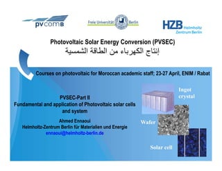
- 1. Photovoltaic Solar Energy Conversion (PVSEC) إﻧﺘﺎج اﻟﻜﻬﺮﺑﺎء ﻣﻦ اﻟﻄﺎﻗﺔ اﻟﺸﻤﺴﻴﺔ ﻴ ا إ ج ا ﻬﺮﺑ ء ﻦ ا Courses on photovoltaic for Moroccan academic staff; 23-27 April, ENIM / Rabat 23 27 Ingot PVSEC-Part PVSEC P t II crystal Fundamental and application of Photovoltaic solar cells and system Ahmed Ennaoui Wafer Helmholtz-Zentrum Berlin für Materialien und Energie ennaoui@helmholtz-berlin.de Solar cell
- 2. Highlight:Photovoltaic Solar Energy Conversion (PVSEC) Highlights Basic of solar cells and Modules Light absorption and band to band transition g p Quantum efficiency and absorption coefficient Generation and recombination processes Shockley-Read Hall Recombination (SRH) Continuity equation and Transport process Silicon to binary and ternary compounds From silicon solar cell as example of PN j ti F ili l ll l f junction Performance of solar cells Equivalent Circuit model: series (Rs) and shunt resistance (Rsh) Change in cell performance with Rs and Rsh Change in short circuit current and open-circuit with solar radiation Change in short circuit current and open-circuit with the temperature open circuit Performance measurement standard conditions Prof. Ahmed Ennaoui / Helmholtz-Zentrum Berlin für Materialien und Energie
- 3. Basic of solar cells and Modules Sun has roughly T = 5800 K Solar cell has roughly T = 300 K Two basic functions of a solar cell 1. 1 Light absorption: generation of free excess charge carriers photocurrent, I Power 2. Charge separation: separate/extraction of excess electrons and holes IxV p photovoltage, V g , Conversion of the Sun light in the „Black Box“ • To absorb the solar spectrum as efficient as possible • To collect photogenerated charge carriers • Charge transport must be possible • To make electron go to one side and holes to another current flow Ahmed Ennaoui / Helmholtz-Zentrum Berlin für Materialien und Energie
- 4. Basic: Task of Photovoltaic Key aim is to g y generate electricity from solar spectrum y p Power = Voltage x Current J [A/cm ] 2 . J xV . (J ,V ) m m [Watt/cm2] [Volt ] [A/cm2] Jm m m Two challenges Generating a large current. V [Volt ] Generating a large voltage. Vm High current. High voltage But low voltage But low current E Excess energy l t t h t lost to heat Sub-band gap light is lost Ahmed Ennaoui / Helmholtz-Zentrum Berlin für Materialien und Energie
- 5. Basic: Absorption-Separation-Collection Photons absorbed Electron flow Electrical current Photon flux gives number of photons/unit time/unit area/wavelength Φ(λ) = Φ 0 .exp(−α λ x) ⎯R(λ )→ ⎯⎯ Φ(λ) = Φ 0 (λ).(1 − R λ ).exp(−α λ x) Electrons collected dΦ Load G(x) = − = αΦe−αx dx dp J = σE Dp dx ceptor P = Voltage x Current Voltage Δ = μe – μh μe V lt Δμ Acc μ = chemical potential Rec Voc or μh Dono 0 W Ln La= 1/α Ahmed Ennaoui / Helmholtz-Zentrum Berlin für Materialien und Energie
- 6. Basic: Quantum efficiency • Photoccurrent = how much light converted? This ratio can be measured Maximum short circuit current Electrons collected / Photons absorbed • Limited information on the electronic properties • Information on the optical properties of the device electrons N out = J A/cm 2 [ ] e[Coulomb] hc 1239 hν = ⇒ EG (eV ) = λ λ (nm) N photons = [ Φ Watt/cm 2 ] hν [Joule ] in Load L d External Quantum Efficiency, EQE cceptor dp J = σE D p N electron 1 J ( λ ) hc dx EQE = photons = Q out N in Φ (λ ) e λ Ac → → ∇p μe E Internal Quantum Efficiency EQE Rec R Voc IQE = 1 − R (λ ) μh Origine of the photovoltage or Chemical potential Dono x=0 La= 1/α x=W x = Ln EF,n = μe EF,h = μh Ahmed Ennaoui / Helmholtz-Zentrum Berlin für Materialien und Energie
- 7. Basic: Quantum efficiency measurements current/charge of 1 electron External Quantum Efficiency" EQE" = EQE Total power of photon/energy of 1 photon Beam splitter Monochromator Chopper equipped with more gratings* EQE vs. λ EG *Gratings should have line density as high as possible for achieving high resolution and high power throughput. (600 – 3000 lines/mm). 1 - Reference measurement 2 – Cell Measurement 3 – Final Result J sc = q.EQE REF .Φ1 REF J sc = q.EQECELL .Φ2 CELL CELL MON,1 J sc J sc EQE CELL = MON,2 . REF EQE REF J MON,1 sc = q.EQE q Q MON .aΦ 1 J MON,2 sc = q.EQE q Q MON .aΦ 2 J sc J sc MON,1 CELL J sc J sc EQE MON .a = EQECELL .a = MON,2 .EQEMON .a qΦ 1 J sc Ahmed Ennaoui / Helmholtz-Zentrum Berlin für Materialien und Energie
- 8. Basic: EQE and and absorption coefficient ( ) E(k) p Photon absorption in a direct band-gap e.g. GaAs Conduction Band semiconductor B α= (h ν − E G ) 2 EC hν 1 Direct Bandgap Eg EV Photon (α .h ν )2 vs. (hν − E G ) → E G Valence Band Cut-off λ vs. EG 1.24 -k +k λ G [μm] = E G [eV] J sc = q ∫ Φ (λ ) EQE (λ ) dλ E(k) λ e.g. Si Conduction Photon absorption in an Band indirect band-gap semiconductor 1 EG+Ep Phonon EC A Eg α = (hν − EG ) 2 Photon EV hν Valence Ep (α .h ν )2 vs. (h ν − E G ) → E G Band -k +k Ahmed Ennaoui / Helmholtz-Zentrum Berlin für Materialien und Energie
- 9. Basic: absorption coefficient and absorption length Light absorption E G (T) = E g (0) − A.f(T) Si Ge GaAs EG (eV) 1 12 1.12 0.66 0 66 1.42 1 42 Temperature changes: EG ↑ as T ↓, Changing the absorption edge Absorption ↔ Generation hν Φ = Φ0 .(1 − R λ ).e−αx 1 Φ Φ0(E) α λ = − . ln d Φ0 .(1 − R λ ) ΦA(E) Φt(x) dΦ G(E, x) = − = Φ o (E).(1 - R).α). -αx dx Φ0 = ΦR + ΦA + ΦT Depth x Φ Surface x =1/α Φr(E) 100% = R λ + A λ + Tλ Ahmed Ennaoui / Helmholtz-Zentrum Berlin für Materialien und Energie
- 10. Basic: absorption coefficient and absorption length 100 nm Ahmed Ennaoui / Helmholtz-Zentrum Berlin für Materialien und Energie
- 11. Basic: improuvement, Light traping Influence of the layer thickness on the photocurrent of Si Realization: • Etching and texturing of semiconductors. • Implementation of particles for scattering deposition on rough or structured surfaces d ii h d f Ahmed Ennaoui / Helmholtz-Zentrum Berlin für Materialien und Energie
- 12. Basic: Challenging parameters Important cost factor All device parameters Reflection Loss Material parameter € J sc = q . ∫ [η(λ) . (1 − R λ ).Φ 0 (λ ) . exp - α λ .d ]dλ η( ) ( ) p EG Decisive Material parameter Light trapping η(λ) =↑ % EQE or η or IPCE - incident photon to electron conversion efficiency) p y) 1 J ph hc EQE = . Φ(λ) q λ Resistive loss Reflection loss Top contact “loss” loss Recombination loss Back contact „Loss“ Ahmed Ennaoui / Helmholtz-Zentrum Berlin für Materialien und Energie
- 13. Basic: Close look to EQE 1 J ph (λ ) hc η(λ) = EQE = . Φ(λ) q λ (2) Losses due to reflection (3) Losses due to rear surface and low diffusion length passivation and reduced absorption at long wavelengths and low diffusion length (4) Complete loss due to missing absorption (1) Losses due to front surface recombination and absorption Wavelength at 1.24 λ G [μm] = in passivation and antirection the band gap E G [eV] coating layers Ahmed Ennaoui / Helmholtz-Zentrum Berlin für Materialien und Energie
- 14. Basic: PN junction Loss in Jph Good surface passivation. Texturing in the form of pyramids so that Antireflection coatings. light is trapped at the surface (<60nm) Low metal coverage of the top surface. Light trapping or thick material (but not thicker than diffusion length). High diffusion length in the material. Junction depth optimized for absorption in emitter and base. Low reflection by texturing Resistive loss Reflection loss Top contact “loss” “l ” Recombination loss Back contact „Loss“
- 15. Generation vs. recombination processes Generation (g) requires an input of energy given to an electron: gy g - Phonons - vibrational energy of the lattice - Photons - Light, or electromagnetic waves - Kinetic energy from another carrier (Impact ionization ) Electron El t EC thermalizes Generation to band edge Ekin K.E. = E − EC EV EC Generation energy > EG Ekin energy = EG energy < EG EV - Impact ionization The electron hits an atom, and break a covalent bond to generate an electron-hole pair, if the kinetic energy is larger than the energy needed to t generate th pair. Th process continues with th newly generated t the i The ti ith the l t d electrons, leading to avalanche generation (e-h). Ahmed Ennaoui / Helmholtz-Zentrum Berlin für Materialien und Energie
- 16. Generation vs. recombination processes Recombination (r) is the opposite of generation, leading to voltage and current loss. Non-radiative recombination phonons, lattice vibrations. Radiative recombination photons (dominating in a direct bandgap materials ) Auger recombination charge carrier may give its energy to the other carrier. Recombination processes are characterized b th minority carrier lif ti τ. R bi ti h t i d by the i it i lifetime Equilibrium: charge distributions np = ni2 Out of equilibrium: The system tries to restore itself towards equilibrium through R-G Steady-state rates: deviation from equilibrium y q r = B .pn ⎫ ( ⎬ R = r − g = B pn − ni 2 ) B(Si) = 2 × 10 −15 cm 3 /s g = B.p0 n0 = Bni2 ⎭ Electron thermalizes to band edge bination xcess energy given rrier in EC EC y th same band d EC Auger recomb to another car Radiative Non-radiative E(eV) recombination recombination Phonon he Ex o A EV EV EV Ahmed Ennaoui / Helmholtz-Zentrum Berlin für Materialien und Energie
- 17. Shockley-Read Hall Recombination (SRH) The impurities create deep-level-traps (ET) within the bad gap The electron in transition between bands passes through ET EC (1)+(3): one electron reduced from Conduction band (1) (2) and one‐hole reduced from valence‐band and ET (2)+(4): one hole created in valence band and (3) (4) one electron created in conduction band EV Steady state Steady-state rates: R = A (np-ni2) = deviation from equilibrium: (np n n, p and NT inside Δx are held constant by the balancing effect of distinct different process np − n i2 R= ⎛ 1 ⎞ ⎛ ⎞ ⎜ ⎟(n + n1) + ⎜ 1 ⎟(p + p1) cp,n: capture coefficient of the recombination process ⎜c N ⎟ ⎜c N ⎟ 1⎝ p T ⎠ ⎝ n T⎠ NT: density of the recombination levels. τp = ↑ 1 ↑ τn = σn,p: capture cross sections for e and h. σ p v t ,h N T σ n v t ,n NT ET: energy levels inside the energy gap. ( ET −Ei ) − ( E T −Ei ) vth: average thermal velocity of e and h. pT, nT: number of empty states available n1 = n i e k BT p1 = n i e k BT n, p: number of electrons or holes n1 , p1: number of electrons and holes at ET Low level i j ti L l l injection Δn Δp n - type material R SRH = p − type material R SRH = τn τp Ahmed Ennaoui / Helmholtz-Zentrum Berlin für Materialien und Energie
- 18. Summary: Generation & Recombination Auger recombination (dominant effect at high carrier concentration) Ekin= -qELsc q EC Direct Loss to thermal Shockley-Read Hall recombination vibrations Ekin recombination direct band EV Impact ionization is a generation mechanism. ⎛ 1 1 1 ⎞ When the electron hits an R = RSRH + RDirect + RAuger = Δn⎜ + + ⎟ atom, it may break a ⎜τ ⎟ ⎝ SRH τ Direct τ Auger ⎠ covalent bond to generate ( = Δn cn NT + BN D + cn,Auger .N D 2 ) an electron-hole pair. ( ⇒ τ eff = cn NT + BN D + cn,Auger .N N D ) 2 −1 The process continues with the newly generated electrons leading to avalanche electrons, generation of electrons and holes. τ : average time it takes an excess minority carrier to recombine (1 ns to 1 ms) in Si τ τ : depends on the density of metallic impurities and the density t/teff of crystalline defects. Ahmed Ennaoui / Helmholtz-Zentrum Berlin für Materialien und Energie
- 19. What we have learned? Photo absorption and photo generation, Direct and indirect band gap, EQE, IQE absorption coefficient, absorption length, excess minority carrier , carrier lifetime Recombination: Non Radiative, Radiative, Auger Shockley-Read Hall Recombination (dominant process in Si) There are wide variety of generation‐recombination events that allow restoration of equilibrium once the stimulus is removed. Direct recombination is photon‐assisted, indirect recombination phonon assisted. Recombination lifetime in Si is controlled by Auger recombination at high carrier concentration Recombination life time in Si is controlled by SRH at low carrier densities and depends on the amount of impurities and defects. http://en.wikipedia.org/wiki/Main_Page Ahmed Ennaoui / Helmholtz-Zentrum Berlin für Materialien und Energie
- 20. Basic: Continuity equation and Transport process Continuity equation for minority carriers: y q y ∂ ( A . Δx . n ) A . J n (x) - A . J n (x + dx) = + A . g n . Δx − A . rn . Δx ∂t −q Φ = Φ0 .(1 − Rλ ).exp(−αx) Light flux ∂n J n (x) - J n (x + dx) 1 = + g n − rn = ∇.J n + g n − rn ∂t − q.Δx q ∂ ∇ ⋅ (∇ × H ) = ∇ ⋅ J cond + ∇⋅D = 0 ∂t ( ) ∇ ⋅ Jn + J p + ∂ρ ∂t = 0, ρ = q( p − n + N D − N A ) Maxwell ⎧ ∂n = 1 ∇ ⋅ J + G − R ⎪ ∂t q n n n ⇒ ⎨ ∂p 1 ⎪ = − ∇ ⋅ J p + Gp − Rp ⎩ ∂t q Ahmed Ennaoui / Helmholtz-Zentrum Berlin für Materialien und Energie
- 21. Basic: Continuity equation and Transport process rain Evaporation p In flow Rate of Out flow dn increase of = (in flow – out flow) + Rain - Evaporation water level t l l dt 1 in lake = ∇ .J n + gn - rn q ∂n 1 ∂p 1 = ∇ .J n + g n - rn = ∇ .J p + g p - r p ∂t q ∂t q J n = qnμn E + qDn∇ n J p = qnμ p E + qD p ∇ p Ahmed Ennaoui / Helmholtz-Zentrum Berlin für Materialien und Energie
- 22. Basic: Continuity equation and Transport process Carriers are collected when they are: Generated closer t th j ti G t d l to the junction Generated within a diffusion length of the junction ∂n =0 Key parameters for high collection are: ∂t Minority carrier diffusion y Surface recombination Difficult to achieve high collection near front surface and also rear Differential equation is simple only when G = constant. d 2 Δn Δn G(λ( x) d 2 Δp Δp G(λ( x) 2 = 2 − 2 = 2 − dx Ln Dn dx Lp Dp −x +x Δn(x) = Aexp + Bexp + Gτ n ← Bondary conditions Ln Ln Acceptor p(-αx) ΕF,n=μe Donor ΕF,p=μh Φ= 0(1-R)exp D A Acceptor Rec Rec Voc =Φ or ΕF,p=μh A ΕF,n=μe Dono La= 1/α Lp W 0 0 W Ln La= 1/α Ahmed Ennaoui / Helmholtz-Zentrum Berlin für Materialien und Energie
- 23. Basic Diode J-V equation dΔp n Applying the same boundary conditions as in the ideal diode case case. J p = qD p dx Differentiating to find the current dΔn p Equating the currents on the n-type and p-type sides, we get: J n = qD n dx ⎛ Dn Dp ⎞ J= ⎜q n p,0 + q p n,0 V ⎟ (exp qV − 1) − qG(L + L + W) ⎜ L Lp ⎟ k BT n p ⎝ n ⎠ J0 Photocurre nt J L - JL + JD ⎛ qV ⎞ J = J 0 ⎜ exp n.k B T − 1⎟ − J L ⎜ ⎟ ⎝ 1 4 42 4 43 ⎠ Dark current, J D J0 : saturation current kB : Boltzmann`s constant, 1.381 10-23 J/Kelvin n : ideality factor ⎡ D n n i2 D p n i2 ⎤ J0 = q⎢ + ⎥ ni: carrier concentration ⎢ Ln N A L p N D ⎣ ⎥ ⎦ NA,ND. Doping concentration Ahmed Ennaoui / Helmholtz-Zentrum Berlin für Materialien und Energie
- 24. Silicon (Diamond) to Chalcopyrite (Tetragonal) Diamond structure IV nq N + mqM Grimm Sommerfeld rulea Grimm-Sommerfeld-rulea =4 Si n + m + ... N,M elements, n,m atoms/unit cell and qN, qM valence electrons sp3 hybrid bonds III-V zincblende structure II-VI Epitaxial film: Polycrystalline thin film: GaAs , InP… CdTe, ZnS II-IV-V2 I-III-VI2 Epitaxial film: Polycrystalline thin film: ZnGeAs, … Cu(In,Ga)(Se,S)2 (Chalcopyrite and related compounds) I-III-VI2 Alloy: Group I= Cu, Group III= In and Ga, Group VI = Se and S Ahmed Ennaoui / Helmholtz-Zentrum Berlin für Materialien und Energie
- 25. Basic: how to make a solar cell: The p-n junction IB IIB IIIB IVB VB VIB Si Periodic Table 5 8 Ge 6 7 B C N O GaAs 13 14 15 16 Al Si P S CdTe 29 30 31 32 33 34 Cu Zn Ga Ge As Se I P InP 48 49 50 51 52 Cd In Sn Sb Te AlSb CIGS CZTS Metallurgical Junction NA ND - - - - - - + + + + + - - - - - - + + + + + P - - - - - - + + + + + N - - - - - - + + + + + Space ionized acceptors Charge Region ionized donors E-Field h+ diffusion = h+ drift e- diffusion = e- drift
- 26. Basic: PN junction at equilibrium ⎧p p0 ≈ N A ⎧ n no ≈ N D ⎪ ⎪ ⎨ n 2 ⎨ ni 2 ⎪n p0 ≈ i ⎪ p n0 ≈ ⎩ EC NA ⎩ ND n = p = ni qVbi n i = BT 3 e −EG 2 kT Ei EF EV 300K : n i ≅ 1.5 × 10 10 cm −3 ρ(x) W + qND Built-in voltage Vbi -qNA - N x qVb = ( Ei − E F ) p + ( E F − Ei )n bi V (x) nn0 = ni exp[( E F − Ei ) k BT ] Vbi p p 0 = ni exp[Ei − E F k BT ] p E(x) x ⎛ ⎞ k BT ⎜ p p 0 nn0 ⎟ ⎛ N AND ⎞ Vbi = ln ≈ VT ln⎜ ⎟ − xp xn q ⎜ n2 ⎟ ⎜ 2 ⎟ ⎝ i ⎠ ⎝ ni ⎠ Emax x A. Ennaoui / Helmholtz-Zentrum Berlin für Materialien und Energie
- 27. Basic: PN junction in the dark Depletion region width: Solve 1D Poisson equation using depletion charge approximation, subject to the following boundary conditions: V ( − x p ) = 0, V ( xn ) = Vbi , E (− xn ) = E ( x p ) = 0 p-side: V p ( x) = qN A 2k s ε 0 (x + x p )2 qN D n-side: Vn ( x) = − ( xn − x )2 + Vbi 2k s ε 0 Use the continuity of the two solutions at x=0, and charge neutrality, to obtain the expression for the depletion region width W: xn + x p = W ⎫ V p (0) = Vn (0) ⎪ → W = 2k s ε0 ( N A + N D )Vbi ⎬ ⎪ qN A N D N A x p = N D xn ⎭ A. Ennaoui / Helmholtz-Zentrum Berlin für Materialien und Energie
- 28. Basic: PN junction in the dark Depletion layer capacitance: Consider a p+n, or one-sided junction, for which: 2k s ε 0 (Vbi m V ) W= qN D The depletion layer capacitance is calculated using: dQc qN D dW qN D k s ε 0 1 2(Vbi m V ) C= = = → 2= 1 C2 dV dV 2(Vbi m V ) C qN D k s ε0 1 Measurement setup: slope ∝ ND W dW Reverse bias Forward bias vac ~ V Vbi − V V A. Ennaoui / Helmholtz-Zentrum Berlin für Materialien und Energie
- 29. Basic: PN junction in the dark Ideal Current-Voltage Characteristics: Assumptions: • Abrupt depletion layer approximation • Low level injection Low-level injected minority carrier density much smaller than the majority carrier density • No generation-recombination within the space-charge region (SCR) Depletion l D l ti layer: EC W n.p = n exp(V / VT ) 2 i qV p n (x n ) = n n0 exp(V/VT ) EF Fn E Fp EV n p ( −x p ) = n p0 exp(V/VT ) k BT − xp VT = xn q A. Ennaoui / Helmholtz-Zentrum Berlin für Materialien und Energie
- 30. Basic: PN junction in the dark Forward bias: Reverse bias: EC W Ln qV EC q(Vbi + V ) q(Vbi − V ) E Fp qV EV E Fn E Fn E Fp p EV Lp W Reverse saturation current is due to minority carriers being collected over a distance on the order of the diffusion length.
- 31. Basic: PN junction in the dark Quantitative p-n Diode Solution / Little MATH Q. neutral Region Q. neutral Region Depletion Region P-type N-type E≠0 E=0 E=0 -∞ -xp Electrical field +xn +∞ ∂Δn p d Δn p 2 Δn p ∂Δp n d 2 Δp n Δp n = Dn − + G L existe in the depletion = Dp − + GL ∂t dx 2 τn region the minority ∂t dx 2 τp d 2 Δn p Δn p carrier diffusion i diff i 0 = Dn − Does not apply here d 2 Δp n Δp n dx 2 τn 0 = Dp − dx 2 τp Boundary condition Boundary condition Boundary condition Boundary condition Δn p ( x → −∞) = 0 Δn p ( x → − x p ) = ? Δp n ( x → x n ) = ? Δp n ( x → +∞) = 0 n i2 ⎛ qV ⎞ n i2 ⎛ qV ⎞ Δn p (x = − x p ) = ⎜ exp ⎜ − 1⎟ ⎟ Δp n (x = x p ) = ⎜ exp ⎜ − 1⎟ ⎟ NA ⎝ k BT ⎠ ND ⎝ k BT ⎠
- 32. Basic: PN junction in the dark Total current density: y • Total current equals the sum of the minority carrier diffusion currents defined at the edges of the SCR: I tot = I diff ( n ) + I diff ( −x p ) p (x n ⎛ D p p n0 D n n p0 ⎞ V/V I D = qA ⎜ ⎜ L + Ln ⎟ ( ⎟ e T −1 ) ⎝ p ⎠ • Reverse saturation current density: I 0 = J 0 . A current Current density area V (volt) 2 2 ni p n0 ≈ ND n p0 ≈ ni NA ⎛ D p p n0 D n n p0 ⎞ ⎛ Dp Dn ⎞ I 0 = qA ⎜ + ⎟ = qAn i2 ⎜ + ⎟ ⎜ L Ln ⎟ ⎜L N ⎟ ⎝ p ⎠ ⎝ p D LnN A ⎠ A. Ennaoui / Helmholtz-Zentrum Berlin für Materialien und Energie
- 33. Basic: How to make a solar cell: Dark current + Dark current Φ(x) N P Photocurrent C Ph t t Current: t 2 Φe-αx • Diffusion courant (electron, region 1) 1 3 • Generation current in SCR (region 2) Ohmic xp xn Ohmic • Diffusion current (holes region3) contact E contact ⎛ ⎞ 1 3 qV 2 J = J 0 ⎜ exp − 1 ⎟ − J ph p-type n-type k BT ⎜ ⎟ ⎝ ⎠ W EC J ph = J p , diff ( x n ) + J G ( x n ) + J n , diff ( x p ) qV 1 2 3 E Fn E Fp EV − xp xn A. Ennaoui / Helmholtz-Zentrum Berlin für Materialien und Energie
- 34. Basic: PN junction under illumination (Space Charge Region, SCR) Φ(x) N P Generation current i space charge region 2 G ti t in h i 2 J G ,n = J G ,p Φe-αx 1 3 Continuity C ti it equation (for electron) ti (f l t ) ∂n 1 dJ n Δp n Ohmic xp xn = − + GL ∂t q dx τp contact E Ohmic 1 2 3 contact Steady-state p-type n-type xn 1 dJ n 0= + GL J G = q ∫ G(x)dx q dx xp W G(x) = Φαexp( αx) Φαexp(- J G ,n ( x n ) = qΦ e ( - αx p ) − e − αx n = qΦe − αx p (1 − e ) − αW A. Ennaoui / Helmholtz-Zentrum Berlin für Materialien und Energie
- 35. Basic: PN junction under illumination (diffusion current) Φ( ) (x) N P Neutral region 3 n type n-type Diffusion current: holes 2 dΔp Φe-αx J p ,dff . = qD p 1 3 dx −x / Lp + x / Lp Φατ p Δp = Ae + Be + xp xn 1 − α 2 L2p Ohmic Oh i E Ohmic Boundary conditions contact 1 3 contact 2 p-type n-type Δp = 0 x = x c → +∞ L p << d n ; 1 / α ⇒ B = 0 Δp = 0 x = x n ( E = 0) Φατ p −αx n + x n / L p ⇒A= e 1 - α Lp 2 2 Δp = Φατ p 1− α L 2 2 ( e − αx n e − α ( x − x n ) − e −( x − x n ) / L p ) p αL p J p ,diff . = −qΦ e − αx n 1 − αL A. Ennaoui / Helmholtz-Zentrum Berlin für Materialien und Energie
- 36. Basic: PN junction under illumination Neutral region 1 p type p-type Φ(x) N P 2 Diffusion current: electron Φe-αx dΔ dΔn 1 3 J n ,dff . = qD n dx x / Lp Φατ n Ohmic x´c xp xn xc Δn = Ae − x / L n + Be + 1 − α 2 L2n contact E Ohmic 1 3 contact 2 p-type n-type Boundary conditions x = x p Δn = 0 (electrical field E) x = x ´c → Δn(x ´c ) Δn(x ´c ) depends on surface recombination (S 0 ) ( p ( Surface recombination S0 ⎛ A n − xp /L n B n xp /L n Φα 2 τ n −αx p ⎞ J n,diff. ( x n ) = qD n ⎜ − ⎜ L e + e − e ⎟ ⎟ ⎝ n Ln 1 − α Ln 2 2 ⎠ A. Ennaoui / Helmholtz-Zentrum Berlin für Materialien und Energie
- 37. Basic: PN junction under illumination 1 For an efficient P - N junction d p << ⇒ J n,diff. ≈ 0 α ( ⎧J G ( x n = W ) = −qΦ 1 − e − αW ) ⎪ Origine at x p = 0 and x n = W ⎨ αL p ⎪ J p,diff. ( x n ) = −qΦ e − αW ⎩ 1 + α 2 L2p ⎛ 1 ⎞ J ph = −qΦ ⎜1 − e − αW ⎟ ⎜ 1 + αL ⎟ ⎝ p ⎠ 1 Maximum J ph M i f αW >> 1 (W >> ) → e.g. pin - j for i junction ti α A. Ennaoui / Helmholtz-Zentrum Berlin für Materialien und Energie
- 38. PN junction under illumination / Efficient p-n diode ⎛ 1 ⎞ ⎛ 1 ⎞ J ph = − qΦ ⎜1 − e − αW ⎟ Φ = Φ 0 (1− R ) ⎯⎯ ⎯ ⎯→ J ph = qΦ 0 (1 − R ) ⎜1 − e − αW ⎟ ⎜ 1 + αL ⎟ ⎜ 1 + αL ⎟ ⎝ p ⎠ ⎝ p ⎠ ⎛ 1 ⎞ A = cell area → I ph = J ph . A = AqΦ 0 (1 − R )⎜1 − e − αW ⎟ ⎜ ⎟ ⎝ 1 + αL p ⎠ Φ0 = Number of photon per unit area, per unit time, per wavelength increment incident power: Pinput = hν . Φ0 . A λ(nm) . EQE 1239 I ph AqΦ 0 (1 − R ) ⎛ ⎜1 − 1 ⎞ q ⎛ 1 ⎞ = e − αW ⎟ = . (1 − R ) ⎜1 − e − αW ⎟ Pinput hνΦ 0 .A ⎜ 1 + αL p ⎝ ⎟ hν ⎠ ⎜ 1 + αL ⎝ p ⎟ ⎠ Multimeter I ph geometry q ⎛ 1 ⎞ EQE = = (1 − R ) ⎜1 − e − αW ⎟ Piinput ⎜ 1 + αL ⎟ ⎝ p ⎠ Pyranometer hν reflexion Absorption Minority carrier 1 1 λ (nm) g diffusion length = = coefficient hν hc 1239 q qλ A. Ennaoui / Helmholtz-Zentrum Berlin für Materialien und Energie
- 39. Basic: PN junction Loss in Jph ⎛ 1 ⎞ η = (1 − R) ⎜ 1 − e −αW ⎟ ⎜ 1 + αL ⎟ ⎝ p ⎠ SEM image A. Ennaoui / Helmholtz-Zentrum Berlin für Materialien und Energie
- 40. Basic: Open circuit Voltage, VOC ⎡ q qV ⎤ nk B T ⎛ J L ⎞ J = J D + J ph = J 0 ⎢ exp − 1 ⎥ − J L = 0 ⇒ V OC = l ⎜ ln ⎜ + 1⎟ ⎟ ⎣ nk B T ⎦ q ⎝ J0 ⎠ J0 : saturation current , n : ideality factor, kB : Boltzmann ´s constant, VOC: open circuit voltage JL or Jph photocurrent voltage, h - JL + JD Open circuit voltage O i it lt nk B T ⎛ J L ⎞ V OC = ⎜ ln ⎜ + 1⎟ ⎟ q ⎝ J0 ⎠ A. Ennaoui / Helmholtz-Zentrum Berlin für Materialien und Energie
- 41. Open circuit Voltage, VOC For a given band gap EG, we need trade-offs trade offs nk B T ⎛ J L ⎞ ⎛ D n n i2 D p n i2 ⎞ V OC = ⎜ ln ⎜ + 1⎟ J0 = q ⎜ + ⎟ q J0 ⎟ ⎜L N Lp N D ⎟ ⎝ ⎠ ⎝ n A ⎠ Dp 1 Dn 1 qn i w E J 0 = [qN C N V ( + )+ ]exp - G Diffusion length τp ND τn NA τnτp k BT Doping Dn Dp kT = = VT = (VT = 300K = 25mV ) μn μp q VOC A. Ennaoui / Helmholtz-Zentrum Berlin für Materialien und Energie
- 42. Power output characteristics mpp = Maximum Power Point JSC.VOC.FF V FF Jmpp.Vmpp J Rmpp EFF.= PSun JSC.VOC P=I.V Fill Factor J mpp x Vmpp Pmpp= Impp x Vmpp J SC .VOC V Vmpp Jmpp . Vmpp EFF= PSun Inverse of slope Vmpp/Impp is characteristic resistance is characteristic resistance Jmpp mmp Jsc VOC Pmax A. Ennaoui / Helmholtz-Zentrum Berlin für Materialien und Energie
- 43. Importance of mobility μ and Diffusion length, Lp,n The higher mobility μ, the better is the carrier extraction g y L : Mean free length of path (L2 = D.τ) gives how long charge carrier (Lp or Ln) can travel in a volume of a crystall lattice before recombination takes place dn J n = qμ n nE + qD dx velocity v Mobility μ = = Field E A. Ennaoui / Helmholtz-Zentrum Berlin für Materialien und Energie
- 44. Dark current and photocurrent ⎡ qV ⎤ ⎛ qV D ⎞ ID = I 0 ⎢exp − 1⎥ I = I 0 ⎜ exp − 1⎟ - I L ⎣ nkT ⎦ ⎝ nkT ⎠ V (volt) V (volt) A. Ennaoui / Helmholtz-Zentrum Berlin für Materialien und Energie
- 45. Limitation of VOC by I0 and JSC At room temperature: VT = kBT/q = 26 mV VOC increases by 0.06 V if I0 decreases by one order of magnitude VOC increases by 0.06 V if ISC increases by one order of magnitude V (volt) V (volt) Diode saturation current density for nearly ideal Si solar cells I 0 (Si) ≈ 10 −13 A.cm −2 A. Ennaoui / Helmholtz-Zentrum Berlin für Materialien und Energie
- 46. Energy conversion efficiency of a solar cell Maximum Power Point = PMPP = V MP . I MP POWER IN MPP VOC . I SC EFFICIENCY = EFFICIENCY = POWER OF SUN LIGHT PSun V MP Optimal load resistance in the MPP R MPP = L Importance of the I MP solar cell efficiency EFFECIENCY ↑ W/cm2) ↓ I(A/cm2) x V(W MATERIAL + AREA m COST FOR PV ↓ €/Wp↓ V (volt) A. Ennaoui / Helmholtz-Zentrum Berlin für Materialien und Energie
- 47. One diode model / Equivalent Circuit Ideal diode (dark current , ID) JD J. RS (Voltage drop) (Shockley diode equation) J ⎡ qV D ⎤ J D = J 0 ⎢ exp − 1⎥ ⎣ nkT ⎦ P VD V RLoad add a serie resistance RS jsh . Rsh JL N Current V = V D + J .R S loss Solar cell in the dark ⎡ q (V − J .R S ) ⎤ J D = J 0 ⎢ exp − 1⎥ Solar cell under illumination J D = J 0 ⎡ exp q (V − J .R S ) − 1⎤ − J L ⎢ ⎥ ⎣ nkT ⎦ ⎣ nk nkT ⎦ ⎡ Dn ni2 D p ni2 ⎤ Dark characteristics being shifted down by photocurrent J0 = q⎢ + ⎥ which depend on light intensity. ⎢ ⎣ Ln N A L p N D ⎥ ⎦ J = I/A add a shunt resistance Photogenerated carriers can also flow through the crystal J0 Forward VOC 0 surfaces or grain boundaries in polycrystalline devices Reverse V i sh .R sh = V + J .R S 4TH Q d t Quadrant JSC ⎡ q ( V − J.R S ) ⎤ V + J.R S - JL J = J 0 ⎢ exp − 1⎥ - J L + ⎣ nkT ⎦ R Sh
- 48. Two diodes model / Equivalent Circuit 4th Quadrant ⎡ q (V − J .R S ) ⎤ ⎡ q (V − J .R S ) ⎤ V + J.R S J = J 01 ⎢ exp − 1⎥ + J 02 ⎢ exp − 1⎥ + - JL ⎣ n1 kT ⎦ ⎣ n 2 kT ⎦ R Sh J RS + J JL Rsh V RLoad J01,n1 J02,n2 1st Quadrant - 4th Quadrant V 1st Quadrant ⎡ q (V − J .R S ) ⎤ ⎡ q (V − J .R S ) ⎤ V + J.R S J = J L − J 01 ⎢ exp − 1⎥ − J 02 ⎢ exp − 1⎥ − ⎣ n1 kT ⎦ ⎣ n 2 kT ⎦ R Sh A. Ennaoui / Helmholtz-Zentrum Berlin für Materialien und Energie
- 49. Role of Rsh (Rp) for I-V-characteristics of solar cells During operation, the efficiency of solar cells is reduced by the dissipation of power across internal resistances which can be modeled as a parallel shunt resistance (RSH) and series resistance (RS). For an ideal cell, RSH would be infinite and would not provide an alternate path for current to flow, while RS would be zero, resulting in no further voltage drop before the load. Voltage (Volt) Voltage (Volt) V lt (V lt) Using LabVIEW analysis capabilities you can assess the main performance parameters for PV cells and modules. A. Ennaoui / Helmholtz-Zentrum Berlin für Materialien und Energie
- 50. Role of Iph for the influence of RS FF↓ and η↓ with increasing ISC Voltage (Volt) g ( ) A. Ennaoui / Helmholtz-Zentrum Berlin für Materialien und Energie
- 51. Basic: solar cell is a sensor for solar radiation The efficiency increases with increasing light intensity. y g g y We Compare the efficiency at two light intensities PSun and PSun > PSun 0 0 No additional heating I 0 (T0 ) = I 0 (T) = I 0 0 Linearity I Sun ∝ PSun VOC . I SC η = FF PSun 0 0 VOC . I SC η 0 = FF 0 0 PSun nk B T ⎛ I ph ⎞ I ln ⎜ ⎜ I + 1 ⎟ SC ⎟P η FF q ⎝ 0 ⎠ Sun ⇒ = η 0 FF 0 nk B T0 ⎛ I ph0 ⎞ I SC 0 ln ⎜ 0 + 1 ⎟ 0 q ⎜ ⎟ ⎝ I0 ⎠ PSun ⎛ I ph ⎞ I SC ln ⎜ ⎟ η FF T ⎜ I 0 ⎝ ⎟P ⎠ Sun PSun I ph ≈ = 0 =X η 0 FF 0 T0 ⎛ I ph0 ⎞ I SC 0 0 PSun I ph ln ⎜ 0 ⎟ ⎜ I ⎟ P0 ⎝ 0 ⎠ Sun A. Ennaoui / Helmholtz-Zentrum Berlin für Materialien und Energie
- 52. Basic: solar cell is a sensor for solar radiation The efficiency increases with increasing light intensity. y g g y Two light intensities PS0 and PS > PS0 Sun Sun Sun ⎛ I ph ⎞0 0 I ph ln ⎜X ⎟ ln X + ln η FF ⎜ I0 ⎟ I0 = ⎝ ⎠ = FF η 0 FF 0 ⎛ I ph ⎞ 0 FF 0 ⎛ I ph ⎞ 0 ln ⎜ ⎟ ln ⎜ ⎟ ⎜ I0 ⎟ ⎜ I0 ⎟ ⎝ ⎠ ⎝ ⎠ 0 I ph ⎛ ⎞ ⎜ ⎟ lnX + ln η FF I0 FF ⎜ lnX ⎟ = = ⎜1 + ⎟>1 η 0 FF 0 ⎛ I ph ⎞ 0 FF 0 ⎜ ⎛ I ph ⎞ ⎟ 0 ln ⎜ ⎟ ⎜ ln ⎜ ⎟ ⎜ I0 ⎟ ⎜ ⎜ I0 ⎟ ⎟ ⎟ ⎝ ⎠ ⎝ ⎝ ⎠⎠ A. Ennaoui / Helmholtz-Zentrum Berlin für Materialien und Energie
- 53. Basic: solar cell is a sensor for solar radiation As light intensity changes g y g Φ: Photon flux photons/sec/cm² dΦ G(x) = − = αΦe − αx dx • JSC change much greater than VOC. • Low light intensity still produces voltage. • JSC increases proportionally with irradiance. p p y • MPP indicates Rload to achieve maximum power use. ⎡ qV ⎤ V + I.R S 1 sun I = I 0 . ⎢exp − 1⎥ + - IL MPP ⎣ nkT ⎦ R Sh JSC 0.8 sun ⎡ q(V − I.R S ) ⎤ I = I 0 . ⎢exp − 1⎥ - I L 0.6 0 6 sun ⎣ n.k T n k B .T ⎦ nkT ⎛ J L ⎞ VOC = ln ⎜ ⎜J + 1⎟ ⎟ q ⎝ 0 ⎠ ⎡ D n n i2 D p n i2 ⎤ J L = qG(L n + L p + W) J 0 = q⎢ + ⎥ ⎢ ⎣ LnN A LpND ⎥ ⎦ VOC A. Ennaoui / Helmholtz-Zentrum Berlin für Materialien und Energie
- 54. Basic: Temperature Effects Solar cell operate best at lower temperature. As the temperature decreases, the output voltage and efficiency increase. The output voltage Voc, when Voc >> nkBT/q, nkT ⎛ J L ⎞ nkT J V OC = ln ⎜ ⎜J + 1⎟ ≈ ⎟ ln L q ⎝ 0 ⎠ q J0 JL increase proportionally with irradiance JL = K . I nkT ⎛ KI ⎞ kT eV oc V ⎛ KI ⎞ V oc = ln ⎜ ⎜ J ⎟ ⇒ nkT = ln ⎜ J ⎟ ⎜ ⎟ ⎟ e ⎝ 0⎠ ⎝ 0 ⎠ J0 is reverse saturation current and strongly gy depend on temperature: ⎡ Dn ni2 D p ni2 ⎤ − EG J0 = q⎢ + ⎥ n. p = n ≈ T e 2 i 3 kT ⎢ ⎣ Ln N A L p N D ⎥ ⎦ A. Ennaoui / Helmholtz-Zentrum Berlin für Materialien und Energie
- 55. Basic: Temperature Effects nkT ⎛ J L ⎞ nkT J V OC = ln ⎜ ⎜J + 1⎟ ≈ ⎟ ln L q ⎝ 0 ⎠ q J0 Assuming n = 1, at two different temperatures T1 and g , p T2 and the same illumination: eVoc 2 eVoc1 ⎛ KI ⎞ ⎛ KI ⎞ ⎛ J 01 ⎞ ⎛ ni2 ⎞ − = ln ⎜ ⎜J ⎟ - ln ⎜ ⎟ ⎜J ⎟ ⎟ = ln ⎜ ⎜J ⎟ ⎟ ≈ ln ⎜ 21 ⎟ ⎜n ⎟ kT2 kT1 ⎝ 02 ⎠ ⎝ 01 ⎠ ⎝ 02 ⎠ ⎝ i2 ⎠ Eg ⎛ 1 1 ⎞ ni2 = N c N v exp(− E g kT ) ⇒ oc 2 − oc1 = eV eV ⎜ − ⎟ kT2 kT1 k ⎜ T2 T1 ⎟ ⎝ ⎠ ⎛ T2 ⎞ E g ⎛ T2 ⎞ Voc 2 = Voc1 ⎜ ⎟ + ⎜ T ⎟ e ⎜1 − T ⎟ ⎜ ⎟ ⎝ 1⎠ ⎝ 1 ⎠ 0.493V Example, Si solar cell has Voc1 = 0.55 V at 20 oC (T1 = 293 K), at 50 oC (T2 = 323 K), ⎛ 323 ⎞ ⎛ 323 ⎞ Voc 2 = (0.55 V )⎜ ⎟ + (1.1 V )⎜1 − ⎟ = 0.493 V ⎝ 293 ⎠ ⎝ 293 ⎠ A. Ennaoui / Helmholtz-Zentrum Berlin für Materialien und Energie
- 56. Basic: Examples Consider a p–n junction diode at 25 °C with a reverse saturation current of 10−9 A. Find the voltage drop across the diode when it is carrying the following: (a) no current (open-circuit voltage), (b) 1 A, (c) 10 A. q =1.602 × 10⁻¹⁹ C, k =1.381 × 10⁻²³ J/K), n = 1 and T=25°C (a) In the open-circuit condition ID = 0 and VD = 0 open circuit condition, 0, 0. (b) With ID = 1 A, we can find VD by rearranging the Shockley diode equation ⎡ ⎤ ⎡ J D = J 0 ⎢ exp qV D nkT ⎤ − 1⎥ = J 0 ⎢ exp 1 .602 x 10 −19 V D 1 .381 x 10 − 23 T ⎡ V ⎤ [ ] − 1⎥ = J 0 ⎢ exp 11 .600 D − 1⎥ at T = 25 °C J D = J 0 e 38 .9V D − 1 T (K ) ⎦ ⎣ ⎦ ⎣ ⎦ ⎣ 1 ⎛J ⎞ 1 ⎛ 1 ⎞ (b) V D = ln ⎜ D + 1 ⎟ = ⎜J ln ⎜ − 9 + 1 ⎟ = 0 .532 ⎟ 38 .9 ⎝ 10 38 .9 ⎝ 0 ⎠ ⎠ 1 ⎛ 10 ⎞ ( ) VD = (c) ln ⎜ − 9 + 1 ⎟ = 0 .592 38 .9 ⎝ 10 ⎠ Consider a 100 cm2 PV cell photovoltaic cell with reverse saturation current I0 = 10−12 A/cm2. In full sun, it produces a short-circuit current of 40 mA/cm2 at 25°C Find th open-circuit voltage at full sun and again f 50% sunlight. Pl t t f A/ t 25°C. Fi d the i it lt t f ll d i for li ht Plot the results. The reverse saturation current J0 is 10−12 A/cm2 × 100 cm2 = 1 × 10⁻¹⁰ A. At full sun JSC is 0.040 A/cm2 × 100 cm2 = 4.0 A. The open-circuit voltage is p g ⎛J ⎞ [ ] ⎛ 4 ⎞ J = J L − J 0 e 38 .9V − 1 = 0 ⇒ V OC = 0 .0257 ln ⎜ Sc + 1 ⎟ = 0 .0257 ln ⎜ −10 + 1 ⎟ = 0 .627 V D ⎜ J ⎟ ⎝ 0 ⎠ ⎝ 10 ⎠ A. Ennaoui / Helmholtz-Zentrum Berlin für Materialien und Energie
- 57. Basic: One diode model / Equivalent Circuit Since short-circuit current is proportional to solar intensity, at half sun ISC = 2 A and the open-circuit short circuit open circuit voltage is ⎛ 2 ⎞ V OC = 0 .0257 ln ⎜ −10 + 1 ⎟ = 0 .610 V ⎝ 10 ⎠ Plotting the relation belo gi es us the follo ing below gives s following: A. Ennaoui / Helmholtz-Zentrum Berlin für Materialien und Energie
- 58. Lab. work Varied d V i d and measured parameters d t current voltage temperature light intensity wavelength of the light ⎡ q(V − I . R S ) ⎤ V + I.R S I = I 0 . ⎢exp − 1⎥ + - I ph ⎣ n.k.T ⎦ R sh Solar cell parameters: diode saturation current density ideality factor series resistance parallel resistance short circuit current density Derived parameters: fill factor FF energy , conversion efficiency thermal factor, activation energy, Ea Sources: FU-Berlin A. Ennaoui / Helmholtz-Zentrum Berlin für Materialien und Energie
- 59. Lab. Work: ISC-VOC measurements Very simple measurement no need for a load resistance with one multimeter only y p y Light intensity variation: ideality, I0 and Rp from ISC-VOC – characteristics Temperature variation: thermal activation energy of I0 ⎡ qV1 ⎤ decade I D1 = I 0 ⎢ exp − 1⎥ qV1 ⎣ nkT ⎦ exp I D1 1 nkT = ≈ I D2 10 qV 2 ⎡ qV 2 ⎤ exp I D 2 = I 0 ⎢ exp − 1⎥ nkT ⎣ nkT ⎦ k BT ln10 = 2.3 = 26mV q ΔU/decade = U 2 − U 1 k BT =n .ln10 → n.60mV q Room T: ΔU/decade = n.60mV (Si: n = 1.1 – 1.3) Sources: FU-Berlin A. Ennaoui / Helmholtz-Zentrum Berlin für Materialien und Energie
- 60. Lab. Work: ISC-VOC measurements Sources: FU-Berlin A. Ennaoui / Helmholtz-Zentrum Berlin für Materialien und Energie
- 61. Lab-Work: Activation energy Determination of EA from the slope in Arrhenius plots EA = 0.5 eV corresponds to about 2 orders of magnitude for T1 = 300 K and T2 = 400 K Sources: FU-Berlin A. Ennaoui / Helmholtz-Zentrum Berlin für Materialien und Energie
- 62. Lab-Work: Activation energy Consequence of EA: Temperature dependence of VOC q p p Sources: FU-Berlin A. Ennaoui / Helmholtz-Zentrum Berlin für Materialien und Energie
- 63. Lab-Work: Measurements with loads What is RL ? RL is the power taken from the illuminated solar cell. V RL = and P = V.I I Each RL corresponds to one point on I-V curve. Simplest way: RL known, V measured. (high accuracy for low cost) Set-up: just using a voltmeter variation of known R Good for ranges of RL between 1 Ω and 100 kΩ (Si solar cells with small area, thi fil mini-modules) l ll ith ll thin film i i d l ) sources of errors: accuracy of RL: Voltage (Volt) g ( ) resistances of wires and contacts i t f i d t t internal resistance of the voltmeter Sources: FU-Berlin A. Ennaoui / Helmholtz-Zentrum Berlin für Materialien und Energie
- 64. Lab-Work: Measurements with loads Choice of load resistance (RL) for simplest I-V measurements IV 1. VOC and ISC are measured with a multimeter 2. RL* is calculated RL* = VOC / ISC (RL* is close to Maximum Power Point, MPP) 3. RL is changed towards ISC RL is decreased by taking about 10 values up to RL ≤ RL*/10 4. RL is changed towards VOC RL is increased by taking about 10 values up to RL ≥ 10 RL* Determination of Rp ΔV Rp = − ΔI V→0 Voltage (Volt) Sources: FU-Berlin A. Ennaoui / Helmholtz-Zentrum Berlin für Materialien und Energie
- 65. Lab-Work: Measurements with loads Determination of RS Measurement at two light intensities Rp large enough determination of the potentials U1 at currents I1 = ISC1 - ΔI U2 at currents I2 = ISC2 - ΔI ⎡ ⎛ q. (U 1 − I 1 .R S ) ⎞ ⎤ ⎜ ΔI = I 0. ⎢exp ⎜ ⎟ − 1⎥ ⎟ ⎣ ⎝ k BT ⎠ ⎦ ⎡ ⎛ q. (U 2 − I 2 .R S ) ⎞ ⎤ ΔI = I 0. ⎢exp ⎜⎜ ⎟ − 1⎥ ⎟ ⎣ ⎝ k BT ⎠ ⎦ Voltage (Volt) U1 − U 2 Works well for conventional solar cells RS = FF is relatively l i l ti l large I 2 − I1 Sources: FU-Berlin A. Ennaoui / Helmholtz-Zentrum Berlin für Materialien und Energie