SlideShare a Scribd company logo
VLSI
                                                          Design


                        Module Aims
    • Introduction to VLSI Technology
        – Process Design
           • Trends
           • Chip Fabrication
           • Real Circuit Parameters
        – Circuit Design
           • Electrical Characteristics
           • Configuration Building Blocks
           • Switching Circuitry
           • Translation onto Silicon
           • CAD
        – Practical Experience in Layout Design

EE213 VLSI Design           Stephen Daniels 2003
VLSI
                                                      Design


                    Learning Outcomes
    • Understand the principles of the design and
      implementation of standard MOS integrated
      circuits and be able to assess their
      performance taking into account the effects
      of real circuit parameters


EE213 VLSI Design       Stephen Daniels 2003
VLSI
                                                    Design


                    Laboratory
    • Microwind layout and simulation package
    • Dedicated to training in sub-micron CMOS
      VLSI design
    • Layout editor, electrical circuit extractor
      and on-line analogue simulator


EE213 VLSI Design   Stephen Daniels 2003
VLSI
                                                            Design


                     Reading List
    • Introduction to Microelectronics
        – http://intrage.insa-tlse.fr~etienne/Microwind
    • Introduction to VLSI Design
        – ED Fabricius
        – McGraw-Hill, 1990 ISBN 0-07-19948-5
    • Basic VLSI Design
        – D. A. Pucknell, K Eshraghian
        – Prentice Hall, 1994 ISBN 0-13-079153-9
EE213 VLSI Design      Stephen Daniels 2003
VLSI
                                                     Design


                     Why VLSI?
    • Integration improves the design
        – Lower parasitics = higher speed
        – Lower power consumption
        – Physically smaller
    • Integration reduces manufacturing cost -
      (almost) no manual assembly


EE213 VLSI Design      Stephen Daniels 2003
VLSI
                                                            Design

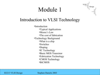
                        Module 1
              Introduction to VLSI Technology
                     •Introduction
                          •Typical Applications
                          •Moore’s Law
                          •The cost of fabrication
                     •Technology Background
                          •What is a chip
                          •Switches
                          •Doping
                          •IC Technology
                          •Basic MOS Transistor
                          •Fabrication Technology
                          •CMOS Technology
                          •BiCMOS


EE213 VLSI Design       Stephen Daniels 2003
VLSI
                                                                              Design


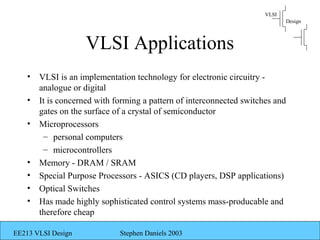
                     VLSI Applications
    •   VLSI is an implementation technology for electronic circuitry -
        analogue or digital
    •   It is concerned with forming a pattern of interconnected switches and
        gates on the surface of a crystal of semiconductor
    •   Microprocessors
         – personal computers
         – microcontrollers
    •   Memory - DRAM / SRAM
    •   Special Purpose Processors - ASICS (CD players, DSP applications)
    •   Optical Switches
    •   Has made highly sophisticated control systems mass-producable and
        therefore cheap

EE213 VLSI Design             Stephen Daniels 2003
VLSI
                                                       Design


                    Moore’s Law
    • Gordon Moore: co-founder of Intel
    • Predicted that the number of transistors per
      chip would grow exponentially (double
      every 18 months)
    • Exponential improvement in technology is a
      natural trend:
        – e.g. Steam Engines - Dynamo - Automobile


EE213 VLSI Design     Stephen Daniels 2003
VLSI
                                                           Design


               The Cost of Fabrication
    • Current cost $2 - 3 billion
    • Typical fab line occupies 1 city block, employees
      a few hundred employees
    • Most profitable period is first 18 months to 2 years
    • For large volume IC’s packaging and testing is
      largest cost
    • For low volume IC’s, design costs may swamp
      manufacturing costs


EE213 VLSI Design     Stephen Daniels 2003
VLSI
                                                  Design


              Technology Background


EE213 VLSI Design   Stephen Daniels 2003
VLSI
                                                                                        Design


                 What is a Silicon Chip?
    •   A pattern of interconnected switches and gates on the surface of a
        crystal of semiconductor (typically Si)
    •   These switches and gates are made of
         –   areas of n-type silicon
         –   areas of p-type silicon
         –   areas of insulator
         –   lines of conductor (interconnects) joining areas together
              • Aluminium, Copper, Titanium, Molybdenum, polysilicon, tungsten
    •    The geometryof these areas is known as the layout of the chip
    •   Connections from the chip to the outside world are made around the
        edge of the chip to facilitate connections to other devices


EE213 VLSI Design                 Stephen Daniels 2003
VLSI
                                                                              Design


                               Switches
    •   Digital equipment is largely composed of switches
    •   Switches can be built from many technologies
         – relays (from which the earliest computers were built)
         – thermionic valves
         – transistors
    • The perfect digital switch would have the following:
         – switch instantly
         – use no power
         – have an infinite resistance when off and zero resistance when on
    • Real switches are not like this!


EE213 VLSI Design             Stephen Daniels 2003
VLSI
                                                                              Design

          Semiconductors and Doping
    • Adding trace amounts of certain materials to
      semiconductors alters the crystal structure and can change
      their electrical properties
        – in particular it can change the number of free electrons or holes
    • N-Type
        – semiconductor has free electrons
        – dopant is (typically) phosphorus, arsenic, antimony
    • P-Type
        – semiconductor has free holes
        – dopant is (typically) boron, indium, gallium
    • Dopants are usually implanted into the semiconductor
      using Implant Technology, followed by thermal process to
      diffuse the dopants
EE213 VLSI Design            Stephen Daniels 2003
VLSI
                                                    Design


                    IC Technology
    • Speed / Power performance of available
      technologies
    • The microelectronics evolution
    • SIA Roadmap
    • Semiconductor Manufacturers 2001
      Ranking


EE213 VLSI Design     Stephen Daniels 2003
Metal-oxide-semiconductor        VLSI
                                                  Design


           (MOS) and related VLSI
                 technology
    •   pMOS
    •   nMOS
    •   CMOS
    •   BiCMOS
    •   GaAs


EE213 VLSI Design   Stephen Daniels 2003
VLSI
                                                   Design


                Basic MOS Transistors
    •   Minimum line width
    •   Transistor cross section
    •   Charge inversion channel
    •   Source connected to substrate
    •   Enhancement vs Depletion mode devices
    •   pMOS are 2.5 time slower than nMOS due
        to electron and hole mobilities

EE213 VLSI Design    Stephen Daniels 2003
VLSI
                                                                         Design


                 Fabrication Technology
    •   Silicon of extremely high purity
         – chemically purified then grown into large crystals
    •   Wafers
         –   crystals are sliced into wafers
         –   wafer diameter is currently 150mm, 200mm, 300mm
         –   wafer thickness <1mm
         –   surface is polished to optical smoothness
    •   Wafer is then ready for processing
    •   Each wafer will yield many chips
         – chip die size varies from about 5mmx5mm to 15mmx15mm
         – A whole wafer is processed at a time


EE213 VLSI Design               Stephen Daniels 2003
VLSI
                                                   Design


               Fabrication Technology
    • Different parts of each die will be made P-
      type or N-type (small amount of other
      atoms intentionally introduced - doping
      -implant)
    • Interconnections are made with metal
    • Insulation used is typically SiO2. SiN is
      also used. New materials being investigated
      (low-k dielectrics)
EE213 VLSI Design    Stephen Daniels 2003
VLSI
                                                    Design


               Fabrication Technology
    • nMOS Fabrication
    • CMOS Fabrication
        – p-well process
        – n-well process
        – twin-tub process


EE213 VLSI Design     Stephen Daniels 2003
VLSI
                                                                                         Design


                Fabrication Technology
    •   All the devices on the wafer are made at the same time
    •   After the circuitry has been placed on the chip
         – the chip is overglassed (with a passivation layer) to protect it
         – only those areas which connect to the outside world will be left uncovered
           (the pads)
    •   The wafer finally passes to a test station
         – test probes send test signal patterns to the chip and monitor the output of
           the chip
    •   The yield of a process is the percentage of die which pass this testing
    •   The wafer is then scribed and separated up into the individual chips.
        These are then packaged
    •   Chips are ‘binned’ according to their performance

EE213 VLSI Design                Stephen Daniels 2003
VLSI
                                                                                  Design


                     CMOS Technology
    •   First proposed in the 1960s. Was not seriously considered until the
        severe limitations in power density and dissipation occurred in NMOS
        circuits
    •   Now the dominant technology in IC manufacturing
    •   Employs both pMOS and nMOS transistors to form logic elements
    •   The advantage of CMOS is that its logic elements draw significant
        current only during the transition from one state to another and very
        little current between transitions - hence power is conserved.
    •   In the case of an inverter, in either logic state one of the transistors is
        off. Since the transistors are in series, (~ no) current flows.
    •   See twin-well cross sections


EE213 VLSI Design               Stephen Daniels 2003
VLSI

                                 BiCMOS                                          Design


    •   A known deficiency of MOS technology is its limited load driving
        capabilities (due to limited current sourcing and sinking abilities of
        pMOS and nMOS transistors.
    •   Bipolar transistors have
         – higher gain
         – better noise characteristics
         – better high frequency characteristics
    •   BiCMOS gates can be an efficient way of speeding up VLSI circuits
    •   See table for comparison between CMOS and BiCMOS
    •   CMOS fabrication process can be extended for BiCMOS
    •   Example Applications
         – CMOS   - Logic
         – BiCMOS - I/O and driver circuits
         – ECL    - critical high speed parts of the system


EE213 VLSI Design               Stephen Daniels 2003

More Related Content

What's hot

Cmos fabrication
Cmos fabricationCmos fabrication
Cmos fabricationKANAGARAJ T
 
CMOS VLSI design
CMOS VLSI designCMOS VLSI design
CMOS VLSI designRajan Kumar
 
Application of VLSI In Artificial Intelligence
Application of VLSI In Artificial IntelligenceApplication of VLSI In Artificial Intelligence
Application of VLSI In Artificial IntelligenceIOSR Journals
 
Introduction to VLSI
Introduction to VLSIIntroduction to VLSI
Introduction to VLSIShams Tabrej
 
Introduction to VLSI
Introduction to VLSI Introduction to VLSI
Introduction to VLSI illpa
 
crosstalk minimisation using vlsi
crosstalk minimisation using vlsicrosstalk minimisation using vlsi
crosstalk minimisation using vlsisubhradeep mitra
 
Analog Layout and Process Concern
Analog Layout and Process ConcernAnalog Layout and Process Concern
Analog Layout and Process Concernasinghsaroj
 
Silicon on Insulator (SOI) Technology
Silicon on Insulator (SOI) TechnologySilicon on Insulator (SOI) Technology
Silicon on Insulator (SOI) TechnologySudhanshu Janwadkar
 
VLSI circuit design process
VLSI circuit design processVLSI circuit design process
VLSI circuit design processVishal kakade
 
chapter-12memory.pptx
chapter-12memory.pptxchapter-12memory.pptx
chapter-12memory.pptxRandomGuy90
 
Vlsi design and fabrication ppt
Vlsi design and fabrication  pptVlsi design and fabrication  ppt
Vlsi design and fabrication pptManjushree Mashal
 
Gate Diffusion Input Technology (Very Large Scale Integration)
Gate Diffusion Input Technology (Very Large Scale Integration)Gate Diffusion Input Technology (Very Large Scale Integration)
Gate Diffusion Input Technology (Very Large Scale Integration)Ashwin Shroff
 
Modified Gate Diffusion Input-MGDI
Modified Gate Diffusion Input-MGDIModified Gate Diffusion Input-MGDI
Modified Gate Diffusion Input-MGDIshubham jha
 
VLSI
VLSI VLSI
VLSI So Ma
 

What's hot (20)

Cmos fabrication
Cmos fabricationCmos fabrication
Cmos fabrication
 
CMOS VLSI design
CMOS VLSI designCMOS VLSI design
CMOS VLSI design
 
Application of VLSI In Artificial Intelligence
Application of VLSI In Artificial IntelligenceApplication of VLSI In Artificial Intelligence
Application of VLSI In Artificial Intelligence
 
Introduction to VLSI
Introduction to VLSIIntroduction to VLSI
Introduction to VLSI
 
Introduction to VLSI
Introduction to VLSI Introduction to VLSI
Introduction to VLSI
 
Finfet Technology
Finfet TechnologyFinfet Technology
Finfet Technology
 
crosstalk minimisation using vlsi
crosstalk minimisation using vlsicrosstalk minimisation using vlsi
crosstalk minimisation using vlsi
 
Analog Layout and Process Concern
Analog Layout and Process ConcernAnalog Layout and Process Concern
Analog Layout and Process Concern
 
Silicon on Insulator (SOI) Technology
Silicon on Insulator (SOI) TechnologySilicon on Insulator (SOI) Technology
Silicon on Insulator (SOI) Technology
 
BGR
BGRBGR
BGR
 
VLSI circuit design process
VLSI circuit design processVLSI circuit design process
VLSI circuit design process
 
Layout02 (1)
Layout02 (1)Layout02 (1)
Layout02 (1)
 
chapter-12memory.pptx
chapter-12memory.pptxchapter-12memory.pptx
chapter-12memory.pptx
 
basic vlsi ppt
basic vlsi pptbasic vlsi ppt
basic vlsi ppt
 
Vlsi design and fabrication ppt
Vlsi design and fabrication  pptVlsi design and fabrication  ppt
Vlsi design and fabrication ppt
 
Gate Diffusion Input Technology (Very Large Scale Integration)
Gate Diffusion Input Technology (Very Large Scale Integration)Gate Diffusion Input Technology (Very Large Scale Integration)
Gate Diffusion Input Technology (Very Large Scale Integration)
 
SILICON ON INSULATOR
SILICON ON INSULATORSILICON ON INSULATOR
SILICON ON INSULATOR
 
Cmos process flow
Cmos process flowCmos process flow
Cmos process flow
 
Modified Gate Diffusion Input-MGDI
Modified Gate Diffusion Input-MGDIModified Gate Diffusion Input-MGDI
Modified Gate Diffusion Input-MGDI
 
VLSI
VLSI VLSI
VLSI
 

Similar to Ee213 vlsi introduction

1. Introduction to PnR.pptx
1. Introduction to PnR.pptx1. Introduction to PnR.pptx
1. Introduction to PnR.pptxAhmed Abdelazeem
 
Arnold Nipper - Building resilient and scalable Terabit Exchangepoints
Arnold Nipper - Building resilient and scalable Terabit ExchangepointsArnold Nipper - Building resilient and scalable Terabit Exchangepoints
Arnold Nipper - Building resilient and scalable Terabit ExchangepointsPROIDEA
 
Vlsi techniques
Vlsi techniquesVlsi techniques
Vlsi techniquesarpit1010
 
SISTec Microelectronics VLSI design
SISTec Microelectronics VLSI designSISTec Microelectronics VLSI design
SISTec Microelectronics VLSI designDr. Ravi Mishra
 
High speed-pcb-board-design-and-analysiscadence-130218085524-phpapp01
High speed-pcb-board-design-and-analysiscadence-130218085524-phpapp01High speed-pcb-board-design-and-analysiscadence-130218085524-phpapp01
High speed-pcb-board-design-and-analysiscadence-130218085524-phpapp01khalid noman husainy
 
Lecture20 asic back_end_design
Lecture20 asic back_end_designLecture20 asic back_end_design
Lecture20 asic back_end_designHung Nguyen
 
Lect2 up010 (100324)
Lect2 up010 (100324)Lect2 up010 (100324)
Lect2 up010 (100324)aicdesign
 
VLSI unit 1 Technology - S.ppt
VLSI unit 1 Technology - S.pptVLSI unit 1 Technology - S.ppt
VLSI unit 1 Technology - S.pptindrajeetPatel22
 
Opticalcomputing final
Opticalcomputing finalOpticalcomputing final
Opticalcomputing finaldivyajyothi405
 

Similar to Ee213 vlsi introduction (20)

1. Introduction to PnR.pptx
1. Introduction to PnR.pptx1. Introduction to PnR.pptx
1. Introduction to PnR.pptx
 
Arnold Nipper - Building resilient and scalable Terabit Exchangepoints
Arnold Nipper - Building resilient and scalable Terabit ExchangepointsArnold Nipper - Building resilient and scalable Terabit Exchangepoints
Arnold Nipper - Building resilient and scalable Terabit Exchangepoints
 
Vlsi techniques
Vlsi techniquesVlsi techniques
Vlsi techniques
 
SISTec Microelectronics VLSI design
SISTec Microelectronics VLSI designSISTec Microelectronics VLSI design
SISTec Microelectronics VLSI design
 
THE CMOS VLSI DESIGN
THE CMOS VLSI DESIGNTHE CMOS VLSI DESIGN
THE CMOS VLSI DESIGN
 
High speed-pcb-board-design-and-analysiscadence-130218085524-phpapp01
High speed-pcb-board-design-and-analysiscadence-130218085524-phpapp01High speed-pcb-board-design-and-analysiscadence-130218085524-phpapp01
High speed-pcb-board-design-and-analysiscadence-130218085524-phpapp01
 
Vlsi td introduction
Vlsi td introductionVlsi td introduction
Vlsi td introduction
 
Lecture01
Lecture01Lecture01
Lecture01
 
intro (1).ppt
intro (1).pptintro (1).ppt
intro (1).ppt
 
Lecture20 asic back_end_design
Lecture20 asic back_end_designLecture20 asic back_end_design
Lecture20 asic back_end_design
 
VLSI Trends.pptx
VLSI Trends.pptxVLSI Trends.pptx
VLSI Trends.pptx
 
1 1 vlsi introduction_overview
1 1 vlsi introduction_overview1 1 vlsi introduction_overview
1 1 vlsi introduction_overview
 
Introduction to ic
Introduction to icIntroduction to ic
Introduction to ic
 
Semiconductor Industry Tutorial
Semiconductor Industry TutorialSemiconductor Industry Tutorial
Semiconductor Industry Tutorial
 
Lect2 up010 (100324)
Lect2 up010 (100324)Lect2 up010 (100324)
Lect2 up010 (100324)
 
VLSI unit 1 Technology - S.ppt
VLSI unit 1 Technology - S.pptVLSI unit 1 Technology - S.ppt
VLSI unit 1 Technology - S.ppt
 
Vlsi design
Vlsi designVlsi design
Vlsi design
 
Opticalcomputing final
Opticalcomputing finalOpticalcomputing final
Opticalcomputing final
 
Lecture44
Lecture44Lecture44
Lecture44
 
vlsi
vlsivlsi
vlsi
 

Recently uploaded

To Graph or Not to Graph Knowledge Graph Architectures and LLMs
To Graph or Not to Graph Knowledge Graph Architectures and LLMsTo Graph or Not to Graph Knowledge Graph Architectures and LLMs
To Graph or Not to Graph Knowledge Graph Architectures and LLMsPaul Groth
 
IOS-PENTESTING-BEGINNERS-PRACTICAL-GUIDE-.pptx
IOS-PENTESTING-BEGINNERS-PRACTICAL-GUIDE-.pptxIOS-PENTESTING-BEGINNERS-PRACTICAL-GUIDE-.pptx
IOS-PENTESTING-BEGINNERS-PRACTICAL-GUIDE-.pptxAbida Shariff
 
Free and Effective: Making Flows Publicly Accessible, Yumi Ibrahimzade
Free and Effective: Making Flows Publicly Accessible, Yumi IbrahimzadeFree and Effective: Making Flows Publicly Accessible, Yumi Ibrahimzade
Free and Effective: Making Flows Publicly Accessible, Yumi IbrahimzadeCzechDreamin
 
Unpacking Value Delivery - Agile Oxford Meetup - May 2024.pptx
Unpacking Value Delivery - Agile Oxford Meetup - May 2024.pptxUnpacking Value Delivery - Agile Oxford Meetup - May 2024.pptx
Unpacking Value Delivery - Agile Oxford Meetup - May 2024.pptxDavid Michel
 
Key Trends Shaping the Future of Infrastructure.pdf
Key Trends Shaping the Future of Infrastructure.pdfKey Trends Shaping the Future of Infrastructure.pdf
Key Trends Shaping the Future of Infrastructure.pdfCheryl Hung
 
From Daily Decisions to Bottom Line: Connecting Product Work to Revenue by VP...
From Daily Decisions to Bottom Line: Connecting Product Work to Revenue by VP...From Daily Decisions to Bottom Line: Connecting Product Work to Revenue by VP...
From Daily Decisions to Bottom Line: Connecting Product Work to Revenue by VP...Product School
 
Kubernetes & AI - Beauty and the Beast !?! @KCD Istanbul 2024
Kubernetes & AI - Beauty and the Beast !?! @KCD Istanbul 2024Kubernetes & AI - Beauty and the Beast !?! @KCD Istanbul 2024
Kubernetes & AI - Beauty and the Beast !?! @KCD Istanbul 2024Tobias Schneck
 
UiPath Test Automation using UiPath Test Suite series, part 2
UiPath Test Automation using UiPath Test Suite series, part 2UiPath Test Automation using UiPath Test Suite series, part 2
UiPath Test Automation using UiPath Test Suite series, part 2DianaGray10
 
Demystifying gRPC in .Net by John Staveley
Demystifying gRPC in .Net by John StaveleyDemystifying gRPC in .Net by John Staveley
Demystifying gRPC in .Net by John StaveleyJohn Staveley
 
Knowledge engineering: from people to machines and back
Knowledge engineering: from people to machines and backKnowledge engineering: from people to machines and back
Knowledge engineering: from people to machines and backElena Simperl
 
Unsubscribed: Combat Subscription Fatigue With a Membership Mentality by Head...
Unsubscribed: Combat Subscription Fatigue With a Membership Mentality by Head...Unsubscribed: Combat Subscription Fatigue With a Membership Mentality by Head...
Unsubscribed: Combat Subscription Fatigue With a Membership Mentality by Head...Product School
 
Optimizing NoSQL Performance Through Observability
Optimizing NoSQL Performance Through ObservabilityOptimizing NoSQL Performance Through Observability
Optimizing NoSQL Performance Through ObservabilityScyllaDB
 
UiPath Test Automation using UiPath Test Suite series, part 1
UiPath Test Automation using UiPath Test Suite series, part 1UiPath Test Automation using UiPath Test Suite series, part 1
UiPath Test Automation using UiPath Test Suite series, part 1DianaGray10
 
Integrating Telephony Systems with Salesforce: Insights and Considerations, B...
Integrating Telephony Systems with Salesforce: Insights and Considerations, B...Integrating Telephony Systems with Salesforce: Insights and Considerations, B...
Integrating Telephony Systems with Salesforce: Insights and Considerations, B...CzechDreamin
 
Introduction to Open Source RAG and RAG Evaluation
Introduction to Open Source RAG and RAG EvaluationIntroduction to Open Source RAG and RAG Evaluation
Introduction to Open Source RAG and RAG EvaluationZilliz
 
Custom Approval Process: A New Perspective, Pavel Hrbacek & Anindya Halder
Custom Approval Process: A New Perspective, Pavel Hrbacek & Anindya HalderCustom Approval Process: A New Perspective, Pavel Hrbacek & Anindya Halder
Custom Approval Process: A New Perspective, Pavel Hrbacek & Anindya HalderCzechDreamin
 
Empowering NextGen Mobility via Large Action Model Infrastructure (LAMI): pav...
Empowering NextGen Mobility via Large Action Model Infrastructure (LAMI): pav...Empowering NextGen Mobility via Large Action Model Infrastructure (LAMI): pav...
Empowering NextGen Mobility via Large Action Model Infrastructure (LAMI): pav...Thierry Lestable
 
From Siloed Products to Connected Ecosystem: Building a Sustainable and Scala...
From Siloed Products to Connected Ecosystem: Building a Sustainable and Scala...From Siloed Products to Connected Ecosystem: Building a Sustainable and Scala...
From Siloed Products to Connected Ecosystem: Building a Sustainable and Scala...Product School
 
UiPath Test Automation using UiPath Test Suite series, part 3
UiPath Test Automation using UiPath Test Suite series, part 3UiPath Test Automation using UiPath Test Suite series, part 3
UiPath Test Automation using UiPath Test Suite series, part 3DianaGray10
 
SOQL 201 for Admins & Developers: Slice & Dice Your Org’s Data With Aggregate...
SOQL 201 for Admins & Developers: Slice & Dice Your Org’s Data With Aggregate...SOQL 201 for Admins & Developers: Slice & Dice Your Org’s Data With Aggregate...
SOQL 201 for Admins & Developers: Slice & Dice Your Org’s Data With Aggregate...CzechDreamin
 

Recently uploaded (20)

To Graph or Not to Graph Knowledge Graph Architectures and LLMs
To Graph or Not to Graph Knowledge Graph Architectures and LLMsTo Graph or Not to Graph Knowledge Graph Architectures and LLMs
To Graph or Not to Graph Knowledge Graph Architectures and LLMs
 
IOS-PENTESTING-BEGINNERS-PRACTICAL-GUIDE-.pptx
IOS-PENTESTING-BEGINNERS-PRACTICAL-GUIDE-.pptxIOS-PENTESTING-BEGINNERS-PRACTICAL-GUIDE-.pptx
IOS-PENTESTING-BEGINNERS-PRACTICAL-GUIDE-.pptx
 
Free and Effective: Making Flows Publicly Accessible, Yumi Ibrahimzade
Free and Effective: Making Flows Publicly Accessible, Yumi IbrahimzadeFree and Effective: Making Flows Publicly Accessible, Yumi Ibrahimzade
Free and Effective: Making Flows Publicly Accessible, Yumi Ibrahimzade
 
Unpacking Value Delivery - Agile Oxford Meetup - May 2024.pptx
Unpacking Value Delivery - Agile Oxford Meetup - May 2024.pptxUnpacking Value Delivery - Agile Oxford Meetup - May 2024.pptx
Unpacking Value Delivery - Agile Oxford Meetup - May 2024.pptx
 
Key Trends Shaping the Future of Infrastructure.pdf
Key Trends Shaping the Future of Infrastructure.pdfKey Trends Shaping the Future of Infrastructure.pdf
Key Trends Shaping the Future of Infrastructure.pdf
 
From Daily Decisions to Bottom Line: Connecting Product Work to Revenue by VP...
From Daily Decisions to Bottom Line: Connecting Product Work to Revenue by VP...From Daily Decisions to Bottom Line: Connecting Product Work to Revenue by VP...
From Daily Decisions to Bottom Line: Connecting Product Work to Revenue by VP...
 
Kubernetes & AI - Beauty and the Beast !?! @KCD Istanbul 2024
Kubernetes & AI - Beauty and the Beast !?! @KCD Istanbul 2024Kubernetes & AI - Beauty and the Beast !?! @KCD Istanbul 2024
Kubernetes & AI - Beauty and the Beast !?! @KCD Istanbul 2024
 
UiPath Test Automation using UiPath Test Suite series, part 2
UiPath Test Automation using UiPath Test Suite series, part 2UiPath Test Automation using UiPath Test Suite series, part 2
UiPath Test Automation using UiPath Test Suite series, part 2
 
Demystifying gRPC in .Net by John Staveley
Demystifying gRPC in .Net by John StaveleyDemystifying gRPC in .Net by John Staveley
Demystifying gRPC in .Net by John Staveley
 
Knowledge engineering: from people to machines and back
Knowledge engineering: from people to machines and backKnowledge engineering: from people to machines and back
Knowledge engineering: from people to machines and back
 
Unsubscribed: Combat Subscription Fatigue With a Membership Mentality by Head...
Unsubscribed: Combat Subscription Fatigue With a Membership Mentality by Head...Unsubscribed: Combat Subscription Fatigue With a Membership Mentality by Head...
Unsubscribed: Combat Subscription Fatigue With a Membership Mentality by Head...
 
Optimizing NoSQL Performance Through Observability
Optimizing NoSQL Performance Through ObservabilityOptimizing NoSQL Performance Through Observability
Optimizing NoSQL Performance Through Observability
 
UiPath Test Automation using UiPath Test Suite series, part 1
UiPath Test Automation using UiPath Test Suite series, part 1UiPath Test Automation using UiPath Test Suite series, part 1
UiPath Test Automation using UiPath Test Suite series, part 1
 
Integrating Telephony Systems with Salesforce: Insights and Considerations, B...
Integrating Telephony Systems with Salesforce: Insights and Considerations, B...Integrating Telephony Systems with Salesforce: Insights and Considerations, B...
Integrating Telephony Systems with Salesforce: Insights and Considerations, B...
 
Introduction to Open Source RAG and RAG Evaluation
Introduction to Open Source RAG and RAG EvaluationIntroduction to Open Source RAG and RAG Evaluation
Introduction to Open Source RAG and RAG Evaluation
 
Custom Approval Process: A New Perspective, Pavel Hrbacek & Anindya Halder
Custom Approval Process: A New Perspective, Pavel Hrbacek & Anindya HalderCustom Approval Process: A New Perspective, Pavel Hrbacek & Anindya Halder
Custom Approval Process: A New Perspective, Pavel Hrbacek & Anindya Halder
 
Empowering NextGen Mobility via Large Action Model Infrastructure (LAMI): pav...
Empowering NextGen Mobility via Large Action Model Infrastructure (LAMI): pav...Empowering NextGen Mobility via Large Action Model Infrastructure (LAMI): pav...
Empowering NextGen Mobility via Large Action Model Infrastructure (LAMI): pav...
 
From Siloed Products to Connected Ecosystem: Building a Sustainable and Scala...
From Siloed Products to Connected Ecosystem: Building a Sustainable and Scala...From Siloed Products to Connected Ecosystem: Building a Sustainable and Scala...
From Siloed Products to Connected Ecosystem: Building a Sustainable and Scala...
 
UiPath Test Automation using UiPath Test Suite series, part 3
UiPath Test Automation using UiPath Test Suite series, part 3UiPath Test Automation using UiPath Test Suite series, part 3
UiPath Test Automation using UiPath Test Suite series, part 3
 
SOQL 201 for Admins & Developers: Slice & Dice Your Org’s Data With Aggregate...
SOQL 201 for Admins & Developers: Slice & Dice Your Org’s Data With Aggregate...SOQL 201 for Admins & Developers: Slice & Dice Your Org’s Data With Aggregate...
SOQL 201 for Admins & Developers: Slice & Dice Your Org’s Data With Aggregate...
 

Ee213 vlsi introduction

  • 1. VLSI Design Module Aims • Introduction to VLSI Technology – Process Design • Trends • Chip Fabrication • Real Circuit Parameters – Circuit Design • Electrical Characteristics • Configuration Building Blocks • Switching Circuitry • Translation onto Silicon • CAD – Practical Experience in Layout Design EE213 VLSI Design Stephen Daniels 2003
  • 2. VLSI Design Learning Outcomes • Understand the principles of the design and implementation of standard MOS integrated circuits and be able to assess their performance taking into account the effects of real circuit parameters EE213 VLSI Design Stephen Daniels 2003
  • 3. VLSI Design Laboratory • Microwind layout and simulation package • Dedicated to training in sub-micron CMOS VLSI design • Layout editor, electrical circuit extractor and on-line analogue simulator EE213 VLSI Design Stephen Daniels 2003
  • 4. VLSI Design Reading List • Introduction to Microelectronics – http://intrage.insa-tlse.fr~etienne/Microwind • Introduction to VLSI Design – ED Fabricius – McGraw-Hill, 1990 ISBN 0-07-19948-5 • Basic VLSI Design – D. A. Pucknell, K Eshraghian – Prentice Hall, 1994 ISBN 0-13-079153-9 EE213 VLSI Design Stephen Daniels 2003
  • 5. VLSI Design Why VLSI? • Integration improves the design – Lower parasitics = higher speed – Lower power consumption – Physically smaller • Integration reduces manufacturing cost - (almost) no manual assembly EE213 VLSI Design Stephen Daniels 2003
  • 6. VLSI Design Module 1 Introduction to VLSI Technology •Introduction •Typical Applications •Moore’s Law •The cost of fabrication •Technology Background •What is a chip •Switches •Doping •IC Technology •Basic MOS Transistor •Fabrication Technology •CMOS Technology •BiCMOS EE213 VLSI Design Stephen Daniels 2003
  • 7. VLSI Design VLSI Applications • VLSI is an implementation technology for electronic circuitry - analogue or digital • It is concerned with forming a pattern of interconnected switches and gates on the surface of a crystal of semiconductor • Microprocessors – personal computers – microcontrollers • Memory - DRAM / SRAM • Special Purpose Processors - ASICS (CD players, DSP applications) • Optical Switches • Has made highly sophisticated control systems mass-producable and therefore cheap EE213 VLSI Design Stephen Daniels 2003
  • 8. VLSI Design Moore’s Law • Gordon Moore: co-founder of Intel • Predicted that the number of transistors per chip would grow exponentially (double every 18 months) • Exponential improvement in technology is a natural trend: – e.g. Steam Engines - Dynamo - Automobile EE213 VLSI Design Stephen Daniels 2003
  • 9. VLSI Design The Cost of Fabrication • Current cost $2 - 3 billion • Typical fab line occupies 1 city block, employees a few hundred employees • Most profitable period is first 18 months to 2 years • For large volume IC’s packaging and testing is largest cost • For low volume IC’s, design costs may swamp manufacturing costs EE213 VLSI Design Stephen Daniels 2003
  • 10. VLSI Design Technology Background EE213 VLSI Design Stephen Daniels 2003
  • 11. VLSI Design What is a Silicon Chip? • A pattern of interconnected switches and gates on the surface of a crystal of semiconductor (typically Si) • These switches and gates are made of – areas of n-type silicon – areas of p-type silicon – areas of insulator – lines of conductor (interconnects) joining areas together • Aluminium, Copper, Titanium, Molybdenum, polysilicon, tungsten • The geometryof these areas is known as the layout of the chip • Connections from the chip to the outside world are made around the edge of the chip to facilitate connections to other devices EE213 VLSI Design Stephen Daniels 2003
  • 12. VLSI Design Switches • Digital equipment is largely composed of switches • Switches can be built from many technologies – relays (from which the earliest computers were built) – thermionic valves – transistors • The perfect digital switch would have the following: – switch instantly – use no power – have an infinite resistance when off and zero resistance when on • Real switches are not like this! EE213 VLSI Design Stephen Daniels 2003
  • 13. VLSI Design Semiconductors and Doping • Adding trace amounts of certain materials to semiconductors alters the crystal structure and can change their electrical properties – in particular it can change the number of free electrons or holes • N-Type – semiconductor has free electrons – dopant is (typically) phosphorus, arsenic, antimony • P-Type – semiconductor has free holes – dopant is (typically) boron, indium, gallium • Dopants are usually implanted into the semiconductor using Implant Technology, followed by thermal process to diffuse the dopants EE213 VLSI Design Stephen Daniels 2003
  • 14. VLSI Design IC Technology • Speed / Power performance of available technologies • The microelectronics evolution • SIA Roadmap • Semiconductor Manufacturers 2001 Ranking EE213 VLSI Design Stephen Daniels 2003
  • 15. Metal-oxide-semiconductor VLSI Design (MOS) and related VLSI technology • pMOS • nMOS • CMOS • BiCMOS • GaAs EE213 VLSI Design Stephen Daniels 2003
  • 16. VLSI Design Basic MOS Transistors • Minimum line width • Transistor cross section • Charge inversion channel • Source connected to substrate • Enhancement vs Depletion mode devices • pMOS are 2.5 time slower than nMOS due to electron and hole mobilities EE213 VLSI Design Stephen Daniels 2003
  • 17. VLSI Design Fabrication Technology • Silicon of extremely high purity – chemically purified then grown into large crystals • Wafers – crystals are sliced into wafers – wafer diameter is currently 150mm, 200mm, 300mm – wafer thickness <1mm – surface is polished to optical smoothness • Wafer is then ready for processing • Each wafer will yield many chips – chip die size varies from about 5mmx5mm to 15mmx15mm – A whole wafer is processed at a time EE213 VLSI Design Stephen Daniels 2003
  • 18. VLSI Design Fabrication Technology • Different parts of each die will be made P- type or N-type (small amount of other atoms intentionally introduced - doping -implant) • Interconnections are made with metal • Insulation used is typically SiO2. SiN is also used. New materials being investigated (low-k dielectrics) EE213 VLSI Design Stephen Daniels 2003
  • 19. VLSI Design Fabrication Technology • nMOS Fabrication • CMOS Fabrication – p-well process – n-well process – twin-tub process EE213 VLSI Design Stephen Daniels 2003
  • 20. VLSI Design Fabrication Technology • All the devices on the wafer are made at the same time • After the circuitry has been placed on the chip – the chip is overglassed (with a passivation layer) to protect it – only those areas which connect to the outside world will be left uncovered (the pads) • The wafer finally passes to a test station – test probes send test signal patterns to the chip and monitor the output of the chip • The yield of a process is the percentage of die which pass this testing • The wafer is then scribed and separated up into the individual chips. These are then packaged • Chips are ‘binned’ according to their performance EE213 VLSI Design Stephen Daniels 2003
  • 21. VLSI Design CMOS Technology • First proposed in the 1960s. Was not seriously considered until the severe limitations in power density and dissipation occurred in NMOS circuits • Now the dominant technology in IC manufacturing • Employs both pMOS and nMOS transistors to form logic elements • The advantage of CMOS is that its logic elements draw significant current only during the transition from one state to another and very little current between transitions - hence power is conserved. • In the case of an inverter, in either logic state one of the transistors is off. Since the transistors are in series, (~ no) current flows. • See twin-well cross sections EE213 VLSI Design Stephen Daniels 2003
  • 22. VLSI BiCMOS Design • A known deficiency of MOS technology is its limited load driving capabilities (due to limited current sourcing and sinking abilities of pMOS and nMOS transistors. • Bipolar transistors have – higher gain – better noise characteristics – better high frequency characteristics • BiCMOS gates can be an efficient way of speeding up VLSI circuits • See table for comparison between CMOS and BiCMOS • CMOS fabrication process can be extended for BiCMOS • Example Applications – CMOS - Logic – BiCMOS - I/O and driver circuits – ECL - critical high speed parts of the system EE213 VLSI Design Stephen Daniels 2003