The document describes technical specifications for multi-function watt-hour meter communication, including physical layer specifications for different interface types (infrared light, serial port), frame formats, and data identifier codes. It defines specifications for signal levels, transfer speeds, frame structure with start/end flags, address fields, error checking, and a four-level tree data structure using a two-byte identifier code to represent different data types and attributes.
Flipflops and Excitation tables of flipflopsstudent
This document discusses latches and flip-flops. It explains that gates perform logic operations while flip-flops can store binary values. There are two types of sequential logic circuits: combinational using gates and sequential using flip-flops like the SR, D, JK, and T flip-flops. Flip-flops change state based on clock pulses in synchronous circuits or independent of clocks in asynchronous circuits.
This document defines and describes network functions for one-port and two-port networks. It explains that a one-port network has a single terminal pair that can be represented by a driving point impedance or admittance function. A two-port network has input and output ports, and can be characterized by various matrix parameters including impedance, admittance, transmission, and hybrid parameters. The document also defines driving point and transfer functions that describe the relationships between voltages and currents at the ports of a two-port network.
The document discusses VLSI (Very Large Scale Integration) systems and the VLSI design flow. VLSI systems integrate millions of electronic components into a small chip area. The objectives of VLSI design are high circuit speed, low power consumption, and minimizing design area. The VLSI design flow involves idea conception, specifying requirements, designing architecture, register transfer level coding in VHDL, RTL verification through simulation, synthesis into logic gates, sending to a foundry for fabrication, and producing the final integrated circuit chip.
The document discusses information theory and source coding. It defines information and entropy, explaining that the amount of information contained in a message depends on its probability. The entropy of a data source measures the average information content. Huffman coding is presented as a method to assign variable-length codes to symbols to minimize the average code length. Error detection and correction codes are also summarized, including parity checking, cyclic redundancy checks (CRC), linear block codes, and convolutional codes.
1. Flip-flops and latches are types of memory elements used in sequential circuits. Latches change state based on input levels while flip-flops change state only on the rising or falling edge of a clock signal.
2. Common types of latches include the SR latch and D latch. Common types of flip-flops include the D flip-flop, JK flip-flop, and T flip-flop. Each has a characteristic truth table that defines its operation.
3. Sequential circuits can be analyzed using state tables that define the next state based on the present state and inputs. The state is defined by the values stored in all memory elements of the circuit.
Interfacing methods of microcontrollerDiwaker Pant
The document discusses microcontroller interfacing. It defines interfacing as the transfer of data between microcontrollers and peripherals using buses. Interfacing is needed to connect a microcontroller's computation capabilities to external signals or devices to enable man-machine interaction. Various interfacing methods are described, including wiring techniques like wires, buses, and pins. Examples of interfacing a microcontroller to memory and I/O devices are provided. Common microcontroller interfaces like digital input/output, analog, serial interfaces are also summarized along with their applications and advantages/disadvantages.
The document describes a two port network and provides information about various parameter representations of two port networks, including:
- Z parameters define the input and transfer impedances between the two ports.
- Y parameters define the input and transfer admittances between the two ports.
- Transmission parameters (A,B,C,D) define relationships between voltages and currents at the two ports.
- Hybrid parameters also define relationships between voltages and currents at the two ports.
Examples are provided to demonstrate calculating the parameter representations for given two port networks. Additionally, the document discusses how modifying a two port network impacts its parameter representations.
This document describes a student project to implement frequency shift keying (FSK) modulation using two 555 timer circuits. The first 555 timer generates a digital signal at a defined frequency. The second 555 timer circuit modulates this signal to shift between two mark-space frequencies, controlled by a BC-547 transistor switching between logic 1 and 0 levels. The project analyzes the circuit operation and resulting modulated signal. Applications of FSK modulation discussed include early modems, radio transmission, and local area networks.
Introduction to Digital Signal processorsPeriyanayagiS
- Digital signal processors are specialized microprocessors targeted at digital signal processing applications that require real-time processing. They have hardware features like multipliers, modified bus structures, and pipelining that enable efficient DSP operations.
- Common DSP processors include fixed-point and floating-point processors from Texas Instruments and Analog Devices. DSP architectures include Harvard, modified Harvard, and VLIW to enable parallel instruction execution. Special DSP instructions and addressing modes also aid fast computations.
- The TMS320C5x is a 16-bit fixed-point DSP processor family with a Harvard architecture, single-cycle MAC unit, and on-chip memory that has been used in applications like audio processing, communications,
Logical Instructions used in 8086 microprocessorRabin BK
It contains all the types of instruction required for performing logical operation in 8086 microprocessor. It is useful from the examination point of view as well.
flip flop,introduction,types,. SR Flip Flop
a.SR Flip Flop Active Low = NAND gate Latch
b. SR Flip Flop Active High = NOR gate Latch
2. Clocked SR Flip Flop
3. JK Flip Flop
4. JK Flip Flop With Pre-set And Clear
5. T Flip Flop
6. D Flip Flop
7. Master-Slave Edge-Triggered Flip-Flop
The Used of Flip Flop:
The document discusses the Silicon Controlled Rectifier (SCR), which acts as a switch that is cheaper than a relay and can handle large power dissipation. The SCR has a four-layer construction like a conventional rectifier but includes a third gate terminal that controls the rectifier conduction. When a positive voltage is applied to the anode and gate, current will flow through the device, turning it on. Once on, it remains on even after the gate signal is removed, as long as the minimum holding current is maintained.
This document discusses various parameters used to characterize two-port networks, including Z, Y, S, and ABCD parameters. It explains that Z parameters relate voltages and currents using an impedance matrix, while Y parameters use an admittance matrix. S parameters describe the scattering of waves at the ports in terms of reflection and transmission coefficients. The ABCD matrix relates voltages and currents at the ports and allows for easy cascading of networks. Measurements are typically made using a vector network analyzer to determine the S-parameter scattering matrix.
Tutorial acondicionamiento de señales digitales para microcontroladoresivmarquez
Este documento presenta cuatro ejemplos de circuitos para acondicionar señales digitales para su uso con microcontroladores. Los ejemplos utilizan optoacopladores, relés y transistores Darlington para controlar cargas que requieren voltajes mayores a 5V, como motores, lámparas y bombillas. El estudiante debe simular los circuitos en Proteus para comprender cómo manejan señales de entrada y salida entre dispositivos con diferentes niveles de voltaje.
Hardware description languages (HDLs) allow designers to describe digital systems at different levels of abstraction in a textual format. The two most commonly used HDLs are Verilog and VHDL. Verilog is commonly used in the US, while VHDL is more popular in Europe. HDLs enable simulation of designs before fabrication to verify functionality. Digital designs can be modeled at the gate level, data flow level, or behavioral level in Verilog. Verilog code consists of a design module and test bench module to stimulate inputs and observe outputs.
The document discusses UART (Universal Asynchronous Receiver/Transmitter) communication. It describes how UARTs allow for asynchronous serial communication between devices using only 2 wires by converting parallel data to serial and vice versa. The UART communication process involves a transmitting UART adding start, stop and optionally parity bits to data before transmitting it serially bit-by-bit to a receiving UART which reconstructs the parallel data. It also discusses the TTL and RS-232 physical layer standards for UART.
Flip-flops are basic memory circuits that have two stable states and can store one bit of information. There are several types of flip-flops including SR, JK, D, and T. The SR flip-flop has two inputs called set and reset that determine its output state, while the JK flip-flop's J and K inputs can toggle its output. Flip-flops like the D and JK can be constructed from more basic flip-flops. For sequential circuits, flip-flops are made synchronous using a clock input so their state only changes at the clock edge.
This document discusses latches and flip-flops. It describes the SR latch, gated SR latch, D latch, and gated D latch. It also covers edge-triggered flip-flops including the SR, D, and JK flip-flops. The key uses of flip-flops are for data storage, data transfer, counting, and frequency division in digital circuits and sequential logic.
The document discusses the Quine-McCluskey method for minimizing Boolean functions. It begins with an example that shows the steps of the method applied to a function with 4 variables. The steps include: 1) grouping minterms, 2) merging minterms between groups, 3) repeating merging until no more is possible, 4) creating a prime implicant table, 5) identifying essential minterms and prime implicants, and 6) adding prime implicants to create the minimum expression. The example results in a minimum expression of WXZ + WYZ + XYZ + XZ + WXY.
This document provides an overview of sequential circuits such as latches and flip-flops. It defines sequential circuits and explains that they produce outputs based on current and previous inputs. The basic types of latches and flip-flops are described as SR, D, JK, and T. Characteristics of synchronous and asynchronous sequential circuits are also summarized. Common applications of sequential circuits include shift registers, counters, clocks, and storing temporary information in microprocessors. The document concludes by discussing specific sequential circuit components like SR latches, D flip-flops, and JK flip-flops in more detail.
1) Verilog allows parameters and localparams to define constants in modules. Parameters can alter module behavior when their values change, while localparam values cannot change.
2) System tasks like $display and $monitor are used for outputting values and monitoring signals. $stop and $finish control simulation execution.
3) Compiler directives like `define, `include, `ifdef and `timescale are used to define macros, include files, and make conditional compilations in Verilog.
Base band transmission
*Wave form representation of binary digits
*PCM, DPCM, DM, ADM systems
*Detection of signals in Gaussian noise
*Matched filter - Application of matched filter
*Error probability performance of binary signaling
*Multilevel base band transmission
*Inter symbol interference
*Eye pattern
*Companding
*A law and μ law
*Correlation receiver
The document discusses flip-flops, which are basic electronic circuits that have two stable states and can serve as one bit of digital memory. It defines what a flip-flop is and describes several common types of flip-flops, including SR, JK, T, D, and master-slave edge-triggered flip-flops. The document provides brief explanations of how each flip-flop type works and is implemented using logic gates.
A register is a group of flip-flops that can store multiple bits of data. There are four types of shift registers: serial-in serial-out (SISO), serial-in parallel-out (SIPO), parallel-in serial-out (PISO), and parallel-in parallel-out (PIPO). Shift registers allow data to move between flip-flops on each clock pulse. Ring counters and Johnson counters are examples of shift register counters that produce repeating output sequences.
Logical instruction of 8085
Instruction Set of 8085
Classification of Instruction Set
Logical Instructions
AND, OR, XOR
Logical Instructions
Summary Logical Group
Current sources, current mirrors, and current steering circuits are important components in integrated circuit design for providing stable bias currents. A constant current is first generated and then replicated across the circuit using current mirrors. Current mirrors use identical MOS transistors such that if the gate-source potentials are equal, the drain currents will be equal, allowing the reference current to be copied. There are various types of current mirror circuits that have different advantages and applications. Current can also be steered between paths using multiple current mirrors, with some mirrors acting as current sources and others as current sinks.
This document provides information about the diac, including its structure, operation, and applications. It discusses how a diac is a bidirectional semiconductor device that can be switched from an OFF state to an ON state with either polarity of applied voltage. When the applied voltage exceeds the breakover voltage, the diac begins conducting. Diacs are commonly used to trigger triacs in applications like light dimmers and heat controls to smoothly vary the output voltage through phase control of AC power.
Hands On Data Communications, Networking and TCP/IP TroubleshootingLiving Online
More and more people who work in plants need to understand how data from the field is transmitted to the control room and even to Manufacturing Execution Systems located in head offices situated considerable distances from the plant. It is a technological marvel and this manual helps you to understand the flow of information and the various techniques involved in it.
MORE INFORMATION: http://www.idc-online.com/content/hands-data-communications-networking-and-tcpip-troubleshooting-30?id=37
This document provides information about Eastron's SDM230Modbus smart meter and its implementation of the Modbus protocol for communication. It describes the electrical interface for the RS485 connection and details the input and holding registers used to access meter values and configuration settings using Modbus functions like read input register, read holding register, and write multiple registers. Tables list the Modbus address of each meter parameter that can be accessed.
This document discusses serial communication between an 8051 microcontroller and a PC. It describes the registers involved in serial communication like SCON and TMOD. It explains how to set the baud rate using Timer1. A level converter chip like MAX232 is needed to convert voltage levels between serial ports and microcontrollers. The document provides code examples to transmit and receive data through the serial port. It discusses connecting the microcontroller to a PC using a serial cable and level shifter for debugging serial communication.
The document discusses two common industrial communication protocols: MODBUS and CANBUS. MODBUS uses a master-slave architecture and transmits data via MODBUS RTU, TCP/IP, or ASCII. It stores information in registers and coils that devices can read from and write to. CANBUS was developed for automotive applications to replace point-to-point wiring with a standardized serial bus. It uses dominant and recessive states to transmit data frames with identifiers, data, and CRC across a bus without a master. Both protocols are now widely used for industrial automation and embedded systems.
Cell Phone Controlled Home Automation System using DTMF TechnologyTaufique Sekh
This home appliances control or home automation project uses DTMF decoder circuit to control home and office electrical appliances. Just connect your cell phone headset (headphone) jack to the mobile phone and then mobile will control electrical appliances and electrical equipment through the DTMF key pad of your cell phone. Here for demonstrating, we are controlling an electrical bulb using this circuit project but you can extend this circuit to control many electrical devices with some modifications using4×16 decoder IC.
"Emblogic.com" is the best education center in India to assist you about serial port device driver and their development as well. To know more about these kind of training program, visit our professional website.
This document summarizes circuit switching and packet switching techniques in communications networks. It discusses how circuit switching establishes a dedicated physical path between communicating nodes but is inefficient for bursty traffic. Packet switching breaks messages into packets that are transmitted over shared links, improving efficiency. Key aspects covered include virtual circuits, datagrams, packet switching advantages, X.25 standards, and how Frame Relay improved on X.25 by reducing overhead.
This document describes a project to control industrial/agricultural loads wirelessly using cell phones. The receiving phone decodes DTMF tones from the sending phone using a decoder chip. The output is fed to a microcontroller which controls relays and loads. A power supply regulates voltage for the microcontroller and other ICs. Relay driver chips interface the microcontroller to the relays. The project allows remote control of loads from any location using basic cell phones.
This document provides information about a wireless serial communication RF modem module that operates at 2.4 GHz with a range of 30 meters. It can transmit and receive data at multiple baud rates and supports half-duplex communication. The module has features such as multiple channel selection, operation in the unlicensed 2.4 GHz band, and a standard UART interface. Example applications and specifications are also provided, along with code samples for interfacing the module with an 8051 microcontroller and a PC.
This document provides information about a wireless serial communication RF modem module that operates at 2.4 GHz with a range of 30 meters. It can transmit and receive data at multiple baud rates and supports half-duplex communication. The module has features such as multiple channel selection, compatibility with the unlicensed 2.4 GHz ISM band, and plug-and-play operation. Specifications, pinouts, operating instructions, and code examples for interfacing the module with an 8051 microcontroller and PC are also included.
The document describes the design of a multimeter using VHDL. The multimeter will have four modes - voltmeter, ammeter, ohmmeter, and beta calculator. It will use an Altera DE2 board programmed with VHDL code to control the logic and display measurements on LEDs and an LCD. The VHDL code will control the states and registers to manipulate the different modes. Additional circuits including a power supply, integrating amplifier, and resistance circuits will be used to measure voltage, current, resistance, and beta. Work has begun on the VHDL code and circuit designs, while future work includes completing the circuit designs and testing the integrated system.
This document discusses serial communication and programming the serial port of the 8051 microcontroller. It describes the basics of serial vs parallel communication, synchronous vs asynchronous transmission, and data framing. It also covers connecting the 8051 serial port to RS-232 via a MAX232 chip, programming the baud rate using Timer 1, and using registers like SBUF, SCON, TMOD, and flags to transmit and receive data.
The document discusses various peripherals that can be interfaced with microcontrollers, including the 8255 Programmable Peripheral Interface (PPI), ADC0809 analog to digital converter, DAC0800 digital to analog converter, and serial communication standards like RS-232. It provides details on the architecture and interfacing of the 8255 PPI and describes how its ports are selected and programmed. It also provides interfacing diagrams and example programs for interfacing the 8255 with an 8051 microcontroller, as well as for interfacing the ADC0809 and DAC0800 for analog to digital and digital to analog conversion respectively. Finally, it discusses serial communication standards like RS-232, RS-485, RS-
The document discusses serial port programming for the 8051 microcontroller. It describes how serial communication works using one bit at a time instead of parallel communication which transfers all bits at once. It explains the registers and pins used for serial communication on the 8051 including the SBUF, SCON, TMOD registers and MAX232 voltage converter. It provides details on programming the 8051 for serial data transmission and reception by monitoring the TI and RI flags in the SCON register.
The document discusses serial port programming for the 8051 microcontroller. It describes how serial communication works using one bit at a time instead of parallel communication which transfers all bits at once. It explains the registers and pins used for serial communication on the 8051 including the serial data buffer (SBUF) register, serial control (SCON) register, and MAX232 voltage converter. It provides details on programming the 8051 for serial data transmission and reception, including using the TI and RI flags to indicate when data has been sent or received.
The document discusses interfacing a microcontroller with various peripherals including timers, serial communication, interrupts, LCDs, and keyboards. It provides details on:
- Programming timers in 8051 microcontrollers for time delays and waveform generation.
- Serial communication protocols including asynchronous communication and RS-232 standards.
- Configuring and handling interrupts from different sources and writing interrupt service routines.
- Interfacing 8051 with LCDs for display and matrix keyboards for input using specific I/O ports for scanning rows and columns.
UNIT 4 & 5 - I nterfacing_Lecture7.pptxnaveen088888
The document discusses analog sensor interfacing and analog to digital conversion. It explains that physical quantities in the real world are analog while computers use digital values, so an analog to digital converter (ADC) is used to convert analog sensor signals to digital values. It then describes the characteristics of ADCs like resolution, conversion time, reference voltage, and output data format. It provides examples of calculating the step size and digital output for different resolutions and reference voltages. Finally, it discusses different types of sensors, interfacing techniques for sensors, displays, and relays with microcontrollers.
Data Encoding for Wireless TransmissionSean McQuay
This project aims to develop a low-cost wireless transmitter/receiver pair using an inexpensive AVR microcontroller to implement error correction software. The transmitter will encode data using a forward error correction algorithm before transmission. The receiver will decode the received data and attempt to correct up to three bit errors per byte. Additionally, an addressing scheme will be implemented to allow multiple transmitters to communicate with a single receiver. The total cost of the redesigned transmitter/receiver pair is intended to remain under $10.
This document discusses 8051 serial communication. It describes the key features of 8051 serial communication including full-duplex communication and special function registers. It explains the four different modes of operation and how to double the baud rate. It also provides details on connecting the 8051 to RS232 using a MAX232 chip and provides examples of programs for serial communication.
How information systems are built or acquired puts information, which is what they should be about, in a secondary place. Our language adapted accordingly, and we no longer talk about information systems but applications. Applications evolved in a way to break data into diverse fragments, tightly coupled with applications and expensive to integrate. The result is technical debt, which is re-paid by taking even bigger "loans", resulting in an ever-increasing technical debt. Software engineering and procurement practices work in sync with market forces to maintain this trend. This talk demonstrates how natural this situation is. The question is: can something be done to reverse the trend?
In the realm of cybersecurity, offensive security practices act as a critical shield. By simulating real-world attacks in a controlled environment, these techniques expose vulnerabilities before malicious actors can exploit them. This proactive approach allows manufacturers to identify and fix weaknesses, significantly enhancing system security.
This presentation delves into the development of a system designed to mimic Galileo's Open Service signal using software-defined radio (SDR) technology. We'll begin with a foundational overview of both Global Navigation Satellite Systems (GNSS) and the intricacies of digital signal processing.
The presentation culminates in a live demonstration. We'll showcase the manipulation of Galileo's Open Service pilot signal, simulating an attack on various software and hardware systems. This practical demonstration serves to highlight the potential consequences of unaddressed vulnerabilities, emphasizing the importance of offensive security practices in safeguarding critical infrastructure.
What is an RPA CoE? Session 2 – CoE RolesDianaGray10
In this session, we will review the players involved in the CoE and how each role impacts opportunities.
Topics covered:
• What roles are essential?
• What place in the automation journey does each role play?
Speaker:
Chris Bolin, Senior Intelligent Automation Architect Anika Systems
"Frontline Battles with DDoS: Best practices and Lessons Learned", Igor IvaniukFwdays
At this talk we will discuss DDoS protection tools and best practices, discuss network architectures and what AWS has to offer. Also, we will look into one of the largest DDoS attacks on Ukrainian infrastructure that happened in February 2022. We'll see, what techniques helped to keep the web resources available for Ukrainians and how AWS improved DDoS protection for all customers based on Ukraine experience
This talk will cover ScyllaDB Architecture from the cluster-level view and zoom in on data distribution and internal node architecture. In the process, we will learn the secret sauce used to get ScyllaDB's high availability and superior performance. We will also touch on the upcoming changes to ScyllaDB architecture, moving to strongly consistent metadata and tablets.
Introduction of Cybersecurity with OSS at Code Europe 2024Hiroshi SHIBATA
I develop the Ruby programming language, RubyGems, and Bundler, which are package managers for Ruby. Today, I will introduce how to enhance the security of your application using open-source software (OSS) examples from Ruby and RubyGems.
The first topic is CVE (Common Vulnerabilities and Exposures). I have published CVEs many times. But what exactly is a CVE? I'll provide a basic understanding of CVEs and explain how to detect and handle vulnerabilities in OSS.
Next, let's discuss package managers. Package managers play a critical role in the OSS ecosystem. I'll explain how to manage library dependencies in your application.
I'll share insights into how the Ruby and RubyGems core team works to keep our ecosystem safe. By the end of this talk, you'll have a better understanding of how to safeguard your code.
Main news related to the CCS TSI 2023 (2023/1695)Jakub Marek
An English 🇬🇧 translation of a presentation to the speech I gave about the main changes brought by CCS TSI 2023 at the biggest Czech conference on Communications and signalling systems on Railways, which was held in Clarion Hotel Olomouc from 7th to 9th November 2023 (konferenceszt.cz). Attended by around 500 participants and 200 on-line followers.
The original Czech 🇨🇿 version of the presentation can be found here: https://www.slideshare.net/slideshow/hlavni-novinky-souvisejici-s-ccs-tsi-2023-2023-1695/269688092 .
The videorecording (in Czech) from the presentation is available here: https://youtu.be/WzjJWm4IyPk?si=SImb06tuXGb30BEH .
Northern Engraving | Modern Metal Trim, Nameplates and Appliance PanelsNorthern Engraving
What began over 115 years ago as a supplier of precision gauges to the automotive industry has evolved into being an industry leader in the manufacture of product branding, automotive cockpit trim and decorative appliance trim. Value-added services include in-house Design, Engineering, Program Management, Test Lab and Tool Shops.
Dandelion Hashtable: beyond billion requests per second on a commodity serverAntonios Katsarakis
This slide deck presents DLHT, a concurrent in-memory hashtable. Despite efforts to optimize hashtables, that go as far as sacrificing core functionality, state-of-the-art designs still incur multiple memory accesses per request and block request processing in three cases. First, most hashtables block while waiting for data to be retrieved from memory. Second, open-addressing designs, which represent the current state-of-the-art, either cannot free index slots on deletes or must block all requests to do so. Third, index resizes block every request until all objects are copied to the new index. Defying folklore wisdom, DLHT forgoes open-addressing and adopts a fully-featured and memory-aware closed-addressing design based on bounded cache-line-chaining. This design offers lock-free index operations and deletes that free slots instantly, (2) completes most requests with a single memory access, (3) utilizes software prefetching to hide memory latencies, and (4) employs a novel non-blocking and parallel resizing. In a commodity server and a memory-resident workload, DLHT surpasses 1.6B requests per second and provides 3.5x (12x) the throughput of the state-of-the-art closed-addressing (open-addressing) resizable hashtable on Gets (Deletes).
"$10 thousand per minute of downtime: architecture, queues, streaming and fin...Fwdays
Direct losses from downtime in 1 minute = $5-$10 thousand dollars. Reputation is priceless.
As part of the talk, we will consider the architectural strategies necessary for the development of highly loaded fintech solutions. We will focus on using queues and streaming to efficiently work and manage large amounts of data in real-time and to minimize latency.
We will focus special attention on the architectural patterns used in the design of the fintech system, microservices and event-driven architecture, which ensure scalability, fault tolerance, and consistency of the entire system.
What is an RPA CoE? Session 1 – CoE VisionDianaGray10
In the first session, we will review the organization's vision and how this has an impact on the COE Structure.
Topics covered:
• The role of a steering committee
• How do the organization’s priorities determine CoE Structure?
Speaker:
Chris Bolin, Senior Intelligent Automation Architect Anika Systems
AppSec PNW: Android and iOS Application Security with MobSFAjin Abraham
Mobile Security Framework - MobSF is a free and open source automated mobile application security testing environment designed to help security engineers, researchers, developers, and penetration testers to identify security vulnerabilities, malicious behaviours and privacy concerns in mobile applications using static and dynamic analysis. It supports all the popular mobile application binaries and source code formats built for Android and iOS devices. In addition to automated security assessment, it also offers an interactive testing environment to build and execute scenario based test/fuzz cases against the application.
This talk covers:
Using MobSF for static analysis of mobile applications.
Interactive dynamic security assessment of Android and iOS applications.
Solving Mobile app CTF challenges.
Reverse engineering and runtime analysis of Mobile malware.
How to shift left and integrate MobSF/mobsfscan SAST and DAST in your build pipeline.
inQuba Webinar Mastering Customer Journey Management with Dr Graham HillLizaNolte
HERE IS YOUR WEBINAR CONTENT! 'Mastering Customer Journey Management with Dr. Graham Hill'. We hope you find the webinar recording both insightful and enjoyable.
In this webinar, we explored essential aspects of Customer Journey Management and personalization. Here’s a summary of the key insights and topics discussed:
Key Takeaways:
Understanding the Customer Journey: Dr. Hill emphasized the importance of mapping and understanding the complete customer journey to identify touchpoints and opportunities for improvement.
Personalization Strategies: We discussed how to leverage data and insights to create personalized experiences that resonate with customers.
Technology Integration: Insights were shared on how inQuba’s advanced technology can streamline customer interactions and drive operational efficiency.
For the full video of this presentation, please visit: https://www.edge-ai-vision.com/2024/06/temporal-event-neural-networks-a-more-efficient-alternative-to-the-transformer-a-presentation-from-brainchip/
Chris Jones, Director of Product Management at BrainChip , presents the “Temporal Event Neural Networks: A More Efficient Alternative to the Transformer” tutorial at the May 2024 Embedded Vision Summit.
The expansion of AI services necessitates enhanced computational capabilities on edge devices. Temporal Event Neural Networks (TENNs), developed by BrainChip, represent a novel and highly efficient state-space network. TENNs demonstrate exceptional proficiency in handling multi-dimensional streaming data, facilitating advancements in object detection, action recognition, speech enhancement and language model/sequence generation. Through the utilization of polynomial-based continuous convolutions, TENNs streamline models, expedite training processes and significantly diminish memory requirements, achieving notable reductions of up to 50x in parameters and 5,000x in energy consumption compared to prevailing methodologies like transformers.
Integration with BrainChip’s Akida neuromorphic hardware IP further enhances TENNs’ capabilities, enabling the realization of highly capable, portable and passively cooled edge devices. This presentation delves into the technical innovations underlying TENNs, presents real-world benchmarks, and elucidates how this cutting-edge approach is positioned to revolutionize edge AI across diverse applications.
"NATO Hackathon Winner: AI-Powered Drug Search", Taras KlobaFwdays
This is a session that details how PostgreSQL's features and Azure AI Services can be effectively used to significantly enhance the search functionality in any application.
In this session, we'll share insights on how we used PostgreSQL to facilitate precise searches across multiple fields in our mobile application. The techniques include using LIKE and ILIKE operators and integrating a trigram-based search to handle potential misspellings, thereby increasing the search accuracy.
We'll also discuss how the azure_ai extension on PostgreSQL databases in Azure and Azure AI Services were utilized to create vectors from user input, a feature beneficial when users wish to find specific items based on text prompts. While our application's case study involves a drug search, the techniques and principles shared in this session can be adapted to improve search functionality in a wide range of applications. Join us to learn how PostgreSQL and Azure AI can be harnessed to enhance your application's search capability.
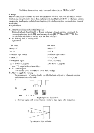
1. Multi-function watt-hour meter communication protocol DL/T 645-1997
1. Range
The standardization is used for the tariff device of multi-function watt-hour meter to do point to
point or one master to multi-slaves data exchange with hand-held unit(HHU) or other data terminal
equipments. It defines the technical specification of physical connection, communication link and
application.
4 Physical layer
………………………………………………….
4.1.6 Electrical characteristics of reading head
The reading head should be able to do data exchange with data terminal equipment. Its
communication interface is TTL level, or according to ITU-TV.24 and ITU-TV.28. The
electrical characteristics of reading head are shown in fig.4.
4.1.6.1 Working limit of reading head
Signal level
OFF status ON status
Binary “1” Binary “0”
MARK SPACE
Switch off light source Switch on light source
<-3V(V.28) >+3V(V.28)
<=0.8V(TTL input) >=2V(TTL input)
-0.5V~0.4V(TTL output) 2.4V~Up(TTL output)
Note: TTL negative logic is used here.
4.1.6.2 Transfer speed
Max transfer speed should be no lower than 2400bps.
4.1.7 Power supply for working
The power supply of reading head is provided by hand-held unit or other data terminal
equipment connected with it.
a)
0 1 0 1
(b)
ON 0 1 0 1
Fig.5 signal and modulation
a) electrical signal with no modulation b)infrared light signal after modulation
Fig.6 angle of light radiation
OFF
q
2. 4.2 Infrared light interface of modulation type
4.2.1 Modulation characteristics
The modulation of the signal is as Fig.5. The carrier frequency is 38kHz±1kHz
4.2.2 Optical characteristics
4.2.2.1 Reference temperature 23℃±2℃
4.2.2.2 Half-angle of light radiation q
q ³15° (as Fig.6)
4.2.2.3 Wave length
The wave length of infrared light is 900nm~1000nm
4.2.2.4 Emitter
The emitter produces infrared light with irradiance Ee/r ³50mW/m2 on the light axis 1m
away from the surface of emitter
4.2.2.5 Receiver
The irradiance Ee/r of the receiver on the light axis 10mm away from the surface of receiver
should satisfy following conditions:
Irradiance of infrared light Status of receiver
0.35mW/m2£Ee/r £20000mW/m2 ON
Ee/r £0.2mW/m2 OFF
4.2.2.6 Environment condition of the light
According to 4.1.5.4, the valid distance of communication is longer than 4m under the
environment.
4.2.3 Electrical characteristics
It's according to 4.1.6, but transfer speed should be no higher than 1200bps.
4.2.4 Use condition
4.2.4.1 It's should be avoided that strong light (sunlight and fluorescent light) directly irradiate the
receiving window of infrared light receiver.
4.2.4.2 It should be tried to keep the optical axis of the receiver consistent with that of the emitter
when working.
4.2.4.3 Avoid of appearing multiple consecutive“0” in the data.
4.3 Electrical interface of serial port RS-485
RS-485 is used by the standardization which make it's possible for multi-points connection. The
general performance of RS-485 interface should accord with following specification.
4.3.1 Electrostatic discharge (ESD) resistance of driver and receiver side is ±15V (human-body
model)
4.3.2 Common mode input voltage: -7V~+12V.
4.3.3 Differential mode input voltage: upper than 0.2V
4.3.4 Output voltage of driver: When the impedance of load is 54, the max output voltage of
driver is 5V and the min is 1.5V.
4.3.5 Tri-state output
4.3.6 Half-duplex communication mode
4.3.7 The driven capability should be no less than 32 interfaces of the same type
4.3.8 The valid distance of transfer should be no less than 1200m when the transfer speed is no
higher than 100kbps.
4.3.9 The bus is passive power. The tariff device or data terminal equipment provide isolation
power for it.
3. 5 Data-link layer
The protocol uses communication mode of master-slave structure and half-duplex. The
hand-held unit or other data terminal is master station and tariff device is salve station. Each tariff
device has its own address code. The creation and release of communication link is controlled by
the master station sending information frame. Each frame is composed of 7 parts including start
flag, address field of slave station, control code, data length, data field, check code of frame and end
flag, in which each part is composed of several bytes.
5.1 Byte format
Transfer direction
dDvdirection
D2 0 D0 D1 D3 D4 D5 D6 D7 P 1
Start bit Data of 8 bits Even check bit Stop bit
Fig.7 transfer sequence of byte
Instruction Code
Frame start flag 68H
Address field A0
A1
A2
A3
A4
A5
Frame start flag 68h
Control code C
Data length L
Data DATA
Check code CS
End flag 16H
Fig.8 Frame format
Each byte has 8 bits binary code. A start bi t (0), an even check bit and a stop bit are added when
transferring. So the total is 11 bits. The sequence of transfer is as Fig.7. The D0 is the LSB (least
significant bit) and D7 is the MSB (most significant bit). The transfer order is that the bit in
lower address is transferred first and then the bit in higher address.
5.2 Frame format
The frame is the basic unit for transferring information. The frame format is shown in fig.8.
4. 5.2.1 Frame start flag: indicate the start of one frame, its value is 68H=01101000B
5.2.2 Address field A0~A5: The address field comprises 6 bytes and each byte is composed of 2
BCD codes. It can express the address with 12 decimal digits at most. The address can be ID of
meter, or asset number, user number or device number, and so on which can be decided by users.
When the length of address is less than 6 bytes, the rest bytes can be filled with hexadecimal
number AAH. The lower address code is prior while higher one is in the latter. It's a broadcast
address when the address value is 999999999999H.
5.2.3 Control code: the format of control code is as following:
Function code
D7 D6 D5 D4 D3 D2 D1 D0
Flag of subsequent frame
Flag indicates whether slave station is abnormal
Transfer direction
D7=0: command frame from master station
D7=1: response frame from slave station
D6=0: slave station response correctly
D6=1: slave station response abnormally
D5=0: no subsequent data frame
D5=1: has subsequent data frame
D4~D0: function code of request and response
00000: reserved
00001: read data
00010: read subsequent data
00011: re-read data
00100: write data
01000: correcting time by broadcast
01010: write device address
01100: change communication speed
01111: change password
10000: clear maximum demand
5. 5.2.4 Data length L: L describes the bytes number of data field. L<=200 when reading data, L <=50
when writing data, and L=0 indicates no data.
5.2.5 Data field DATA: data field can be data identifier, data or password, etc whose structure
change with different control codes. The sender adds 33H to each byte when transferring while the
receiver subtract 33H from each byte when received.
5.2.6 Check code CS: It's the sum with modular operation on 256 of all bytes from the start flag to
the byte before check code namely it's binary arithmetic sum of each byte deducting overflowing
value over 256.
5.2.7 End flag 16H: indicates the end of the frame, its value is 16H=00010110B
5.3 Transfer
5.3.1 Front-leading bytes
To awaken the receiver, it should send FEH with 1~4 bytes before sending the frame.
5.3.2 Transfer order
All items in data field should be transferred with the order that the byte in lower position
should be transferred firstly and then the bytes in higher position.
For example, if power energy value is 123456.78kWh, the transfer order is as fig.9.
CS
AB 89 67 45 78 56 34 12
5.3.3 Transfer response
Each communication is initiated by master station with request command frame to slave station.
The requested slave station responses according to the request which is described by control
code in the command frame.
Td----Response delay after command frame 33H
is received: 20ms<=Td<=500ms
Tb----Pause time between bytes: Tb<=500ms
5.3.4 Error control
78 56 34 12 AB 89 67 45
....................................
5.3.5 Transfer speed
initial speed: 1200bps
standard speed: 300,600,1200,2400,4800,9600bps
special speed: defined by manufacturer
5.3.3 Response of transfer
33H
CS
Fig.9 Transfer order
Each communication starts from master station sending request command to slave station
which is selected according to address code in the frame. Then the slave station responses
according to the control code in command frame.
Response delay Td after command frame is received: 20ms£ Td£500ms
Pause time between bytes Tb: Tb£500ms
5.3.4 Error control
Byte check use even check method while frame check uses checksum of longitudinal bytes
in frame. The receiver should discard the frame and not response when even check or checksum
is wrong.
6. 6 Data identifier
6.1 Classification of data
Except measurement value, the counting value, happen time of max demand, instantaneous
voltage, electric current and power value are classified as variable; the calendar, time, user
setting value, characteristic word and status word of tariff device, tariff period are classified as
parametric variable.
6.2 Structure and code of data identifier
Tariff device stores all kinds of data with different types and attributes. The standardization
use four-layers tree structure to represent these data. It uses 4 fields in two bytes to represent
type and attribute of data respectively. These two bytes are DI1 and DI0 which is divided into
four fields DI1H, DI1L, DI0H and DI0L where DI0L is the least significant filed and DI1H is the most
significant field.
DI1H describes type of data and is shown as following:
DI1
DI1H DI1L
D7 D6 D5 D4 D3 D2 D1 D0
1001 power energy
1010 max demand
1011 variable
1100 parametric variable
1101 load curve
1110 user self defined
1111 reserved
DI1L, DI0H and DI0L describe different attributes of data. For the data of energy and max demand
which have multiple attributes such as attribute of time domain(current value, value of last
month, value of the month before last month), classification attribute(active, reactive), attribute
of power direction(positive, negative), tariff attribute( total amount, amount of different tariff)
and so on, their identifier is shown in 6.2.1 and 6.2.2.
6.2.1 Data identifier of energy
DI1
DI1H DI1L
D7 D6 D5 D4 D3 D2 D1 D0
1001 Energy 00 currently 00 active
01 last month 01 reactive
10 month before last month 10 reserved
11 collection 11 collection
DI0
DI0H DI0L
D7 D6 D5 D4 D3 D2 D1 D0
7. DI0
DI0H DI0L
D7 D6 D5 D4 D3 D2 D1 D0
0001 positive energy 0000 total energy
0010 negative energy 0001 tariff 1
0011 reactive power in 1st quadrant 0010 tariff 2
0100 reactive power in 4th quadrant ….
0101 reactive power in 2nd quadrant 1110 tariff k
0011 reactive power in 3rd quadrant 1111 collection of local data block
0111~1110 reserved
1111 collection
The coding of all data identifier of energy is shown in table A1.
6.2.2 Data identifier of max demand
DI1
DI1H DI1L
D7 D6 D5 D4 D3 D2 D1 D0
1010 max demand 00 currently 00 active
01 last month 01 reactive
10 month before last month 10 reserved
11 collection 11 collection
DI0
DI0H DI0L
D7 D6 D5 D4 D3 D2 D1 D0
0001 positive active max demand 0000 total energy
0010 negative active max demand 0001 tariff 1
0011 reactive power in 1st quadrant 0010 tariff 2
0100 reactive power in 4th quadrant ….
0101 reactive power in 2nd quadrant 1110 tariff k
0011 reactive power in 3rd quadrant 1111 collection of local data block
0111~1110 reserved
1111 collection
The coding of all data identifier of max demand is shown in table A2.
6.2.3 According to the data classification of the standardization, the happen time of max demand is
classified as variable. It is listed in table A3 individually which has same code but different type
symbol (A, B) with corresponding max demand considering the convenience for data terminal
reading data. The identifier codes of other data which are classified as variable and parametric
variable are listed in table A4, A5.
6.2.4 The identifier code of load record data block is listed in table A6.There is no definition about
the format and data length of this data in related standardization, so it can be self-defined by user.
6.3 Data set
6.3.1 Brief introduction
The identifier code of data represents single data item or collection of data items. A single data
8. item can be denoted uniquely by identifier code of corresponding data item in appendix A. The
identifier code of data block and data set can be used when requesting to access data set which
is composed of multiple data items.
6.3.2 Data item, data block and data set
6.3.2.1 Data item
They are some BCD codes which reflect a certain time-space value or digital value in tariff
device. For example, 9010H in NO. 1 in appendix A represents current positive active
energy whose format is XXXXXX.XX(kWh).
6.3.2.2 Data block
The data block is a group of data composed of continuous data items whose identifier fields
DI1H, DI1L, DI0H is same while DI0L is different (0,1,2,...,k(k is the possible maximum) in data
identifier. The identifier feature of data block is DI0L=1111B.
6.3.2.3 Data set A data set is composed of 1 or more data blocks. In data identifier, it is a data set
when DI1H, DI1L, DI0H is 1111B or 11B, which is composed of all possible value of the filed
and multiple data blocks in its next field. At this condition, no matter what value of its next
field is, it’s viewed as a data set identifier namely 11B or 1111B.
Then end flag of each data block which constitute the data set is AAH when
transferring. Tow continuous AAH represents a null data block. As Fig.10, the data set has
four data blocks in which data block 1 has m1 data and data block 2 has m2 data, data block
3 has no data, and data block 4 has m4 data,
Data block 1(m1)
AAH
Data block 2(m2)
AAH
AAH
AAH
Data block 3(0)
Data block 4(m4)
m1
m2
m3
m4
Fig.10 data set when transferring
6.3.3 Example of identifier of data set
a) identifier code DI1DI0=9010H(data item)
represents current positive active energy
b)identifier code DI1DI0=901FH(data block)
represents current positive total energy and the set of energy with all tariff (total energy,
energy of tariff 1, tariff 2, ....tariff k)
c)identifier code DI1DI0=90F0H(data set)
represents current positive and negative active energy. Is is make up of two items namely
9010H(current positive active energy) and 9020H(current negative active energy).
According to 6.3.2.3, the identifier is viewed as same with 90FFH.
d)identifier code DI1DI0=90FFH(data set)
9. represents the set of current positive and negative active energy which has 2(k+1) items
totally from 9010H to 902kH in table A1.
7 Application layer
7.1 Read data
7.1.1 Request frame from master station
function: request reading data
control code: C=01H
data length: L=02H
frame format:
68H A0 … A5 68H 01H 02H DI0 DI1 CS 16H
Data length
Control code
Identifier of data
7.1.2 Normally response from slave station
function: slave station response normally
control code: C=81H, no subsequent data frame
C=A1H, has subsequent data frame
data length: L=02H+m(data length)
format of no subsequent data frame:
68H A0 … A5 68H 81H L DI0 DI1 N1 … Nm CS 16H
format of has subsequent data frame:
Data identifier
Data length
Control code
68H A0 … A5 68H C1H 01H ERR CS 16H
7.1.3 Salve station response abnormally
function: slave station receives wrong request or no corresponding data
control code: C=C1H
data length: L=01H
frame format:
Data item
10. 68H A0 … A5 68H C1H 01H ERR CS 16H
Note: for error information word, please refer appendix B5.
7.2 Read subsequent data
7.2.1 Request frame from master station
function: request reading subsequent data
control code: C=02H
data length: L=02H
frame format:
68H A0 … A5 68H 02H 02H DI0 DI1 CS 16H
7.2.2 Slave station response normally
function: subsequent data is transferred according to the format of normal data frame
control code: C=82H, no subsequent data frame
C=A2H, has subsequent data frame
data length: L=02H+m(data length)
format of no subsequent data frame :
68H A0 … A5 68H 82H L DI0 DI1 N1 … Nm CS 16H
format of has subsequent data frame:
68H A0 … A5 68H A2H L DI0 DI1 N1 … Nm CS 16H
7.2.3 Salve station response abnormally
function: slave station receives wrong request or no corresponding data
control code: C=C2H
data length: L=01H
frame format:
68H A0 … A5 68H C2H 01H ERR CS 16H
7.3 Re-read data
7.3.1 Request frame from master station
function: request slave station re-transferring the data in last frame
control code: C=03H
data length: L=00H
frame format:
68H A0 … A5 68H 03H 00H CS 16H
7.3.2 Slave station response normally
control code: C=83H, no subsequent frame
C=A3H, has subsequent frame
data length: L=02H+m(data length)
Error information word
11. format of no subsequent frame :
68H A0 … A5 68H 83H L DI0 DI1 N1 … Nm CS 16H
format of has subsequent frame:
68H A0 … A5 68H A3H L DI0 DI1 N1 … Nm CS 16H
7.3.3 Salve station response abnormally
control code: C=C3H
data length: L=01H
frame format:
68H A0 … A5 68H C3H 01H ERR CS 16H
7.4 Write data
7.4.1 Request frame for writing data
function: master station requests slave station to set data(or program)
control code: C=04H
data length: L=02H+m(data length)
frame format:
68H A0 … A5 68H 04H L DI0 DI1 N1 … Nm CS 16H
7.4.2 Slave station response normally
function: slave station notify the executing result of the request to master station
control code: C=84H
data length: L=00H
frame format
68H A0 … A5 68H 84H 00H CS 16H
7.4.3 Salve station response abnormally
control code: C=C4H
data length: L=01H
frame format:
68H A0 … A5 68H C4H 01H ERR CS 16H
7.5 Correcting time with broadcast
function: make the time of slave station is synchronous with master slave
control code: C=08H
data length: L=06H
data field: YYMMDDhhmmss (year.month.day.hour.minute.second)
frame format:
68H 99H … 99H 68H 08H 06H ss mm hh
DD MM YY CS 16H
1. It doesn't need response for correcting time with broadcast
12. 2.Only when the time difference between slave station and master station is under ±5min, it
executes correcting time command by setting the time of slave station same with that in the
command.
3. It doesn't recommend correcting time at 0 clock in case that it will affect some regular
operations at 0 clock.
4. It allows correcting time only once every day.
7.6 Write address of device
7.6.1 Request for write address of device
function: set address code for some slave station
control code: C=0AH
address field: 99...99H
data length: L=06H
data field: A0...A5 (address code of device)
frame format
68H 99H … 99H 68H 0AH 06H A0 … A5 CS 16H
Note: The request uses broadcast address, which requires the slave station that is set address has
corresponding key (switcher) cooperating with the command. The slave station whose key is
pressed during the period of master station broadcasting request will response, others will not
response.
7.6.2 Slave station response normally
function: the device which execute the request correctly responses
control code: C=8AH
address field: A0...A5 (new address code of the device)
data length: L=00H
frame format
68H A0 … A5 68H 8AH 00H CS 16H
7.7 change communication speed
7.7.1 request for changing communication speed
function: request new communication speed other than 1200bps
control code: C=0CH
data length: L=01H
frame format:
68H A0 … A5 68H 8CH 01H Z CS 16H
7.7.2 salve station response with confirmation
Feature word of speed
function: slave station confirms the request of changing communication speed
control code: C=8CH
data length: L=01H
13. frame format:
7.7.3 Slave station deny the request of changing communication speed
68H A0 … A5 68H 8CH 01H Z CS 16H
control code: C=8CH
data length: L=01H
data field: Z=FFH, represent deny
frame format:
Same with feature word in request
speed
68H A0 … A5 68H 8CH 01H FFH CS 16H
7.8 change password
7.8.1 Request for changing password
function: change current password of slave station
control code:C=0FH
data length:L=08H
data field: PAoP0oP1oP2oPANP0NP1NP2N
frame format:
68H A0 … A5 68H 0FH 08H PAo P0o P1o P2o PAN P0N P1N P2N CS 16H
P0oP1oP2o is original password or password with higher authority. PAo represent authority of the
password; P0NP1NP2N represents new password or password that need be set.
PAN is the authority of new password. The data range of PAo,PAN is 0~9 which 0 is the
highest authority. The number is larger while the authority is lower. The level of authority is divided
into highest, programming and clear max demand.
7.8.2 Slave station response normally
function: slave station notify changing password correctly
control code: C=8FH
data length: L=04H
data field: authority of password and password PANP0NP1NP2N
frame format:
68H A0 … A5 68H 8FH 04H PAN P0N P1N P2N CS 16H
7.8.3 slave station doesn't response when it go wrong
7.9 Clear max demand
7.9.1 request for clearing max demand
function: for tariff device which is working on non-automatically meter reading mode, the
command can implement clearing max demand and data rolling of energy in current month, last
month, the month before last month and register of max demand.
Control code:C=10H
data length: L=00H
frame format:
68H A0 … A5 68H 10H 00H CS 16H