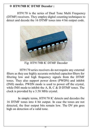
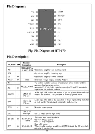
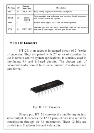
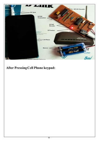
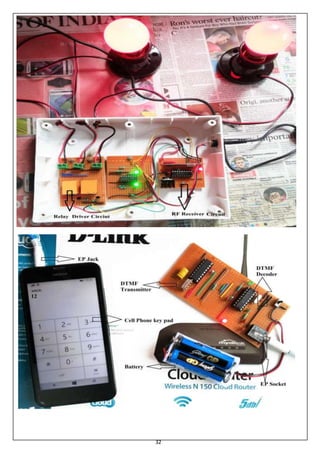
1
Cell Phone Controlled Home Automation
System using DTMF Technology
Thesis submitted in partial fulfilment of the
requirements for the Degree of Bachelor of Technology
in Electronics & Communication Engineering
2012-2016
Submitted by
Name Roll No
Taufique Sekh 28000312018
Under the guidance of
Prof. Shabana Huda, Asst. Prof.
DEPARTMENT OF ELECTRONICS & COMMUNICATION ENGINEERING
Camellia Institute of Engineering
Affiliated to
Maulana Abul Kalam Azad University of Technology
(Formerly known as West Bengal University of Technology)
2
Contents
Topic Name Page No
 ABSTRACT 1-2
 THEORY 3-5
 CIRCUIT PRINCIPLE 6-7
 CIRCUIT COMPONENTS 8-19
 BUDGETARY ESTIMATION 20-21
 CIRCUIT DESIGN AND CIRCUIT OPERATION 22-26
 RESULTS 27-29
 ADVANTAGES AND LIMITATIONS 30-31
 CONCLUSION 32-33
 FUTURE SCOPE 34-35
 REFERENCES 36-37
3
Chapter 1
ABSTRACT
4
Abstract:
Generally, appliancesused in our home are controlledwith
the help of switches. These days, we can see automation of
these appliances using many technologies. This project
presents the controlling of home appliances using DTMF
technology.
This home appliancescontrol or home automation project
uses DTMF decoder circuit to control home and
office electrical appliances. Just connect your cell phone
headset (headphone)jack to the mobile phone and then mobile
will control electrical appliances and electrical equipment
through the DTMF key pad of your cell phone. Here for
demonstrating, we are controlling an electrical bulb using this
circuit project but you can extend this circuit to control many
electrical devices with some modifications using4×16 decoder
IC.
5
Chapter 2
THEORY
6
Theory:
DTMF is acronym for Dual Tone Multi Frequency. So, just
think when we make call for customer care, they will ask you
to press 1, 2 or any other number. When we press a number
from our mobile, one particular action is happening. All this is
because of DTMF. When a button is pressed in our mobile
keypad, it will generate a tone of two frequencies. These tones
are called row and column frequencies.
Generally, row frequencies are low frequencies and column
frequencies are high frequencies. These frequencies for DTMF
are chosen in such a way that they don’t have harmonic
relation with the others, so that they will not produce same
tones. The column frequencies are slightly louder than the row
frequencies to compensate for the high-frequency roll off of
voice audio systems.
We have learned that each button pressed in keypad will
produce a tone which differs from others. Now we should use
these tones for our appliances. So this DTMF encoder is
present in mobile. Output from keypad can be converted into
digital form using DTMF decoder IC HT9107B.
7
Table showing DTMF Low and High frequency tones and
decoded output:
8
Chapter 3
CIRCIUT PRINCIPLE
9
DTMF Controlled Home Appliances Circuit Principle:
The main principle of this circuit is to control appliances like
light and fan using DTMF technology. DTMF encoder is
present in our mobile and decoderis HT9107BIC. Mobile jack
is connected at 1nf capacitor. Mobilejack consists of two wires
(Red and black). Red wire is connected to the decoder IC and
Black is grounded. When a button is pressed from mobile it
generates a tone which is decoded by the decoder IC and it is
sent to the HT12E encoder chip and this signal is fed to TX
433MHz transmitter module which is transmit the DTMF
signal and this signal is received by RX433 MHz Receiver
module. Receiver module is connected to the Decoder chip
HT12D which is decoding the signal to convert binary format.
When we press any key in the remote, the transmitter section
generates the corresponding RF signal and this signal is
received by the receiver section, hence it switches the
corresponding appliance.
10
Chapter 4
CIRCUIT
COMPONENTS
11
Circuit Components:
This circuit mainly consists of the following components.
 HT9170B IC DTMF Decoder
 HT12E Encoder
 HT12D Decoder
 CD4013 D Flip-Flop
 Relay Driver Stage
 Resistors – R1, R2 and R3
 Capacitors – C1, C2, C3 and C4
 Crystal Oscillator X1, 3.57MHz
 RX and TX Module 433 MHz
 BC547B Transistor
12
 HT9170B IC DTMF Decoder :
HT9170 is the series of Dual Tone Multi Frequency
(DTMF) receivers. They employ digital counting techniques to
detect and decode the 16 DTMF tones into 4 bit output code.
Fig: HT9170B IC DTMF Decoder
HT9170 series receivers do not require any external
filters as they use highly accurate switched capacitor filters for
filtering low and high frequency signals from the DTMF
tones. They also support power down (PWDN) and inhibit
(INH) modes. PWDN mode is used to power off the crystal,
while INH mode to inhibit the A, B, C & D DTMF tones. The
clock is provided by a 3.58 MHz crystal.
In simple terms, HT9170 IC detects and decodes the
16 DTMF tones into 4 bit output. In case the tones are not
detected, the four output bits remain low. The DV pin goes
high on detection of a valid tone.
13
Pin Diagram :
Fig: Pin Diagram of HT9170
Pin Description:
Pin Name I/O
Internal
Connection Description
VP I
OPERATIONA
L AMPLIFIER Operational amplifier non-inverting input
VN I Operational amplifier inverting input
GS O Operational amplifier output terminal
VREF O VREF Reference voltage output, normally VDD/2
X1 I
OSCILLATOR
The system oscillator consists of an inverter, a bias resistor and the
necessary load capacitor on chip.
A standard 3.579545MHz crystal connected to X1 and X2 ter- minals
implements the oscillator function.
X2 O
PWDN I CMOS IN
Pull-low
Active high. This enables the device to go into power down mode and
inhibits the oscillator. This pin input is internally pulled down.
INH I CMOS IN
Pull-low
Logic high. This inhibits the detection of tones representing characters
A, B, C and D. This pin input is internally pulled down.
VSS -- ---- Negative power supply
OE I
CMOS IN
Pull-high D0~D3 output enable, high active
D0~D3 O CMOS OUT
Tristate
Receiving data output terminals
OE=”H”: Output enable
OE=”L”: High impedance
DV O CMOS OUT
Data valid output
When the chip receives a valid tone (DTMF) signal, the DV goes high;
otherwise it remains low.
14
Pin Name I/O
Internal
Connection Description
EST O CMOS OUT Early steering output (see Functional Description)
RT/GT I/O CMOS
IN/OUT
Tone acquisition time and release time can be set through connection
with external resistor and capacitor.
VDD --- ----- Positive power supply, 2.5V~5.5V for normal operation
DVB O CMOS OUT
One-shot type data valid output, normal high, when the chip receives a
valid time (DTMF) signal, the DVB goes low for 10ms.
 HT12EEncoder :
HT12E is an encoder integrated circuit of 212
series
of encoders. They are paired with 212
series of decoders for
use in remote control system applications. It is mainly used in
interfacing RF and infrared circuits. The chosen pair of
encoder/decoder should have same number of addresses and
data format.
Fig: HT12E Encoder
Simply put, HT12E converts the parallel inputs into
serial output. It encodes the 12 bit parallel data into serial for
transmission through an RF transmitter. These 12 bits are
divided into 8 address bits and 4 data bits.
15
HT12E has a transmission enable pin which is active
low. When a trigger signal is received on TE pin, the
programmed addresses/data are transmitted together with the
header bits via an RF or an infrared transmission medium.
HT12E begins a 4-word transmission cycle upon receipt of a
transmission enable. This cycle is repeated as long as TE is
kept low. As soon as TE returns to high, the encoder output
completes its final cycle and then stops.
Pin Diagram:
Fig: Pin Diagram of HT12E
16
Pin Description:
Pin No Function Name
1
8 bit Address pins for input
A0
2 A1
3 A2
4 A3
5 A4
6 A5
7 A6
8 A7
9 Ground (0V) Ground
10
4 bit Data/Address pins for input
AD0
11 AD1
12 AD2
13 AD3
14 Transmission enable; active low TE
15 Oscillator input Osc2
16 Oscillator output Osc1
17 Serial data output Output
18 Supply voltage; 5V (2.4V-12V) Vcc
17
HT12D Decoder:
HT12D is a decoder integrated circuit that
belongs to 212
series of decoders. This series of decoders are
mainly used for remote control system applications, like
burglar alarm, car door controller, security system etc. It is
mainly provided to interface RF and infrared circuits. They
are paired with 212
series of encoders. The chosen pair of
encoder/decoder should have same number of addresses and
data format.
Fig: HT12D Encoder
In simple terms, HT12D converts the serial input into
parallel outputs. It decodes the serial addresses and data
received by, say, an RF receiver, into parallel data and sends
them to output data pins. The serial input data is compared
with the local addresses three times continuously. The input
data code is decoded when no error or unmatched codes are
found. A valid transmission in indicated by a high signal at
VT pin.
HT12D is capable of decoding 12 bits, of which 8 are address
bits and 4 are data bits. The data on 4 bit latch type outputpins
remain unchanged until new is received.
18
Pin Diagram:
Fig: Pin Diagram of HT12D
Pin Description:
Pin No Function Name
1
8 bit Address pins for input
A0
2 A1
3 A2
4 A3
5 A4
6 A5
7 A6
8 A7
9 Ground (0V) Ground
10
4 bit Data/Address pins for output
D0
11 D1
12 D2
13 D3
14 Serial data input Input
15 Oscillator output Osc2
16 Oscillator input Osc1
17 Valid transmission; active high VT
19
18 Supply voltage; 5V (2.4V-12V) Vcc
ASK RF RX and TX Module :
The RF module, as the name suggests,
operates at Radio Frequency. The corresponding frequency
range varies between 30 kHz & 300 GHz. In this RF system,
the digital data is represented as variations in the amplitude of
carrier wave. This kind of modulation is known as Amplitude
Shift Keying (ASK).
Fig: ASK RF RX and TX Module
Transmission through RF is better than IR (infrared) because
of many reasons. Firstly, signals through RF can travel
through larger distances making it suitable for long range
applications. Also, while IR mostly operates in line-of-sight
mode, RF signals can travel even when there is an obstruction
between transmitter & receiver. Next, RF transmission is more
strong and reliable than IR transmission. RF communication
uses a specific frequency unlike IR signals which are affected
by other IR emitting sources.
20
This RF module comprises of an RF Transmitter and an RF
Receiver. The transmitter/receiver (Tx/Rx) pair operates at a
frequency of 434 MHz. An RF transmitter receives serial data
and transmits it wirelessly through RF through its antenna
connected at pin4. The transmission occurs at the rate of
1Kbps - 10Kbps.The transmitted data is received by an RF
receiver operating at the same frequency as that of the
transmitter.
The RF module is often used along with a pair of
encoder/decoder. The encoder is used for encoding parallel
data for transmission feed while reception is decoded by a
decoder. HT12E-HT12D, HT640-HT648, etc. are some
commonly used encoder/decoder pair ICs.
Pin Diagram:
21
Pin Description:
RF Transmitter
Pin No Function Name
1 Ground (0V) Ground
2 Serial data input pin Data
3 Supply voltage; 5V Vcc
4 Antenna output pin ANT
RF Receiver
Pin No Function Name
1 Ground (0V) Ground
2 Serial data output pin Data
3 Linear output pin; not connected NC
4 Supply voltage; 5V Vcc
5 Supply voltage; 5V Vcc
6 Ground (0V) Ground
7 Ground (0V) Ground
8 Antenna input pin ANT
22
Chapter 5
BUDGETARY
ESTIMATION
23
BUDGETARY ESTIMATION:
Sl.No Component Rate(Rs.) Quantity Amount(Rs.)
1 HT9107B IC DTMF
Decoder
25 1 25
2 HT12E Encoder 30 1 30
3 HT12D Decoder 30 1 30
4 Relay Driver Stage 50 2 100
5 Resistors – R1, R2
and R3
.50 6 3
6 Capacitors – C1, C2,
C3,C4 and C5
.50 5 2.5
7 Crystal Oscillator X1,
3.57MHz
5 1 5
8 RX and TX Module
433 MH
250 1 250
9 Bulb + Holder+Plug 75 1 75
10 Cabinet 100 1 100
11 12V SMPS 2A 400 1 400
12 EP Jack 10 1 10
13 Battery 10 2 20
14 EP Socket 5 1 5
15 IC Vero Board 20 3 60
16 CD4013 13 2 26
17 BC547B 3 2 6
18 Connecting wires 30 --- 30
Total Amount 1,177.50
24
Chapter 6
Circuit Design
&
Circuit Operation
25
Circuit Design of DTMF Controlled Home Appliances:
IC HT9107B DTMF Decoder:
The decoder IC consists of an inbuilt operational Amplifier.
The outputof op-amp is given to the pre-filters to separate low
and high frequencies. Then it is passed through frequency and
code detector circuits, thus 4-bit binary code is latched.
Tone from mobile is sent to op-amp through series of resistor
(100 kilo-Ohm) and capacitor (1nf). Pin1 of DTMF IC i.e. non
inverting pin is connected to pin4 i.e. Vref. Pin3 is the output
of operational amplifier which is feedback to pin2 using 100
kilo-Ohm resistor. 7 and 8 pins are connected to crystal
oscillatorof frequency 3.579545MHz. 15th
pin is data valid pin
it becomes high when DTMF toneis detected else remains low.
The process of frequency detection to digitalization of the
signal is done by steering circuit consisting of EST, RT/GT,
and resistor (10k), capacitor. Pins 11 to 14 producethe decoded
output.
26
DTMF Transmitter and Receiver using RF Module:
27
HT12E EncoderIC will convert the 4 bit parallel data given to
pins D0 – D3 to serial data and will be available at DOUT.
This output serial data is given to ASK RF Transmitter.
Address inputs A0 – A7 can be used to provide data security
and can be connected to GND (Logic ZERO) or left open
(Logic ONE). Status of these Address pins should match with
status of address pins in the receiver for the transmission of the
data. Data will be transmitted only when the Transmit Enable
pin (TE) is LOW. 33k resistor will provide the necessary
external resistance for the operation of the internal oscillator of
HT12E.
RF Receiver receives the data transmitted using RF
Transmitter. HT12D decoder will convert the received serial
data to 4 bit parallel data D0 – D3. The status of these address
pins A0-A7 should match with status of address pin in the
HT12E at the transmitter for the transmission of data. The LED
connected to the above circuit glows when valid data
transmission occurs from transmitter to receiver. 750KΩ
resistor will provide the necessary resistance required for the
internal oscillator of the HT12D.
28
Relay Driver Circuit:
As per the specifications of the IC, its outputs
correspondingly switch ON and OFF in accordance with the
DTMF tones generated and transmitted by the transmitter
stage. The above switching of the outputs of HT12D IC is
integrated to 4 discretely configured IC 4013 based flip flop
stages which respond by toggling the attached relay driver
stages. The relays can be wired to the relevant loads for
achieving the intended switching via the DTMF transmitter
handset. The outputof flip flop is connected to the relay driver
circuit via 1KΩ resistor; this output energizes the relay coil
through BC547 transistor and turns ON the bulb that is
connected at the normally open terminal of relay circuit.
29
Chapter 7
Results
30
Before Pressing Cell Phone keypad:
31
After PressingCell Phone keypad:
32
33
Chapter 8
ADVANTAGES
&
LIMITATIONS
34
Advantages of DTMF ControlledHomeAutomationSystem
Circuit:
1. One can control home appliances from anywhere.
2. It reduces wastage of electricity when we forgot to
switch off the lights & fans and gone outside.
3. It is very low cost compared to other technologies like
GSM.
Limitations of DTMF Controlled Home Appliances:
1. Number of appliances is limited as our mobile can
generate only 16 tones.
35
Chapter 9
CONCLUSION
36
Conclusion:
Mobile phones have become an indispensable part of our life.
Our system uses a controller and a cellular phone for its
operations. The systems can be used as a test bed for any
application that requires on-off switching based applications.
Wireless controlled home appliances in the comforts of any
environment will revolutionize our way of living.
37
Chapter 10
FUTURE SCOPE
38
FUTURESCOPE:
1) Possibility of confirming the devices initial condition
(status) using short messaging system(SMS)
2) Though mobile in the control panel required to be
charged, therefore charging system should be automated which
meant a timer can be implemented so that mobile can be
charged after a certain period and disconnected from the
charger when not required.
3) The system can be expanded to provide such control
over the GPRS. In this way, the capabilities of the internet can
be combined with the capabilities of our physical line free
communication system. Furthermore, by adding a closed loop
control facility, the system capabilities can be improved.
39
Chapter 11
REFERENCES
40
REFERENCES:
[1] GSM SYSTEM SURVEY ,Student text, EN/LZT 1233321,
R5B revised upgrade edition. p. 192.
[2] Dual-tone multi-frequency, Available:
http://en.wikipedia.org/wiki/Dual-tone_multi-frequency
[3] Schenker, L., “Pushbutton Calling with a Two-Group
Voice-Frequency Code” - The Bell system technical journal
(ISSN 0005-8580) vol:39 iss:1 pp:235-255, 1960
[4] DTMF decoding, Available:
http://www.dattalo.com/technical/theory/dtmf.html
[5] “Microcontroller Technology:16F84A”, prentice hall , 7th
edition, page32, 2002
[6] I. Coskun and H. Ardam, “A Remote Controller for Home
and Office Appliances by Telephone”, IEEE Trans. Consumer
Electron. , vol. 44, no. 4, pp. 1291- 1297, November 1998
[7] PIC16F84A microcontroller data sheet, Available:
http://ww1.microchip.com/downloads/en/devicedoc/35007b.pd
f
[8] Daldal Nihat, “GSM Based Security and Control System”
(In Turkish), M.Sc. Term Project, Gazi University, Ankara,
2003.
[9] E. Wong, “A Phone-Based Remote Controller For Home
And Office Automation”, IEEE Trans.Consumer Electron. ,
vol. 40, no. 1, pp. 28-33, February 1995.
[10] Relay Information, Available:
http://en.wikipedia.org/wiki/Relay
41
THE END
For contact ,visit:: http://taufiquesekh.strikingly.com

Cell Phone Controlled Home Automation System using DTMF Technology

  • 1.
    1 Cell Phone ControlledHome Automation System using DTMF Technology Thesis submitted in partial fulfilment of the requirements for the Degree of Bachelor of Technology in Electronics & Communication Engineering 2012-2016 Submitted by Name Roll No Taufique Sekh 28000312018 Under the guidance of Prof. Shabana Huda, Asst. Prof. DEPARTMENT OF ELECTRONICS & COMMUNICATION ENGINEERING Camellia Institute of Engineering Affiliated to Maulana Abul Kalam Azad University of Technology (Formerly known as West Bengal University of Technology)
  • 2.
    2 Contents Topic Name PageNo  ABSTRACT 1-2  THEORY 3-5  CIRCUIT PRINCIPLE 6-7  CIRCUIT COMPONENTS 8-19  BUDGETARY ESTIMATION 20-21  CIRCUIT DESIGN AND CIRCUIT OPERATION 22-26  RESULTS 27-29  ADVANTAGES AND LIMITATIONS 30-31  CONCLUSION 32-33  FUTURE SCOPE 34-35  REFERENCES 36-37
  • 3.
  • 4.
    4 Abstract: Generally, appliancesused inour home are controlledwith the help of switches. These days, we can see automation of these appliances using many technologies. This project presents the controlling of home appliances using DTMF technology. This home appliancescontrol or home automation project uses DTMF decoder circuit to control home and office electrical appliances. Just connect your cell phone headset (headphone)jack to the mobile phone and then mobile will control electrical appliances and electrical equipment through the DTMF key pad of your cell phone. Here for demonstrating, we are controlling an electrical bulb using this circuit project but you can extend this circuit to control many electrical devices with some modifications using4×16 decoder IC.
  • 5.
  • 6.
    6 Theory: DTMF is acronymfor Dual Tone Multi Frequency. So, just think when we make call for customer care, they will ask you to press 1, 2 or any other number. When we press a number from our mobile, one particular action is happening. All this is because of DTMF. When a button is pressed in our mobile keypad, it will generate a tone of two frequencies. These tones are called row and column frequencies. Generally, row frequencies are low frequencies and column frequencies are high frequencies. These frequencies for DTMF are chosen in such a way that they don’t have harmonic relation with the others, so that they will not produce same tones. The column frequencies are slightly louder than the row frequencies to compensate for the high-frequency roll off of voice audio systems. We have learned that each button pressed in keypad will produce a tone which differs from others. Now we should use these tones for our appliances. So this DTMF encoder is present in mobile. Output from keypad can be converted into digital form using DTMF decoder IC HT9107B.
  • 7.
    7 Table showing DTMFLow and High frequency tones and decoded output:
  • 8.
  • 9.
    9 DTMF Controlled HomeAppliances Circuit Principle: The main principle of this circuit is to control appliances like light and fan using DTMF technology. DTMF encoder is present in our mobile and decoderis HT9107BIC. Mobile jack is connected at 1nf capacitor. Mobilejack consists of two wires (Red and black). Red wire is connected to the decoder IC and Black is grounded. When a button is pressed from mobile it generates a tone which is decoded by the decoder IC and it is sent to the HT12E encoder chip and this signal is fed to TX 433MHz transmitter module which is transmit the DTMF signal and this signal is received by RX433 MHz Receiver module. Receiver module is connected to the Decoder chip HT12D which is decoding the signal to convert binary format. When we press any key in the remote, the transmitter section generates the corresponding RF signal and this signal is received by the receiver section, hence it switches the corresponding appliance.
  • 10.
  • 11.
    11 Circuit Components: This circuitmainly consists of the following components.  HT9170B IC DTMF Decoder  HT12E Encoder  HT12D Decoder  CD4013 D Flip-Flop  Relay Driver Stage  Resistors – R1, R2 and R3  Capacitors – C1, C2, C3 and C4  Crystal Oscillator X1, 3.57MHz  RX and TX Module 433 MHz  BC547B Transistor
  • 12.
    12  HT9170B ICDTMF Decoder : HT9170 is the series of Dual Tone Multi Frequency (DTMF) receivers. They employ digital counting techniques to detect and decode the 16 DTMF tones into 4 bit output code. Fig: HT9170B IC DTMF Decoder HT9170 series receivers do not require any external filters as they use highly accurate switched capacitor filters for filtering low and high frequency signals from the DTMF tones. They also support power down (PWDN) and inhibit (INH) modes. PWDN mode is used to power off the crystal, while INH mode to inhibit the A, B, C & D DTMF tones. The clock is provided by a 3.58 MHz crystal. In simple terms, HT9170 IC detects and decodes the 16 DTMF tones into 4 bit output. In case the tones are not detected, the four output bits remain low. The DV pin goes high on detection of a valid tone.
  • 13.
    13 Pin Diagram : Fig:Pin Diagram of HT9170 Pin Description: Pin Name I/O Internal Connection Description VP I OPERATIONA L AMPLIFIER Operational amplifier non-inverting input VN I Operational amplifier inverting input GS O Operational amplifier output terminal VREF O VREF Reference voltage output, normally VDD/2 X1 I OSCILLATOR The system oscillator consists of an inverter, a bias resistor and the necessary load capacitor on chip. A standard 3.579545MHz crystal connected to X1 and X2 ter- minals implements the oscillator function. X2 O PWDN I CMOS IN Pull-low Active high. This enables the device to go into power down mode and inhibits the oscillator. This pin input is internally pulled down. INH I CMOS IN Pull-low Logic high. This inhibits the detection of tones representing characters A, B, C and D. This pin input is internally pulled down. VSS -- ---- Negative power supply OE I CMOS IN Pull-high D0~D3 output enable, high active D0~D3 O CMOS OUT Tristate Receiving data output terminals OE=”H”: Output enable OE=”L”: High impedance DV O CMOS OUT Data valid output When the chip receives a valid tone (DTMF) signal, the DV goes high; otherwise it remains low.
  • 14.
    14 Pin Name I/O Internal ConnectionDescription EST O CMOS OUT Early steering output (see Functional Description) RT/GT I/O CMOS IN/OUT Tone acquisition time and release time can be set through connection with external resistor and capacitor. VDD --- ----- Positive power supply, 2.5V~5.5V for normal operation DVB O CMOS OUT One-shot type data valid output, normal high, when the chip receives a valid time (DTMF) signal, the DVB goes low for 10ms.  HT12EEncoder : HT12E is an encoder integrated circuit of 212 series of encoders. They are paired with 212 series of decoders for use in remote control system applications. It is mainly used in interfacing RF and infrared circuits. The chosen pair of encoder/decoder should have same number of addresses and data format. Fig: HT12E Encoder Simply put, HT12E converts the parallel inputs into serial output. It encodes the 12 bit parallel data into serial for transmission through an RF transmitter. These 12 bits are divided into 8 address bits and 4 data bits.
  • 15.
    15 HT12E has atransmission enable pin which is active low. When a trigger signal is received on TE pin, the programmed addresses/data are transmitted together with the header bits via an RF or an infrared transmission medium. HT12E begins a 4-word transmission cycle upon receipt of a transmission enable. This cycle is repeated as long as TE is kept low. As soon as TE returns to high, the encoder output completes its final cycle and then stops. Pin Diagram: Fig: Pin Diagram of HT12E
  • 16.
    16 Pin Description: Pin NoFunction Name 1 8 bit Address pins for input A0 2 A1 3 A2 4 A3 5 A4 6 A5 7 A6 8 A7 9 Ground (0V) Ground 10 4 bit Data/Address pins for input AD0 11 AD1 12 AD2 13 AD3 14 Transmission enable; active low TE 15 Oscillator input Osc2 16 Oscillator output Osc1 17 Serial data output Output 18 Supply voltage; 5V (2.4V-12V) Vcc
  • 17.
    17 HT12D Decoder: HT12D isa decoder integrated circuit that belongs to 212 series of decoders. This series of decoders are mainly used for remote control system applications, like burglar alarm, car door controller, security system etc. It is mainly provided to interface RF and infrared circuits. They are paired with 212 series of encoders. The chosen pair of encoder/decoder should have same number of addresses and data format. Fig: HT12D Encoder In simple terms, HT12D converts the serial input into parallel outputs. It decodes the serial addresses and data received by, say, an RF receiver, into parallel data and sends them to output data pins. The serial input data is compared with the local addresses three times continuously. The input data code is decoded when no error or unmatched codes are found. A valid transmission in indicated by a high signal at VT pin. HT12D is capable of decoding 12 bits, of which 8 are address bits and 4 are data bits. The data on 4 bit latch type outputpins remain unchanged until new is received.
  • 18.
    18 Pin Diagram: Fig: PinDiagram of HT12D Pin Description: Pin No Function Name 1 8 bit Address pins for input A0 2 A1 3 A2 4 A3 5 A4 6 A5 7 A6 8 A7 9 Ground (0V) Ground 10 4 bit Data/Address pins for output D0 11 D1 12 D2 13 D3 14 Serial data input Input 15 Oscillator output Osc2 16 Oscillator input Osc1 17 Valid transmission; active high VT
  • 19.
    19 18 Supply voltage;5V (2.4V-12V) Vcc ASK RF RX and TX Module : The RF module, as the name suggests, operates at Radio Frequency. The corresponding frequency range varies between 30 kHz & 300 GHz. In this RF system, the digital data is represented as variations in the amplitude of carrier wave. This kind of modulation is known as Amplitude Shift Keying (ASK). Fig: ASK RF RX and TX Module Transmission through RF is better than IR (infrared) because of many reasons. Firstly, signals through RF can travel through larger distances making it suitable for long range applications. Also, while IR mostly operates in line-of-sight mode, RF signals can travel even when there is an obstruction between transmitter & receiver. Next, RF transmission is more strong and reliable than IR transmission. RF communication uses a specific frequency unlike IR signals which are affected by other IR emitting sources.
  • 20.
    20 This RF modulecomprises of an RF Transmitter and an RF Receiver. The transmitter/receiver (Tx/Rx) pair operates at a frequency of 434 MHz. An RF transmitter receives serial data and transmits it wirelessly through RF through its antenna connected at pin4. The transmission occurs at the rate of 1Kbps - 10Kbps.The transmitted data is received by an RF receiver operating at the same frequency as that of the transmitter. The RF module is often used along with a pair of encoder/decoder. The encoder is used for encoding parallel data for transmission feed while reception is decoded by a decoder. HT12E-HT12D, HT640-HT648, etc. are some commonly used encoder/decoder pair ICs. Pin Diagram:
  • 21.
    21 Pin Description: RF Transmitter PinNo Function Name 1 Ground (0V) Ground 2 Serial data input pin Data 3 Supply voltage; 5V Vcc 4 Antenna output pin ANT RF Receiver Pin No Function Name 1 Ground (0V) Ground 2 Serial data output pin Data 3 Linear output pin; not connected NC 4 Supply voltage; 5V Vcc 5 Supply voltage; 5V Vcc 6 Ground (0V) Ground 7 Ground (0V) Ground 8 Antenna input pin ANT
  • 22.
  • 23.
    23 BUDGETARY ESTIMATION: Sl.No ComponentRate(Rs.) Quantity Amount(Rs.) 1 HT9107B IC DTMF Decoder 25 1 25 2 HT12E Encoder 30 1 30 3 HT12D Decoder 30 1 30 4 Relay Driver Stage 50 2 100 5 Resistors – R1, R2 and R3 .50 6 3 6 Capacitors – C1, C2, C3,C4 and C5 .50 5 2.5 7 Crystal Oscillator X1, 3.57MHz 5 1 5 8 RX and TX Module 433 MH 250 1 250 9 Bulb + Holder+Plug 75 1 75 10 Cabinet 100 1 100 11 12V SMPS 2A 400 1 400 12 EP Jack 10 1 10 13 Battery 10 2 20 14 EP Socket 5 1 5 15 IC Vero Board 20 3 60 16 CD4013 13 2 26 17 BC547B 3 2 6 18 Connecting wires 30 --- 30 Total Amount 1,177.50
  • 24.
  • 25.
    25 Circuit Design ofDTMF Controlled Home Appliances: IC HT9107B DTMF Decoder: The decoder IC consists of an inbuilt operational Amplifier. The outputof op-amp is given to the pre-filters to separate low and high frequencies. Then it is passed through frequency and code detector circuits, thus 4-bit binary code is latched. Tone from mobile is sent to op-amp through series of resistor (100 kilo-Ohm) and capacitor (1nf). Pin1 of DTMF IC i.e. non inverting pin is connected to pin4 i.e. Vref. Pin3 is the output of operational amplifier which is feedback to pin2 using 100 kilo-Ohm resistor. 7 and 8 pins are connected to crystal oscillatorof frequency 3.579545MHz. 15th pin is data valid pin it becomes high when DTMF toneis detected else remains low. The process of frequency detection to digitalization of the signal is done by steering circuit consisting of EST, RT/GT, and resistor (10k), capacitor. Pins 11 to 14 producethe decoded output.
  • 26.
    26 DTMF Transmitter andReceiver using RF Module:
  • 27.
    27 HT12E EncoderIC willconvert the 4 bit parallel data given to pins D0 – D3 to serial data and will be available at DOUT. This output serial data is given to ASK RF Transmitter. Address inputs A0 – A7 can be used to provide data security and can be connected to GND (Logic ZERO) or left open (Logic ONE). Status of these Address pins should match with status of address pins in the receiver for the transmission of the data. Data will be transmitted only when the Transmit Enable pin (TE) is LOW. 33k resistor will provide the necessary external resistance for the operation of the internal oscillator of HT12E. RF Receiver receives the data transmitted using RF Transmitter. HT12D decoder will convert the received serial data to 4 bit parallel data D0 – D3. The status of these address pins A0-A7 should match with status of address pin in the HT12E at the transmitter for the transmission of data. The LED connected to the above circuit glows when valid data transmission occurs from transmitter to receiver. 750KΩ resistor will provide the necessary resistance required for the internal oscillator of the HT12D.
  • 28.
    28 Relay Driver Circuit: Asper the specifications of the IC, its outputs correspondingly switch ON and OFF in accordance with the DTMF tones generated and transmitted by the transmitter stage. The above switching of the outputs of HT12D IC is integrated to 4 discretely configured IC 4013 based flip flop stages which respond by toggling the attached relay driver stages. The relays can be wired to the relevant loads for achieving the intended switching via the DTMF transmitter handset. The outputof flip flop is connected to the relay driver circuit via 1KΩ resistor; this output energizes the relay coil through BC547 transistor and turns ON the bulb that is connected at the normally open terminal of relay circuit.
  • 29.
  • 30.
  • 31.
  • 32.
  • 33.
  • 34.
    34 Advantages of DTMFControlledHomeAutomationSystem Circuit: 1. One can control home appliances from anywhere. 2. It reduces wastage of electricity when we forgot to switch off the lights & fans and gone outside. 3. It is very low cost compared to other technologies like GSM. Limitations of DTMF Controlled Home Appliances: 1. Number of appliances is limited as our mobile can generate only 16 tones.
  • 35.
  • 36.
    36 Conclusion: Mobile phones havebecome an indispensable part of our life. Our system uses a controller and a cellular phone for its operations. The systems can be used as a test bed for any application that requires on-off switching based applications. Wireless controlled home appliances in the comforts of any environment will revolutionize our way of living.
  • 37.
  • 38.
    38 FUTURESCOPE: 1) Possibility ofconfirming the devices initial condition (status) using short messaging system(SMS) 2) Though mobile in the control panel required to be charged, therefore charging system should be automated which meant a timer can be implemented so that mobile can be charged after a certain period and disconnected from the charger when not required. 3) The system can be expanded to provide such control over the GPRS. In this way, the capabilities of the internet can be combined with the capabilities of our physical line free communication system. Furthermore, by adding a closed loop control facility, the system capabilities can be improved.
  • 39.
  • 40.
    40 REFERENCES: [1] GSM SYSTEMSURVEY ,Student text, EN/LZT 1233321, R5B revised upgrade edition. p. 192. [2] Dual-tone multi-frequency, Available: http://en.wikipedia.org/wiki/Dual-tone_multi-frequency [3] Schenker, L., “Pushbutton Calling with a Two-Group Voice-Frequency Code” - The Bell system technical journal (ISSN 0005-8580) vol:39 iss:1 pp:235-255, 1960 [4] DTMF decoding, Available: http://www.dattalo.com/technical/theory/dtmf.html [5] “Microcontroller Technology:16F84A”, prentice hall , 7th edition, page32, 2002 [6] I. Coskun and H. Ardam, “A Remote Controller for Home and Office Appliances by Telephone”, IEEE Trans. Consumer Electron. , vol. 44, no. 4, pp. 1291- 1297, November 1998 [7] PIC16F84A microcontroller data sheet, Available: http://ww1.microchip.com/downloads/en/devicedoc/35007b.pd f [8] Daldal Nihat, “GSM Based Security and Control System” (In Turkish), M.Sc. Term Project, Gazi University, Ankara, 2003. [9] E. Wong, “A Phone-Based Remote Controller For Home And Office Automation”, IEEE Trans.Consumer Electron. , vol. 40, no. 1, pp. 28-33, February 1995. [10] Relay Information, Available: http://en.wikipedia.org/wiki/Relay
  • 41.
    41 THE END For contact,visit:: http://taufiquesekh.strikingly.com