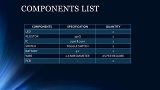
NAGPUR INSTITUTE OF TECHNOLOGY
FACULTY :-
PROF. BHAGESHREE WANKHEDE
NIT POLYTECHNIC
MICRO PROJECT OF DIGITALTECHNIQUE
Presented By :-
Ashish Sadavarti
DIGITAL IC TESTER
USING UNIVERSAL
GATES
CONTENTS
 COURSE OUTCOMES
 INTRODUCUTION
 COMPONENT LIST
 CIRCUIT DIAGRAM
 WORKING OF CIRCUIT
 ADVANTAGES & DISADVANTAGES
 APPLICATION
 OUTPUT
COURSE OUTCOMES
 Understand the concept of DIGITAL IC TESTER
FOR UNIVERSAL GATES
 Understand the working of DIGITAL IC TESTER.
 Use boolean expression to realize logic gates
 Build simple combinational circuit
INTRODUCTION
• It is a Digital ICTester. An Integrated Circuit tester (IC tester) is
used to test Integrated Circuits (ICs). This IC tester can be used
to test a wide variety of IC’s which includes simple logic gates and
also sequential and combinational ICs like flip-flops, counters, shift
registers etc. It is portable and easy to use.
•
COMPONENTS LIST
COMPONENTS SPECIFICATION QUANTITY
LED 2
RESISTOR 330Ω 2
IC 7400 & 7402 2
SWITCH TOGGLE SWITCH 2
BATTARY 9 V 1
WIRE 0.6 MM DIAMETER AS PER REQUIRE
PCB - 1
CIRCUIT DIAGRAM
 It is a integrated circuit tester (IC
tester) is used to test integrated circuits
(IC’s).
 We can easily test any digital IC using
this kind of an IC tester.
 This IC tester is constructed using
UNIVERSALGATES(NAND & NOR) with
a switch and a LED unit.
 It can test digital IC’s having a ON/OFF
WORKING
 NAND GATE
A LOW (0) OUTPUT RESULTS ONLY IF ALL THE INPUTS TO
THE GATE ARE HIGH (1); IF ANY INPUT IS LOW (0), A HIGH (1)
OUTPUT RESULTS. A NAND GATE IS MADE USING TRANSISTORS
AND JUNCTION DIODES. THE NAND GATE IS SIGNIFICANT
BECAUSE ANY BOOLEAN FUNCTION CAN BE IMPLEMENTED BY
USING A COMBINATION OF NAND GATES.
 NOR GATE
THE NOR GATE IS A DIGITAL LOGIC GATE THAT IMPLEMENTS
LOGICAL NOR. A HIGH OUTPUT (1) RESULTS IF BOTH THE INPUTS
TO THE GATE ARE LOW (0), IF ONE OR BOTH INPUT IS HIGH (1), A
LOW OUTPUT (0) RESULTS. NOR IS THE RESULT OF THE NEGATION
OF THE OR OPERATOR.
ADVANTAGE
It will give the same
outcome, however,
the NOR gate gives
the advantage that it needs
little space, less material
and is less complicated. At
least one input must be
active to stop the output
power.
• Cost: NAND is cost-effective
per byte and has a high storage
capacity for its physical size. -
Endurance: NAND cells
eventually wear out as their
transistors degrade.
A NAND chip lasts until it
reaches its write-cycle limit,
after which it will no longer be
able to store new data
APPLICATION
 In arithmetic logic unit of processors
 Increment and decrement operators
 Calculate addresses
 Use in multiplexers
 Computer memory & registers
 Microprocessor
Skill Develop
• Basic circuit knowledge :- electronic circuit desire can become can become a very
complex topic especially where large installation are concerned. Become of this
basic circuit knowledge is very important
• Design pcb:-
 Basic understanding of pcb.
 Knowledge of fundamentals in basic electronic to design pcb for circuit like
digital ic tester circuit. etc.
 we understand that how to done etchingon plane pcb carefully and perfectly.
 Improved technical ideas and knowledge related fm radio circuit.
 Now I can able to do sholdering of components on pcb after this work is done.
 Develop mounting the components on pcb with correct terminal of them.
OUTPUT
DIGITAL IC TESTER USING UNIVERSAL GATES.pptx

DIGITAL IC TESTER USING UNIVERSAL GATES.pptx

  • 1.
    NAGPUR INSTITUTE OFTECHNOLOGY FACULTY :- PROF. BHAGESHREE WANKHEDE NIT POLYTECHNIC MICRO PROJECT OF DIGITALTECHNIQUE Presented By :- Ashish Sadavarti
  • 2.
    DIGITAL IC TESTER USINGUNIVERSAL GATES
  • 3.
    CONTENTS  COURSE OUTCOMES INTRODUCUTION  COMPONENT LIST  CIRCUIT DIAGRAM  WORKING OF CIRCUIT  ADVANTAGES & DISADVANTAGES  APPLICATION  OUTPUT
  • 4.
    COURSE OUTCOMES  Understandthe concept of DIGITAL IC TESTER FOR UNIVERSAL GATES  Understand the working of DIGITAL IC TESTER.  Use boolean expression to realize logic gates  Build simple combinational circuit
  • 5.
    INTRODUCTION • It isa Digital ICTester. An Integrated Circuit tester (IC tester) is used to test Integrated Circuits (ICs). This IC tester can be used to test a wide variety of IC’s which includes simple logic gates and also sequential and combinational ICs like flip-flops, counters, shift registers etc. It is portable and easy to use. •
  • 6.
    COMPONENTS LIST COMPONENTS SPECIFICATIONQUANTITY LED 2 RESISTOR 330Ω 2 IC 7400 & 7402 2 SWITCH TOGGLE SWITCH 2 BATTARY 9 V 1 WIRE 0.6 MM DIAMETER AS PER REQUIRE PCB - 1
  • 7.
    CIRCUIT DIAGRAM  Itis a integrated circuit tester (IC tester) is used to test integrated circuits (IC’s).  We can easily test any digital IC using this kind of an IC tester.  This IC tester is constructed using UNIVERSALGATES(NAND & NOR) with a switch and a LED unit.  It can test digital IC’s having a ON/OFF
  • 8.
    WORKING  NAND GATE ALOW (0) OUTPUT RESULTS ONLY IF ALL THE INPUTS TO THE GATE ARE HIGH (1); IF ANY INPUT IS LOW (0), A HIGH (1) OUTPUT RESULTS. A NAND GATE IS MADE USING TRANSISTORS AND JUNCTION DIODES. THE NAND GATE IS SIGNIFICANT BECAUSE ANY BOOLEAN FUNCTION CAN BE IMPLEMENTED BY USING A COMBINATION OF NAND GATES.  NOR GATE THE NOR GATE IS A DIGITAL LOGIC GATE THAT IMPLEMENTS LOGICAL NOR. A HIGH OUTPUT (1) RESULTS IF BOTH THE INPUTS TO THE GATE ARE LOW (0), IF ONE OR BOTH INPUT IS HIGH (1), A LOW OUTPUT (0) RESULTS. NOR IS THE RESULT OF THE NEGATION OF THE OR OPERATOR.
  • 9.
    ADVANTAGE It will givethe same outcome, however, the NOR gate gives the advantage that it needs little space, less material and is less complicated. At least one input must be active to stop the output power. • Cost: NAND is cost-effective per byte and has a high storage capacity for its physical size. - Endurance: NAND cells eventually wear out as their transistors degrade. A NAND chip lasts until it reaches its write-cycle limit, after which it will no longer be able to store new data
  • 10.
    APPLICATION  In arithmeticlogic unit of processors  Increment and decrement operators  Calculate addresses  Use in multiplexers  Computer memory & registers  Microprocessor
  • 11.
    Skill Develop • Basiccircuit knowledge :- electronic circuit desire can become can become a very complex topic especially where large installation are concerned. Become of this basic circuit knowledge is very important • Design pcb:-  Basic understanding of pcb.  Knowledge of fundamentals in basic electronic to design pcb for circuit like digital ic tester circuit. etc.  we understand that how to done etchingon plane pcb carefully and perfectly.  Improved technical ideas and knowledge related fm radio circuit.  Now I can able to do sholdering of components on pcb after this work is done.  Develop mounting the components on pcb with correct terminal of them.
  • 12.