This document contains 52 questions and answers related to digital electronics and concepts such as digital gates, universal gates, truth tables, D'Morgan's theorem, adders, subtractors, comparators, flip-flops, counters, and integrated circuits. The questions would be suitable for a digital electronics viva or interview.
![ENGINEERING FUNDA YOUTUBE CHANNEL PROF. HITESH DHOLAKIYA
DIGITAL ELECTRONICS VIVA AND INTERVIEW QUESTIONS
ENGINEERING FUNDA YOUTUBE CHANNEL
Ans Magnitude Comparator. This Magnitude Comparator can be used perform comparisons
of two 8-bit binary or BCD words. The output provides both a P equals Q function or P
greater than Q function. A Magnitude Comparator would be considered standard logic
or glue logic when a discrete IC is used. However, because of the internal complexity, a
Magnitude Comparator would also be considered an MSI Function [Medium Scale
Integration].
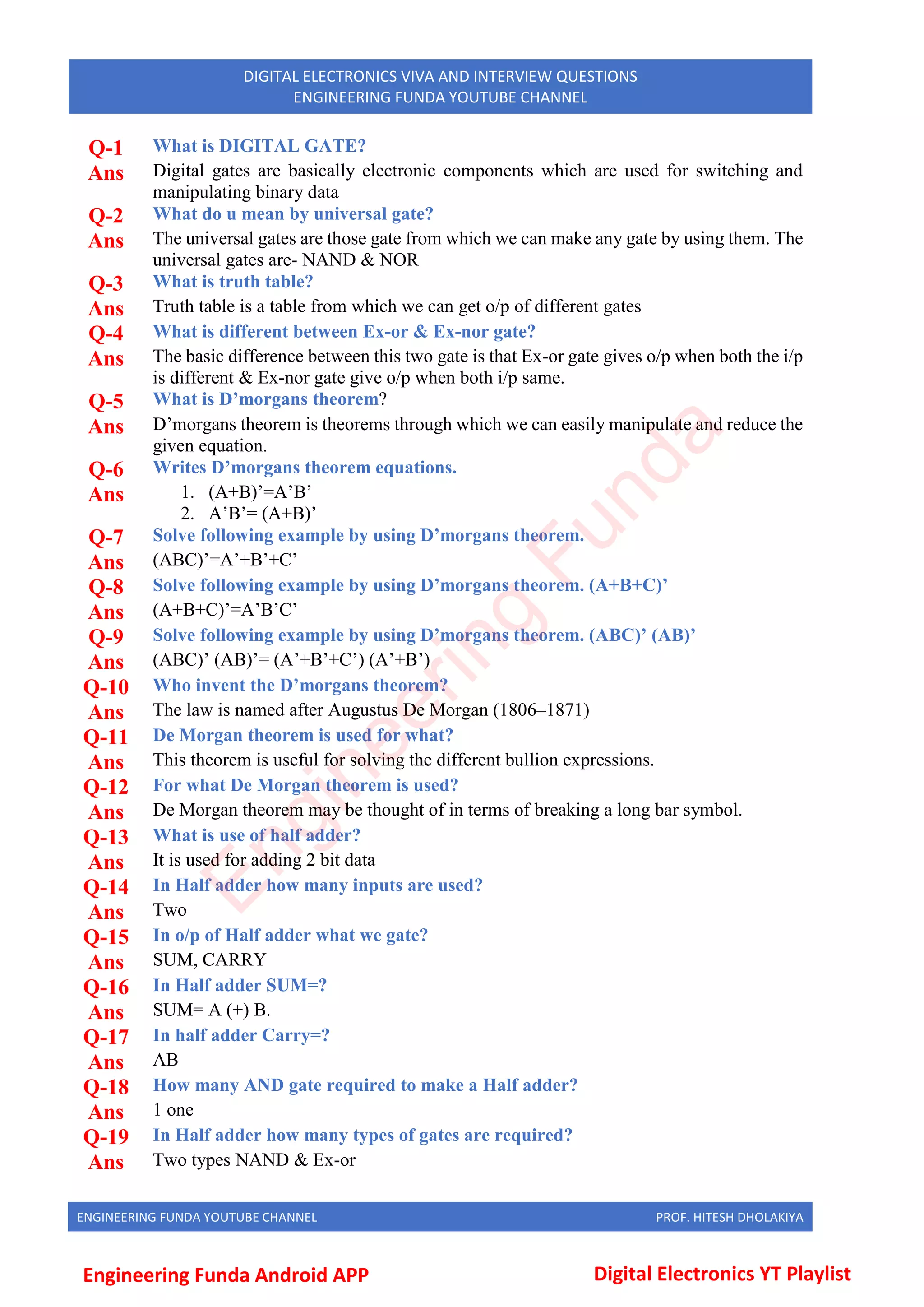
Q-53 What is IC?
Ans In electronics, an integrated circuit (also known as IC, chip, or microchip) is a
miniaturized electronic circuit (consisting mainly of semiconductor devices, as well as
passive components) that has been manufactured in the surface of a thin substrate of
semiconductor material. Integrated circuits are used in almost all electronic equipment
in use today and have revolutionized the world of electronics. Computers, cellular
phones, and other digital appliances are now inextricable parts of the structure of modern
societies, made possible by the low cost of production of integrated circuits.
Q-54 Tell about advancement in integrated circuits?
Ans Among the most advanced integrated circuits are the microprocessors or ’cores’, which
control everything from computers and cellular phones to digital microwave ovens.
Digital memory chips and ASICs are examples of other families of integrated circuits
that are important to the modern information society. While the cost of designing and
developing a complex integrated circuit is quite high, when spread across typically
millions of production units the individual IC cost is minimized. The performance of
ICs is high because the small size allows short traces which in turn allows low power
logic (such as CMOS) to be used at fast switching speeds.
Q-55 What is flip-flop?
Ans Flip-flop is a 1 bit storing element.
Q-56 How many types of flip-flop are used?
Ans 4 types of flip –flop, S-R, J-K, D, T
Q-57 What is disadvantage of SR flip-flop?
Ans When both the input is one then it gives invalid output.
Q-58 What is disadvantage of JK flip-flop?
Ans Race around condition.
Q-59 To remove race around condition what we use?
Ans Master slave Flip-flop.
Q-60 What is race around condition?
Ans When pulse width is more than signal width then for signal change of pulse width many
no of times signal changes its state that is called race around condition.
Q-61 What are the characteristic equation for T flip-flop?
Ans Q = TQ’+ QT’
Q-62 Which Gates are used in SR flip flops to a JK flip-flop?
Ans NAND Gates
Q-63 D flip-flop is used for?
Ans Providing delay.
Q-64 What is full form of T flip-flop?
Ans Toggle flip-flop
Q-65 What is counter?
E
n
g
i
n
e
e
r
i
n
g
F
u
n
d
a](https://image.slidesharecdn.com/digitalelectronicsvivaandinterviewquestions-min-220610063512-652d84cd/75/Digital-Electronics-viva-and-interview-questions-min-pdf-5-2048.jpg)
![ENGINEERING FUNDA YOUTUBE CHANNEL PROF. HITESH DHOLAKIYA
DIGITAL ELECTRONICS VIVA AND INTERVIEW QUESTIONS
ENGINEERING FUNDA YOUTUBE CHANNEL
Ans In digital logic and computing, a counter is a device which stores (and sometimes
displays) the number of times a particular event or process has occurred, often in
relationship to a clock signal.
Q-66 Give types of counter?
Ans There are two types of counters (1) Up counters, which increase (increment) in value (2)
Down counters, which decrease (decrement) in value.
Q-67 What are the implements of counter?
Ans In electronics, counters can be implemented quite easily using register-type circuits such
as the flip-flop, and a wide variety of designs exist, e.g.:
1. Asynchronous (ripple) counter – changing state bits are used as clocks to
subsequent state flip-flops
2. Synchronous counter – all state bits change under control of a single clock
3. Decade counter – counts through ten states per stage
4. Up–down counter – counts both up and down, under command of a control input
5. Ring counter – formed by a shift register with feedback connection in a ring
6. Johnson counter – a twisted ring counter
7. Cascaded counter
Q-68 Explain Asynchronous (ripple) counter?
Ans An asynchronous (ripple) counter is a single K-type flip-flop, with its J (data) input fed
from its own inverted output. This circuit can store one bit, and hence can count from
zero to one before it overflows (starts over from 0). This counter will increment once
for every clock cycle and takes two clock cycles to overflow, so every cycle it will
alternate between a transition from 0 to 1 and a transition from 1 to 0. Notice that this
creates a new clock with a 50percent duty cycle at exactly half the frequency of the input
clock. If this output is then used as the clock signal for a similarly arranged D flip-flop
(remembering to invert the output to the input), you will get another 1 bit counter that
counts half as fast. Putting them together yields a two bit counter.
Q-69 Explain Johnson counter?
Ans A Johnson counter (or switch tail ring counter, twisted-ring counter, walking-ring
counter, or Moebius counter) is a modified ring counter, where the output from the last
stage is inverted and fed back as input to the first stage.[2][3][4] A pattern of bits equal
in length to twice the length of the shift register thus circulates indefinitely. These
counters find specialist applications, including those similar to the decade counter,
digital to analog conversion, etc. it can be established by D flip flop and JK flip flop.
Q-70 Explain Decade counter?
Ans A decade counter is one that counts in decimal digits, rather than binary. A decade
counter may have each digit binary encoded (that is, it may count in binary-coded
decimal, as the 7490 integrated circuit did) or other binary encodings (such as the binary
encoding of the 7490 integrated circuit). Alternatively, it may have a fully decoded or
one-hot output code in which each output goes high in turn; the 4017 is such a circuit.
The latter type of circuit finds applications in multiplexers and demultiplexer, or
wherever a scanning type of behaviour is useful. Similar counters with different numbers
of outputs are also common.
Q-71 What is synchronous counters?
Ans In synchronous counters, the clock inputs of all the flip-flops are connected together and
are triggered by the input pulses. Thus, all the flip-flops change state simultaneously (in
parallel). The circuit below is a 3-bit synchronous counter. The J and K inputs of FF0
are connected to HIGH. FF1 has its J and K inputs connected to the output of FF0, and
E
n
g
i
n
e
e
r
i
n
g
F
u
n
d
a](https://image.slidesharecdn.com/digitalelectronicsvivaandinterviewquestions-min-220610063512-652d84cd/75/Digital-Electronics-viva-and-interview-questions-min-pdf-6-2048.jpg)