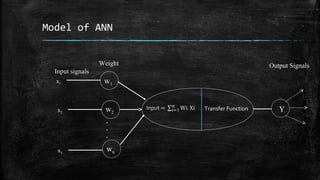
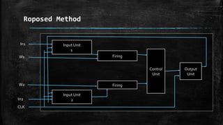
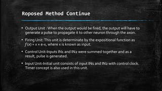
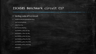
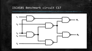
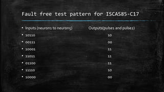
Design and Implementation of
Neural Network Based
circuits for VLSI testing
By K.P. Sridhar, B.Vignesh, S. Saravanan, M. Lavanya andV.Vaithiyanathan form School of
Computing, SASTRA University, India. In 2014,WorldApplied Sciences Journal 29 (Data Mining and
Soft ComputingTechniques).
Presented by
Name: Omar Faruq
ID:12131103065
Intake: 22nd
& Sec.:02
Email: mofs.shovo@gmail.com
Content
▪ Artificial Neural Network
▪ Model of ANN
▪ Transfer Function of ANN model
▪ Roposed Method
▪ ISCAS85 Combinational Benchmark circuit
▪ RESULTS AND DISCUSSION
▪ Conclusion
What is ANN?
▪ A neural network can be defined as a model of reasoning based on the
human brain.
▪ The brain consists of a densely interconnected set of nerve cells
(information processing units) called neurons.
▪ Human brain has 10 billion neurons and 60 trillion connections.
▪ Application of ANN
▪ Robotics
▪ Traveling Saleman's Problem
▪ Data processing, including filtering, clustering.
Analogy
Inputs represent synapses
Weights represent the strengths of synaptic links
Wire presents dendrite secretion
Summation block represents the addition of the secretions
Output represents axon voltage
Model of ANN
w1
w2
wn
Y
.
.
.
x1
x2
x3
Input signals
Weight Output Signals
Transfer Function
Transfer Function of ANN model
▪ Three transfer function in ANN
▪ Step Function
▪ Ramp Function
▪ Sigmoid Function
Backpropagation algorithm
is the squared error,
Sigmoid function & differentiable
Modell Of ANN
▪ Neuron will activated then when it has output logic is ‘1’ and in other
remaining cases it tends to ‘0’.
▪ Dendrite of neuron is considered as fan-in for node.
▪ axon is considered as fan-out.
▪ Node will burst firing patterns and reproduces spiking pulses in ANN
based combinational circuit.
▪ Proposed neuron method is targeted to ISCAS85-C17 benchmark
circuit.
Model Of ANN
▪ Fan-Out: Different neuron sharing one
source neuron which means that a net
propagates a signal from one source
to “n” destinations.
▪ Fan-In:The Number of input to the
gate.
N
M
Roposed Method
Input Unit
1
Input Unit
2
Firing
Firing
Control
Unit
Output
Unit
In1
W1
W2
In2
CLK
Roposed Method Continue
▪ Proposed design is divided into four major units such as
– Input unit
– Firing Unit
– Control Unit
– Output Unit
▪ There are IN1 & IN2 is referred as input andW1 &W2 referred to as
dendrites from others neurons along with relation weight and finally
a clock signal.
▪ Output Unit :When the output would be fired, the output will have to
generate a pulse to propagate it to other neuron through the axon.
▪ Firing Unit:This unit is determinate by the expositional function as
f (x) = x × e-x, where x is known as input.
▪ Control Unit-Inputs IN1 and IN2 were summed together and as a
result, pulse is generated.
▪ Input Unit-Initial unit consists of input IN1 and IN2 with control clock.
Timer concept is also used in this unit.
Roposed Method Continue
Benchmark circuit
▪ Some Benchmark circuits are:-
▪ ISCA is short form of “International Symposium on Circuits and
Systems”.
– ISCAS '85
▪ List: c1, c5, c17, c432, c499, c880, c1355, c1908, c2670, c3540, c5315, c6288, c7552
– ISCAS '89
– 74X-series
ISCAS85 Benchmark circuit C17
▪ Verilog code of C17 circuit
▪ module c17 (N1,N2,N3,N6,N7,N22,N23);
▪ input N1,N2,N3,N6,N7;
▪ output N22,N23;
▪ wire N10,N11,N16,N19;
▪ nand NAND2_1 (N10, N1, N3);
▪ nand NAND2_2 (N11, N3, N6);
▪ nand NAND2_3 (N16, N2, N11);
▪ nand NAND2_4 (N19, N11, N7);
▪ nand NAND2_5 (N22, N10, N16);
▪ nand NAND2_6 (N23, N16, N19);
▪ endmodule
ISCAS85 Benchmark circuit C17
Graphical representation of ISCAS85-C17
neuron
RESULTS AND DISCUSSION
▪ Proposed hardware based neuron design is implemented withVHDL
code.
▪ Proposed design is implemented to XILINX Spartan III FPGA
▪ Simulation of ISCAS85-C17 neuron Architecture usingVHDL code.
Fault free test pattern for ISCAS85-C17
▪ Inputs (neuron1 to neuron5) Outputs(pulse1 and pulse2)
▪ 10110 10
▪ 00111 00
▪ 10001 11
▪ 11011 11
▪ 01100 11
▪ 11110 10
▪ 10000 00
CONCLUSION
▪ The aim of the proposed method is to have the possibility of
interconnect more number of artificial neurons to create a complete
neuronal network inVLSI design testing.
Thank You
Do you have any question ?

Design and implementation of neural network based circuits for vlsi testing

  • 1.
    Design and Implementationof Neural Network Based circuits for VLSI testing By K.P. Sridhar, B.Vignesh, S. Saravanan, M. Lavanya andV.Vaithiyanathan form School of Computing, SASTRA University, India. In 2014,WorldApplied Sciences Journal 29 (Data Mining and Soft ComputingTechniques). Presented by Name: Omar Faruq ID:12131103065 Intake: 22nd & Sec.:02 Email: mofs.shovo@gmail.com
  • 2.
    Content ▪ Artificial NeuralNetwork ▪ Model of ANN ▪ Transfer Function of ANN model ▪ Roposed Method ▪ ISCAS85 Combinational Benchmark circuit ▪ RESULTS AND DISCUSSION ▪ Conclusion
  • 3.
    What is ANN? ▪A neural network can be defined as a model of reasoning based on the human brain. ▪ The brain consists of a densely interconnected set of nerve cells (information processing units) called neurons. ▪ Human brain has 10 billion neurons and 60 trillion connections. ▪ Application of ANN ▪ Robotics ▪ Traveling Saleman's Problem ▪ Data processing, including filtering, clustering.
  • 4.
    Analogy Inputs represent synapses Weightsrepresent the strengths of synaptic links Wire presents dendrite secretion Summation block represents the addition of the secretions Output represents axon voltage
  • 5.
    Model of ANN w1 w2 wn Y . . . x1 x2 x3 Inputsignals Weight Output Signals Transfer Function
  • 6.
    Transfer Function ofANN model ▪ Three transfer function in ANN ▪ Step Function ▪ Ramp Function ▪ Sigmoid Function
  • 7.
    Backpropagation algorithm is thesquared error, is the squared error, is the squared error,
  • 8.
    Sigmoid function &differentiable
  • 9.
    Modell Of ANN ▪Neuron will activated then when it has output logic is ‘1’ and in other remaining cases it tends to ‘0’. ▪ Dendrite of neuron is considered as fan-in for node. ▪ axon is considered as fan-out. ▪ Node will burst firing patterns and reproduces spiking pulses in ANN based combinational circuit. ▪ Proposed neuron method is targeted to ISCAS85-C17 benchmark circuit.
  • 10.
    Model Of ANN ▪Fan-Out: Different neuron sharing one source neuron which means that a net propagates a signal from one source to “n” destinations. ▪ Fan-In:The Number of input to the gate. N M
  • 11.
    Roposed Method Input Unit 1 InputUnit 2 Firing Firing Control Unit Output Unit In1 W1 W2 In2 CLK
  • 12.
    Roposed Method Continue ▪Proposed design is divided into four major units such as – Input unit – Firing Unit – Control Unit – Output Unit ▪ There are IN1 & IN2 is referred as input andW1 &W2 referred to as dendrites from others neurons along with relation weight and finally a clock signal.
  • 13.
    ▪ Output Unit:When the output would be fired, the output will have to generate a pulse to propagate it to other neuron through the axon. ▪ Firing Unit:This unit is determinate by the expositional function as f (x) = x × e-x, where x is known as input. ▪ Control Unit-Inputs IN1 and IN2 were summed together and as a result, pulse is generated. ▪ Input Unit-Initial unit consists of input IN1 and IN2 with control clock. Timer concept is also used in this unit. Roposed Method Continue
  • 14.
    Benchmark circuit ▪ SomeBenchmark circuits are:- ▪ ISCA is short form of “International Symposium on Circuits and Systems”. – ISCAS '85 ▪ List: c1, c5, c17, c432, c499, c880, c1355, c1908, c2670, c3540, c5315, c6288, c7552 – ISCAS '89 – 74X-series
  • 15.
    ISCAS85 Benchmark circuitC17 ▪ Verilog code of C17 circuit ▪ module c17 (N1,N2,N3,N6,N7,N22,N23); ▪ input N1,N2,N3,N6,N7; ▪ output N22,N23; ▪ wire N10,N11,N16,N19; ▪ nand NAND2_1 (N10, N1, N3); ▪ nand NAND2_2 (N11, N3, N6); ▪ nand NAND2_3 (N16, N2, N11); ▪ nand NAND2_4 (N19, N11, N7); ▪ nand NAND2_5 (N22, N10, N16); ▪ nand NAND2_6 (N23, N16, N19); ▪ endmodule
  • 16.
  • 17.
    Graphical representation ofISCAS85-C17 neuron
  • 18.
    RESULTS AND DISCUSSION ▪Proposed hardware based neuron design is implemented withVHDL code. ▪ Proposed design is implemented to XILINX Spartan III FPGA ▪ Simulation of ISCAS85-C17 neuron Architecture usingVHDL code.
  • 19.
    Fault free testpattern for ISCAS85-C17 ▪ Inputs (neuron1 to neuron5) Outputs(pulse1 and pulse2) ▪ 10110 10 ▪ 00111 00 ▪ 10001 11 ▪ 11011 11 ▪ 01100 11 ▪ 11110 10 ▪ 10000 00
  • 20.
    CONCLUSION ▪ The aimof the proposed method is to have the possibility of interconnect more number of artificial neurons to create a complete neuronal network inVLSI design testing.
  • 21.
    Thank You Do youhave any question ?