Implementation of Feed Forward Neural Network for Classification by Educational Board using Software Hardware Interfacing

in the last few years, the electronic devices production field has witness a great revolution by having the new birth of the extraordinary FPGA (Field Programmable Gate Array) family platforms. These platforms are the optimum and best choice for the modern digital systems now a day. The parallel structure of a neural network makes it potentially fast for the computation of certain tasks. The same feature makes a neural network well suited for implementation in VLSI technology. In this paper a hardware design of an artificial neural network on Field Programmable Gate Arrays (FPGA) is presented. Digital system architecture is designed to realize a feed forward multilayer neural network. The designed architecture is described using Very High Speed Integrated Circuits Hardware Description Language (VHDL).General Terms-Network.

Recommended
Recommended
More Related Content
What's hot
What's hot (20)
Similar to Implementation of Feed Forward Neural Network for Classification by Educational Board using Software Hardware Interfacing
Similar to Implementation of Feed Forward Neural Network for Classification by Educational Board using Software Hardware Interfacing (20)
More from ijsrd.com
More from ijsrd.com (20)
Recently uploaded
Recently uploaded (20)
Implementation of Feed Forward Neural Network for Classification by Educational Board using Software Hardware Interfacing
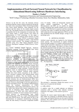
- 1. IJSRD - International Journal for Scientific Research & Development| Vol. 1, Issue 9, 2013 | ISSN (online): 2321-0613 All rights reserved by www.ijsrd.com 1913 Implementation of Feed Forward Neural Network for Classification by Educational Board using Software Hardware Interfacing Monika A. Wadhai 1 1 Department of Electronics and Telecommunication Engineering 1 RAIT College of Technology (Mumbai University), Nerul, Navi Mumbai, Maharashtra, India Abstract—in the last few years, the electronic devices production field has witness a great revolution by having the new birth of the extraordinary FPGA (Field Programmable Gate Array) family platforms. These platforms are the optimum and best choice for the modern digital systems now a day. The parallel structure of a neural network makes it potentially fast for the computation of certain tasks. The same feature makes a neural network well suited for implementation in VLSI technology. In this paper a hardware design of an artificial neural network on Field Programmable Gate Arrays (FPGA) is presented. Digital system architecture is designed to realize a feed forward multilayer neural network. The designed architecture is described using Very High Speed Integrated Circuits Hardware Description Language (VHDL).General Terms- Network Key words: Artificial Neural Network, Hardware Description Language, Field Programmable Gate Arrays (FPGAs), Sigmoid Activation Function. I. INTRODUCTION Artificial neural networks (ANN) have found widespread deployment in a broad spectrum of classification, perception, association and control applications. The aspiration to build intelligent systems complemented with the advances in high speed computing has proved through simulation the capability of Artificial Neural Networks (ANN) to map, model and classify nonlinear systems. Real time applications are possible only if low cost high-speed neural computation is made realizable. Towards this goal numerous works on implementation of Neural Networks (NN) have been proposed .Artificial neural networks (ANNs) have been mostly concentrate on the ANNs is slower execution compared with hardware-based ANNs implemented in software. This has benefits, since the designer does not need to know the inner workings of neural network elements, but can Hardware-based ANNs have been implemented both Analogue application of the neural network. However, disadvantage in real-time applications of software and digital circuits. The analogue implementations exploit the nonlinear characteristics of CMOS (complementary metal-oxide Semiconductor) devices, but they suffer from thermal drift, inexact computation results and lack of reprogram ability. Digital hardware-based implementations of ANNs have been relatively scarce, reprehensive examples of recent research can be found in. Recent advances in reprogrammable logic enable implementing large ANNs on a single field-programmable gate array (FPGA) device. The main reason for this is the miniaturization of component manufacturing technology, where the data density of electronic components doubles every 18 months. ANNs are biologically inspired and require parallel computations in their nature. Microprocessors and DSPs are not suitable for parallel designs. Designing fully parallel modules can be available by ASICs and VLSIs but it is expensive and time consuming to develop such chips. In addition the design results in an ANN suited only for one target application. FPGAs not only offer parallelism but also flexible designs, savings in cost and design cycle. II. ARTIFICIAL NEURON Artificial neural networks are inspired by the biological neural systems. The transmission of signals biological neurons through synapses is a complex chemical process in which specific transmitter substances are released from the sending side of the synapse. The effect is to raise or lower the electrical potential inside the body of the receiving cell. If this potential reaches a threshold, the neuron fires. It is this characteristic of the biological neurons that the artificial neuron model proposed by McCulloch Pitts attempts to reproduce. Following neuron model shown figure (1) is widely used in artificial neural networks with some variations. The artificial neuron given in this figure has N inputs, denoted as P1, P2…..PR. Each line connecting these inputs to the neuron is assigned a weight, denoted as W1, W2…..WR respectively. Fig. 1: Structural diagram of a neuron The activation, a, determines whether the neuron is to be fired or not. It is given by the formula: ∑ (2.1) A negative value for a weight indicates an inhibitory connection while a positive value indicates excitatory connection. The output, y of the neuron is given as: y=f (a) (2.2) Originally the neuron output function f(a) in McCulloch Pitts model was proposed as threshold function, however linear, ramp, and sigmoid functions are also used in different situations. The vector notation can be used for expressing the activation of a neuron.
- 2. Implementation of Feed Forward Neural Network for Classification by Educational Board using Software Hardware Interfacing (IJSRD/Vol. 1/Issue 9/2013/0055) All rights reserved by www.ijsrd.com 1914 a=wT p (2.3) Here, the jth element of the input vector p is pj, the jth element of the weight vector of w is wj. Both of these vectors are of size R. A Neuro-computing system is made up of a number of artificial neurons and a huge number of interconnections between them. Figure (2) shows architecture of feed forward neural network. In layered neural networks, the neurons are organized in the form of layers. The neurons in a layer get inputs from the previous layer and feed their output to the next layer. These types of networks are called feed forward networks. Output connections from a neuron to the same or previous layer neuron are not permitted. The input layer is made of special input neurons, transmitting only the applied external input to their outputs. The last layer is called the output layer, and the layers other than input & output layers are called the hidden layers. In a network, if there are input and output layers only, then it is called a single layer network. Networks with one or more hidden layers are called multilayer networks. (Multilayer perception is well-known feed forward layered network, on which the Back propagation learning algorithm is widely implemented). The structures, where connections to the neurons are to the same layer or to the previous layers are called recurrent networks. Fig. 2: Layered Feed forward Neural Network Hopfield and Boltzmann Machine are examples of widely used recurrent networks. III. OVERVIEW OF VHDL VHDL is a language meant for describing digital electronic systems. In its simplest form, the description of a component in VHDL consists of an interface specification and an architectural specification. The interface description begins with the ENTITY keyword and contains the input- output ports of the component. The name of the component comes after the ENTITY keyword and is followed by IS, which is also a VHDL keyword. The description of the internal implementation of an entity is called an architecture body of the entity. There may be a number of different architecture bodies of an interface to an entity corresponding to alternative implementations that perform the same function. The alternative implementations of the architecture body of the entity are termed as Behavioral Description or Structural Description. After describing a digital system in VHDL, simulation of the VHDL code has to be carried out for two reasons. First, we need to verify whether the VHDL code correctly implements the intended design. Second, we need to verify that the design meets its specifications. Some synthesis tools are capable of implementing the digital system described by the VHDL code using a PGA (Programmable gate array) or CPLD (Complex programmable logic devices). The PLDs are capable of implementing a sequential network but not a complete digital system. Programmable gate arrays and complex programmable logic devices are more flexible and more versatile and can be used to implement a complete digital system on a single chip. A typical PGA is an IC that contains an array of identical logic cells with programmable interconnections. The user can program the functions realized by each logic cell and the connections between the cells. Such PGAs are often called FPGAs since they are field programmable. IV. THE PROPOSED DESIGN The proposed design consists of neuron architecture design. Neuron ArchitectureA. The processing element of an ANN is the Neuron. A Neuron can be viewed as processing data in three steps; the weighting of its input values, the summation of them all and their filtering by sigmoid function. The summation can be calculated by a serial accumulation. For the weighted inputs to be calculated in parallel using conventional design techniques, a large number of multiplier units would be required. To avoid this, Multiplier/Accumulator architecture has been selected. It takes the input serially, multiplies them with the corresponding weight and accumulates their sum in a register. The processes are synchronized to clock signal. The number of clock cycles for a neuron to finish its work, equals to the number of connections from the previous layer. The accumulator has a load signal, so that the bias values are loaded to all neurons at start-up. Figure (3) shows the proposed neuron design. Fig. 3: Neuron Architecture Activation FunctionB. One of the most important parts of a neuron is its activation function. The nonlinearity of the activation function makes it possible to approximate any function. In the hardware implementation concept of neural networks, it is not so easy to realize sigmoid activation functions. Special attention must be paid to an area-efficient implementation of every computational element when implementing large ANNs on digital hardware. This holds true for the nonlinear activation function used at the output of neurons. A common activation function is the sigmoid function. Efficient implementation of the sigmoid function on an FPGA is a difficult challenge faced by designers. It is not suitable for direct implementation because it consists of an infinite exponential series. In most cases computationally simplified alternatives of sigmoid function are used.
- 3. Implementation of Feed Forward Neural Network for Classification by Educational Board using Software Hardware Interfacing (IJSRD/Vol. 1/Issue 9/2013/0055) All rights reserved by www.ijsrd.com 1915 Fig. 4: Transfer Function Block diagram of the DE-I Board:C. The block diagram of the DE1 board is shown in Figure 5. To provide maximum flexibility for the user all connections are made through the Cyclone II FPGA device. Thus, the user can configure the FPGA to implement any system design. Fig. 5: Block diagram of DE-I Board V. DISCUTION AND RESULT The purpose of the paper is to learn how to connect simple input and output to an FPGA chip and implement circuit using this Device. Fig. 6: Simulation Result of Hidden Layer Fig: 7 Simulation Result of Output Layer VI. CONCLUSION This paper presents design solution to eliminate the FPGA design for an Artificial Neural Network. The motivation for this study stems from the fact that an FPGA coprocessor with limited logic density and capabilities can used in building Artificial Neural Network which is widely used in solving different problems. Future work involves estimating the maximum size of ANNs in modern FPGAs. The main points are the size and parameter inability of multipliers and the number of interlayer interconnections. The first defines mainly the required area resources and the second defines the required routing. ACKNOWLEDGMENTS We thanks to our guide who have guided us towards development of this project. REFERENCES [1] Haitham Kareem Ali and Esraa Zeki Mohammed, “Design Artificial Neural Network Using FPGA”, IJCSNS International Journal of Computer Science and Network Security, VOL. 10 No.8, August 2010. [2] Saumil Merchant, Gregory D. Peterson, Sang Ki Park, and Seong G. Kong, "FPGA Implementation of Evolvable Block-based Neural Network," IEEE Congress on Evolutionary Computation, 0-7803-9487- 9/06, 2006. [3] M. Krips, T. Lammert, and Anton Kummert, “FPGA Implementation of a Neural Network for a Real-Time Hand Tracking System”, Proceedings of the first IEEE International Workshop on Electronic Design, Test and Applications, 2002. [4] Volnei A. Pedroni Circuit Design with VHDL, Prentice Hall, India. [5] Altera DE1 Package “DE1 Development and Education Board”. [6] Altera User Manual (2006) “DE1 Development and Education Board”