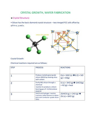
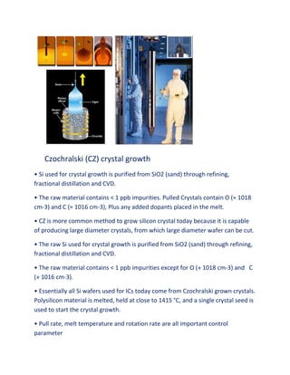
CRYSTAL GROWTH, WAFER FABRICATION
 Crystal

Structure:

• Silicon has the basic diamond crystal structure – two merged FCC cells offset by
a/4 in x, y and z.

Crystal Growth:
Chemical reactions required are as follows;
STEP

PROCESS

REACTIONS

1

Produce metallurgical grade
silicon (MGS) by heating silica
with carbon.

C(s) + SiO2 (s) Si (l) + SiO
(g) + CO(g)

2

Purify MG silicon through a
chemical
reaction to produce a siliconbearing gas of trichlorosilane
(SiHCl3)

Si (s) + 3HCl (g) SiHCl3(g)
+ H2 (g) + heat

3

SiHCl3 and hydrogen reaction
a process called Siemens to obtain
pure semi conductor- grade silicon
(SGS)

2SiHCl3 (g ) + 2H2 (g) 
2Si (s) + 6HCl (g)
Czochralski (CZ) crystal growth
• Si used for crystal growth is purified from SiO2 (sand) through refining,
fractional distillation and CVD.
• The raw material contains < 1 ppb impurities. Pulled Crystals contain O (≈ 1018
cm-3) and C (≈ 1016 cm-3), Plus any added dopants placed in the melt.
• CZ is more common method to grow silicon crystal today because it is capable
of producing large diameter crystals, from which large diameter wafer can be cut.
• The raw Si used for crystal growth is purified from SiO2 (sand) through refining,
fractional distillation and CVD.
• The raw material contains < 1 ppb impurities except for O (» 1018 cm-3) and C
(» 1016 cm-3).
• Essentially all Si wafers used for ICs today come from Czochralski grown crystals.
Polysilicon material is melted, held at close to 1415 °C, and a single crystal seed is
used to start the crystal growth.
• Pull rate, melt temperature and rotation rate are all important control
parameter
• Sequence of photographs and drawings illustrating
CZ crystal growth. The charge is melted,
• the seed is inserted, the neck region is grown at a high rate to remove
dislocations and finally the growth is
• slowed down to produce a uniform crystal.

THANK YOU………FOR GIVING ME SUCH OPPURTUNITY

PROFESSOR: MR SANJEEV BRAHMA
(VLSI TECHNOLOGY)

BY: KALYANI GAYAKWAD
ROLL NO: U11EC109
Wafer formation

Wafer formation

  • 1.
    CRYSTAL GROWTH, WAFERFABRICATION  Crystal Structure: • Silicon has the basic diamond crystal structure – two merged FCC cells offset by a/4 in x, y and z. Crystal Growth: Chemical reactions required are as follows; STEP PROCESS REACTIONS 1 Produce metallurgical grade silicon (MGS) by heating silica with carbon. C(s) + SiO2 (s) Si (l) + SiO (g) + CO(g) 2 Purify MG silicon through a chemical reaction to produce a siliconbearing gas of trichlorosilane (SiHCl3) Si (s) + 3HCl (g) SiHCl3(g) + H2 (g) + heat 3 SiHCl3 and hydrogen reaction a process called Siemens to obtain pure semi conductor- grade silicon (SGS) 2SiHCl3 (g ) + 2H2 (g)  2Si (s) + 6HCl (g)
  • 2.
    Czochralski (CZ) crystalgrowth • Si used for crystal growth is purified from SiO2 (sand) through refining, fractional distillation and CVD. • The raw material contains < 1 ppb impurities. Pulled Crystals contain O (≈ 1018 cm-3) and C (≈ 1016 cm-3), Plus any added dopants placed in the melt. • CZ is more common method to grow silicon crystal today because it is capable of producing large diameter crystals, from which large diameter wafer can be cut. • The raw Si used for crystal growth is purified from SiO2 (sand) through refining, fractional distillation and CVD. • The raw material contains < 1 ppb impurities except for O (» 1018 cm-3) and C (» 1016 cm-3). • Essentially all Si wafers used for ICs today come from Czochralski grown crystals. Polysilicon material is melted, held at close to 1415 °C, and a single crystal seed is used to start the crystal growth. • Pull rate, melt temperature and rotation rate are all important control parameter
  • 3.
    • Sequence ofphotographs and drawings illustrating CZ crystal growth. The charge is melted, • the seed is inserted, the neck region is grown at a high rate to remove dislocations and finally the growth is • slowed down to produce a uniform crystal. THANK YOU………FOR GIVING ME SUCH OPPURTUNITY PROFESSOR: MR SANJEEV BRAHMA (VLSI TECHNOLOGY) BY: KALYANI GAYAKWAD ROLL NO: U11EC109