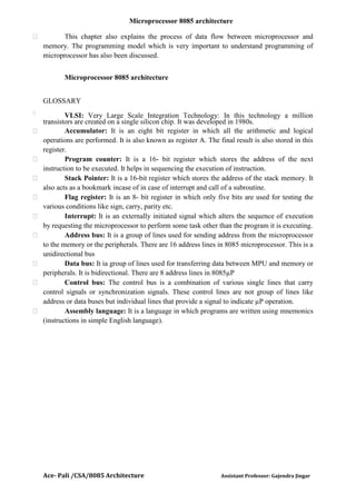
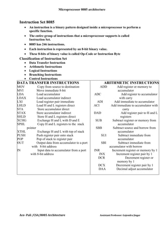
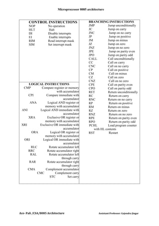
Microprocessor 8085 architecture
Ace- Pali /CSA/8085 Architecture Assistant Professor: Gajendra Jingar
UNIT - 4
Table of Contents
Chapter 4: Microprocessor 8085 architecture
3.1 Introduction
3.2 Block diagram of 8085
3.3 8085 system bus
3.4 8085 Pin description
3.5 Microprocessor operations
Microprocessor 8085 architecture
Ace- Pali /CSA/8085 Architecture Assistant Professor: Gajendra Jingar
3.1 Introduction
Intel 8085 is the most popular 8-bit microprocessor. It is a 40-pin IC fabricated on a
single VLSI chip. It requires a single +5V power supply. It has in-built clock generation,
system control and interrupt circuitry. The 8085 µP is a programmable digital device which
has got a set of instructions designed internally to manipulate the data and communicate with
peripherals. The internal logic organization or design is called architecture of the µP. It is
important to know the architecture because it is the internal architecture of a µP which
determines as to what happens to the data inside the µP and how and what type of operations
can be performed with the data.
3.2 Block diagram of 8085
To understand the architecture of 8085 µP it is necessary to discuss the block
diagram. Fig. 3.1 below shows the block diagram of 8085 µP. It mainly consists of three
sections
(a) Register unit
(b) Arithmetic and logic unit
(c) Timing and control unit
These important sections will be discussed in detail in the subsequent sections.
Register unit
The micro processor 8085 consists of different types of registers
(a) Accumulator
(b) General purpose register
(c) Flag register
(d) Temporary register
(e) Program counter
(f) Stack pointer
Accumulator:
It is an 8-bit register which is used for performing all the arithmetic’s and logical
operations. Accumulator is also known as ‘register A’. During any mathematical or logical
operation one of the operands should be present in the accumulator. The final result is also
stored in the accumulator.
Microprocessor 8085 architecture
Ace- Pali /CSA/8085 Architecture Assistant Professor: Gajendra Jingar
Fig. 3.1 Functional Block diagram
Microprocessor 8085 architecture
Ace- Pali /CSA/8085 Architecture Assistant Professor: Gajendra Jingar
General purpose registers:
There are six 8-bit general purpose registers B, C, D, E, H & L. General purpose
registers are used for temporary storage of data and intermediate results while the processor is
executing the program. Two eight bit registers can be combined for handling 16-bit data.
Combination of two 8-bit registers is known as pair. Valid register pairs are B-C, D-E, H-L.
The H-L pair is used to address memories.
Flag register:
It is an 8-bit register in which five flip flops are used for checking condition. These
flip flops are called flags. Each of these flags can have the value either one or zero to indicate
certain condition after arithmetic and and logical operation. The five flags present in 8085 µP
are:
(a) Sign flag (b) Zero flag (c) Auxiliary carry flag (d) Parity flag (e) Carry flag
Sign flag (S): After the execution of an arithmetic or logical operation, if bit D7 of the result is
1, the sign flag is set. This flag is used with signed numbers and has no relevance for
unsigned numbers. In a given byte, if D7 is 1, the number is said to be negative and if it is 0,
the number is considered as positive.
Zero Flag (Z): This flag is set if the result after arithmetic or logical operation turns out to be
zero and is reset if the result is non-zero.
Auxiliary carry (AC): This flag is set if in an arithmetic operation a carry is generated at bit
D3 and passed onto D4. This flag is used internally for BCD operations and is not available to
the user unlike other flags.
Parity (P): After an arithmetic or logical operation, if the result has an even number of 1s, the
flag is set and if there is odd number of 1s the flag is reset.
Carry (CY): If an arithmetic operation results in a carry, the flag is set otherwise it is reset. It
also serves as a borrow flag for subtraction.
The bit position reserved for these flags in the flag register are as follows:
S Z AC P CY
D0 D1 D2 D3 D4 D5 D6 D7
Temporary register:-
Register W and Z are known as temporary registers. They are used by the µP
for storing the data temporarily during execution of a program. They are 8-bit registers and
are not accessible to the user.
Microprocessor 8085 architecture
Ace- Pali /CSA/8085 Architecture Assistant Professor: Gajendra Jingar
Program Counter:
It is a 16-bit register which holds the address of the instructions. Initially it
indicates towards the starting address of the program but after the first instruction is fetched
the program counter automatically gets incremented by one and points towards the next
instruction. This process continues till the end of the program.
Stack pointer:
The stack pointer is a 16-bit register which basically serves two purposes
(a) Points towards the stack memory. Initially it indicates the beginning of the stack
memory. Whenever something is added to the stack, the stack pointer is decremented and
whenever something is removed from the stack the stack pointer is incremented. Hence the
stack pointer always points to the top of the stack.
(b) Stack pointer also points towards the memory location where the µP has to go after
attending an interrupt or a subroutine; therefore it acts as a bookmark.
Arithmetic and logic unit:
This is the unit where all the arithmetic operations like addition, subtraction,
multiplication and division and logical operations like AND, OR, Ex-OR, complement,
compare etc. are performed. It includes the accumulator, the temporary register, the
arithmetic and logic circuits and five flags. The temporary registers are used to store data
temporarily during an arithmetic/logical operation. The result is stored in the accumulator and
the flags are set or reset according to the result of the operation.
Timing and control unit:
The timing and control unit generates timing and control signals which are
necessary for the execution of instruction. It controls data flow between CPU and peripherals.
It provides status, control and timing signals which are required for the operation of memory
and I/O devices.
3.3 8085 System Bus
System bus is basically a group of communication lines/wires that are
responsible for transferring information between different units of the device or peripherals.
A typical microprocessor communicates with memory and other devices using three buses:
address bus, data bus and control bus.
Address bus: Address bus is a unidirectional group of 16 lines i.e. bits flow in one direction
from the µP to the peripheral devices. The 8085 µP with it’s 16 address lines is capable of
addressing 216
=65536 (64K) memory locations.
Data bus: Data bus carries data in binary form, between microprocessor and peripheral
devices as well as memory. It is a group of 8-bits and is bidirectional. Data bus also carries
instructions from memory to the microprocessor. Size of the bus therefore limits the number
of possible instructions. The 8085 µP has 246 bit patterns amounting to 74 different
instructions. These 74 different instructions are therefore called its instruction set.
6
Microprocessor 8085 architecture
Ace- Pali /CSA/8085 Architecture Assistant Professor: Gajendra Jingar
Control bus: The control bus is combination of various single lines that carry control signals.
The control lines are not group of lines like address and data bus but are individual lines.
Microprocessor generates specific control signals for every operation it performs.
The bus system of 8085 is shown in figure 3.2.
Figure 3.2 8085 Bus Structure
Value addition:
Evolution of microprocessor:
With the advances in L.S.I. (Large Scale Integration) and V.L.S.I. (Very Large
scale integration) technology it became possible to build the whole CPU of a digital computer
on a single IC (Integrated circuit). A CPU built on a single chip is called microprocessor.
The first microprocessor INTEL 4004 a 4-bit µP was introduced in 1971 by
INTEL corporation. In 1972 INTEL introduced the first 8-bit microprocessor 8080. These
microprocessors used PMOS technology. A more powerful and faster µP the INTEL 8080
using NMOS technology was introduced in 1973. A number of companies like Motorola,
Zilog, National Semiconductor etc. INTEL introduced 8-bit µP 8085 in 1976. It is very
popular and most widely used microprocessor. 8-bit microprocessors were soon followed by
16-bit microprocessors like INTEL 8086, 80186, 80286. Microprocessors like INTEL 80386,
80486 are 16-bit microprocessors that were introduced in 1980. The most powerful µP 80586
(PENTIUM) was introduced in 1989-1990. It is a 64-bit microprocessor. Since then there has
been a continuous development in this field of semiconductor technology.
Microprocessor 8085 architecture
Ace- Pali /CSA/8085 Architecture Assistant Professor: Gajendra Jingar
3.4 8085 Pin Description
Figure 3.2 Pin Configuration of 8085
The 8085 µP is an 8-bit microprocessor capable of addressing 64K of
memory. It is a 40-pin IC which requires a power supply of +5V and it’s operating frequency
is 3MHz. Fig. 3.3 shows the pin configuration of 8085 µP .The pin configuration of 8085 µP
can be classified into six groups namely:
 High order Address bus
 Multiplexed Address/Data bus
Microprocessor 8085 architecture
Ace- Pali /CSA/8085 Architecture Assistant Professor: Gajendra Jingar
 Control and status signals
 Power supply and frequency signals
 Externally initiated signals and
 Serial I/O ports
(1) High order address bus:
The address bus is a group of 16-lines generally identified as A0-A15. The
address bus is split into two segments ADO-AD7 and A 8-A15 .The buses from ADO-AD7 are
low order address buses and A8-A15 buses are high order address buses.
(2) Multiplexed Address/Data bus:
The data bus is a group of 8-lines used for transfer of data. These lines are
bidirectional i.e. data flows in both the directions from µP to peripherals and vice-versa. They
are represented as ADO-AD7 because they serve dual purpose. They are used as low-order
address bus as well as data bus and therefore they are known as multiplexed address/data bus.
(3) Control and status signals:
This group of signals includes two control signals, three status signals and one
special signal. These signals are as follows:
Control signal: - and ar the two control signals which indicate that the data is to be read from
or written into a selected memory or I/O location. Both are active low signals.
Status signal: - , S1 and SO are the three status signals. is used to differentiate between I/O
and memory operations. When it is high it indicates I/O operation and when it is low it
indicates memory operation. S1 and S O are also status signals but are rarely used in small
systems.
Special signal: - ALE (Address Latch Enable) is a special signal used for demultiplexing
address and data bus (ADO-AD7). It is a positive going pulse generated every time a machine
cycle begins and so long as it remains positive it indicates that the bits on ADO-AD7 are
address bits.
(4) Power supply and clock frequency:
The power supply required for 8085 µP is +5V. As shown in pinout diagram VCC is
connected to +5V and VSS is connected to the ground of the power supply. The µP operates
on frequency of 3MHz, therefore an oscillator of frequency 6MHz is connected between pin
no. 1 and 2 as the frequency is internally divided by two. CLK (OUT) i.e. Pin no. 37 is used
as a system clock for other devices.
(5) Externally initiated signals:
There are certain operations which can be initiated by external devices (or signals).
For these externally initiated operations there are individual pins assigned on the
Microprocessor 8085 architecture
Ace- Pali /CSA/8085 Architecture Assistant Professor: Gajendra Jingar
microprocessor chip. Interrupts are also considered as externally initiated signal. Here is a
brief explanation of interrupts and other externally initiated signals.
Interrupts: - The 8085 has five interrupt signals that can be used to interrupt a program
execution. These interrupts are
(a) TRAP: The interrupt with highest priority. It is non-maskable and vectored
interrupt i.e. the µP has to attend this interrupt immediately.
(b) RST 7.5, RST 6.5, RST 5.5: These are known as Restart interrupts and have
lower priority than TRAP but have higher priority than the INTR interrupt. They are vectored
and maskable interrupts. Among the three the priority order is RST7.5>RST6.5>RST5.5
(c) INTR: It is a general purpose interrupt. It is maskable and non-vectored
interrupt and has the least priority.
Reset: - When RESET pin is activated, the µP suspends all the internal operations and the
program counter is cleared. Now the program execution can again begin at the zero memory
address.
Ready: - The Ready signal is used to synchronize slower peripherals with the microprocessor.
If the signal at READY pin is low the microprocessor enters into a wait state.
Hold: - This signal is used by the external devices to request the microprocessor for using the
buses. When this signal is activated the µP leaves is control over the buses and makes them
free for the peripherals to use.
: - Interrupt Acknowledge. This signal is used to acknowledge an interrupt.
HLDA: - Hold Acknowledge. This signal is used to acknowledge the HOLD request.
: - This is an active low signal. When it is activated the buses are restated,
the program counter is cleared and the microprocessor is reset.
RESET OUT: This signal indicates that the microprocessor is being reset. It can be used to
reset other devices also.
(6) Serial I/O Ports:
To send and receive data serially microprocessor has two pins ‘SID’ and ‘SOD’ by using
these pins the µP can communicate with other µP and peripheral devices. In serial
transmission, data bits are sent over a single line, one bit at a time. SID is Serial Input Data
and SOD stands for Serial Output Data.
SID (Input) – On execution of the RIM instruction the data on this line is loaded into the
seventh bit of the accumulator.
SOD(output)- When SIM instruction is executed the 7th
bit of the accumulator is output on
SOD line.
3.5 Microprocessor operations
Microprocessor 8085 architecture
Ace- Pali /CSA/8085 Architecture Assistant Professor: Gajendra Jingar
The process of data manipulation and communication with peripherals is
determined by the logic design of the microprocessor. This logic design is called architecture.
All the operations of microprocessor can be classified into following types:
(a) Microprocessor initiated operations
(b) Internal operations
(c) Peripheral or externally initiated operations
Microprocessor initiated operations
Microprocessor initiated operations are usually one of the
following
operations :
(a) Memory read: Reads data from memory.
(b) Memory write: Writes data into the memory.
(c) I/O Read: Accepts data from input devices.
(d) I/O Write: Sends data to output devices
All these operations are initiated by microprocessor and executed by peripheral
devices as a part of communication process between microprocessor and memory or
peripheral devices. To perform these communication operations, the MPU needs to perform
following steps
(a) Identify the memory location or the peripheral devices.
(b) Provide synchronization signal i.e. timing signals.
(c) Transfer the binary information (data and instruction).
All these functions are performed with the help of communication lines called system
bus. The details of the three types of buses i.e. Address bus, data bus and control bus have
been discussed in section 3.1.2
Value addition:
Data flow between memory and MPU:
Figure below explains the flow of data between microprocessing unit and
memory. First of all the 16-bit address is placed on the address bus from the program counter.
In the figure it can be seen that the address is 2005H where the data is placed. The higher
order address i.e. 20H is placed on the address bus A8-A15 while the lower order address is
placed on the multiplexed address and data bus ADO-AD7. The lower order address continues
to remain on this address bus so long as ALE (Address Latch Enable) remains positive. Once
ALE goes low it carries data. The control unit sends the signal to indicate what type of
operation is to be performed. Since the data is to be read from the
memory therefore it sends to enable the memory chip. The byte from the memory location is
then placed on the data bus i.e. 4F saved in location 2005H is placed on the data bus and sent
to the instruction decoder. The instruction is decoded and accordingly the task is performed
by the ALU i.e. Arithmetic and logic unit.
Microprocessor 8085 architecture
Ace- Pali /CSA/8085 Architecture Assistant Professor: Gajendra Jingar
Internal data operations
These are the operations which are internally performed by the
microprocessor. They are classified into five groups:
1) Store 8-bit data
2) Perform arithmetic and logical operation
3) Test for the conditions
4) Sequence the execution of instructions
5) Store data temporarily during execution in the R/W memory locations called the
stack.
To perform these operations microprocessor requires registers, Arithmetic and logic
unit, buses and control unit.
To store 8-bit data microprocessor has six general purpose registers. During program
execution, these registers are used to store 8- or 16-bit data. The details of these registers i.e.
B, C, D, E, H and L have already been discussed in register unit.
Arithmetic and logical operations are performed in accumulator and the conditions
are tested by the flag register. Program counter is used to sequence the execution of
instructions and stack memory is used for temporary storage of data during execution and
stack pointer is used to address the stack memory.
Peripheral or Externally initiated operations
There are four externally initiated operations, for which individual pins on the
microprocessor chip are assigned. These operations are RESET, READY, HOLD and
INTERRUPT. The details of all these operations have been discussed in section 3.1.2
Value addition:
8085 Programming Model:
A programming model is a conceptual representation of a real object and can be
in the form of a text, a drawing or a built structure. Here is a programming model of 8085
which gives information required to write a program. It consists of some segments of ALU
and the registers. This model includes six general purpose registers, accumulator, flag
register, program counter and stack pointer. This model is not a reflection of physical
structure of the microprocessor but gives all the information that is relevant for writing an
assembly language program. Figure below shows the programming model specific to the
8085 microprocessor.
Microprocessor 8085 architecture
Ace- Pali /CSA/8085 Architecture Assistant Professor: Gajendra Jingar
Figure: 8085 Programming model
SUMMARY
This chapter describes the architecture of the 8085 microprocessor. The important concepts
which have been explained in this chapter are summarized below:
 Various functional units present in 8085 like register unit, arithmetic and logic unit
and timing and control unit have been explained with the help of block diagram.
 Register unit consists of six general purpose registers namely B, C, D, E, H and L,
two temporary registers W and Z, two 16-bit registers SP(stack pointer) and PC(program
counter).
 Accumulator is register A where all the mathematical and logical operations are
performed and final result is stored
 Besides pinout diagram the signals of microprocessor 8085 have been discussed. The
signals of 8085 µP can be classified into six groups: High order Address bus, Multiplexed
Address/Data bus, Control and status signals, Power supply and frequency signals, Externally
initiated signals and Serial I/O ports.
 The operations performed by microprocessor can be classified into three types (a)
Microprocessor initiated operations (b) Internal data operations (c) Externally initiated
operations.
Microprocessor 8085 architecture
Ace- Pali /CSA/8085 Architecture Assistant Professor: Gajendra Jingar
 This chapter also explains the process of data flow between microprocessor and
memory. The programming model which is very important to understand programming of
microprocessor has also been discussed.
Microprocessor 8085 architecture
GLOSSARY

VLSI: Very Large Scale Integration Technology: In this technology a million
transistors are created on a single silicon chip. It was developed in 1980s.
 Accumulator: It is an eight bit register in which all the arithmetic and logical
operations are performed. It is also known as register A. The final result is also stored in this
register.
 Program counter: It is a 16- bit register which stores the address of the next
instruction to be executed. It helps in sequencing the execution of instruction.
 Stack Pointer: It is a 16-bit register which stores the address of the stack memory. It
also acts as a bookmark incase of in case of interrupt and call of a subroutine.
 Flag register: It is an 8- bit register in which only five bits are used for testing the
various conditions like sign, carry, parity etc.
 Interrupt: It is an externally initiated signal which alters the sequence of execution
by requesting the microprocessor to perform some task other than the program it is executing.
 Address bus: It is a group of lines used for sending address from the microprocessor
to the memory or the peripherals. There are 16 address lines in 8085 microprocessor. This is a
unidirectional bus
 Data bus: It ia group of lines used for transferring data between MPU and memory or
peripherals. It is bidirectional. There are 8 address lines in 8085µP
 Control bus: The control bus is a combination of various single lines that carry
control signals or synchronization signals. These control lines are not group of lines like
address or data buses but individual lines that provide a signal to indicate µP operation.
 Assembly language: It is a language in which programs are written using mnemonics
(instructions in simple English language).
Microprocessor 8085 architecture
Ace- Pali /CSA/8085 Architecture Assistant Professor: Gajendra Jingar
Instruction Set 8085
 An instruction is a binary pattern designed inside a microprocessor to perform a
specific function.
 The entire group of instructions that a microprocessor supports is called
Instruction Set.
 8085 has 246 instructions.
 Each instruction is represented by an 8-bit binary value.
 These 8-bits of binary value is called Op-Code or Instruction Byte
Classification of Instruction Set
 Data Transfer Instruction
 Arithmetic Instructions
 Logical Instructions
 Branching Instructions
 Control Instructions
DATA TRANSFER INSTRUCTIONS
MOV Copy from source to destination
MVI Move immediate 8-bit
LDA Load accumulator
LDAX Load accumulator indirect
LXI Load register pair immediate
LHLD Load H and L registers direct
STA Store accumulator direct
STAX Store accumulator indirect
SHLD Store H and L registers direct
XCHG Exchange H and L with D and E
SPHL Copy H and L registers to the stack
pointer
XTHL Exchange H and L with top of stack
PUSH Push register pair onto stack
POP Pop of stack to register pair
OUT Output data from accumulator to a port
with 8-bit address
IN Input data to accumulator from a port
with 8-bit address
ARITHMETIC INSTRUCTIONS
ADD Add register or memory to
accumulator
ADC Add register to accumulator
with carry
ADI Add immediate to accumulator
ACI Add immediate to accumulator with
carry
DAD Add register pair to H and L
registers
SUB Subtract register or memory from
accumulator
SBB Subtract source and borrow from
accumulator
SUI Subtract immediate from
accumulator
SBI Subtract immediate from
accumulator with borrow
INR Increment register or memory by 1
INX Increment register pair by 1
DCR Decrement register or
memory by 1
DCX Decrement register pair by 1
DAA Decimal adjust accumulator
Microprocessor 8085 architecture
Ace- Pali /CSA/8085 Architecture Assistant Professor: Gajendra Jingar
CONTROL INSTRUCTIONS
NOP No operation
HLT Halt
DI Disable interrupts
EI Enable interrupts
RIM Read interrupt mask
SIM Set interrupt mask
BRANCHING INSTRUCTIONS
JMP Jump unconditionally
JC Jump on carry
JNC Jump on no carry
JP Jump on positive
JM Jump on minus
JZ Jump on zero
JNZ Jump on no zero
JPE Jump on parity even
JPO Jump on parity odd
CALL Call unconditionally
CC Call on carry
CNC Call on no carry
CP Call on positive
CM Call on minus
CZ Call on zero
CNZ Call on no zero
CPE Call on parity even
CPO Call on parity odd
RET Return unconditionally
RC Return on carry
RNC Return on no carry
RP Return on positive
RM Return on minus
RZ Return on zero
RNZ Return on no zero
RPE Return on parity even
RPO Return on parity odd
PCHL Load program counter
with HL contents
RST Restart
LOGICAL INSTRUCTIONS
CMP Compare register or memory
with accumulator
CPI Compare immediate with
accumulator
ANA Logical AND register or
memory with accumulator
ANI Logical AND immediate with
accumulator
XRA Exclusive OR register or
memory with accumulator
XRI Exclusive OR immediate with
accumulator
ORA Logical OR register or
memory with accumulator
ORI Logical OR immediate with
accumulator
RLC Rotate accumulator left
RRC Rotate accumulator right
RAL Rotate accumulator left
through carry
RAR Rotate accumulator right
through carry
CMA Complement accumulator
CMC Complement carry
STC Set carry
Microprocessor 8085 architecture
Ace- Pali /CSA/8085 Architecture Assistant Professor: Gajendra Jingar
OPCODE: It is a number interpreted by your machine(virtual or silicon) that
represents the operation to perform
BYTECODE: Same as machine code, except, its mostly used by a software based
interpreter(like Java or CLR)
MNEMONIC: English word MNEMONIC means "A device such as a pattern of
letters, ideas, or associations that assists in remembering something.". So, its usually used by
assembly language programmers to remember the "OPERATIONS" a machine can do, like
"ADD" and "MUL" and "MOV" etc. This is assembler specific.
MACHINE CODE: It is the sequence of numbers that flip the switches in the
computer on and off to perform a certain job of work - such as addition of numbers,
branching, multiplication, etc etc. This is purely machine specific and well documented by
the implementers of the processor.
ASSEMBLY: There are two "assemblies" - one assembly program is a sequence of
mnemonics and operands that are fed to an "assembler" which "assembles" the mnemonics
and operands into executable machine code. Optionally a "linker" links the assemblies and
produces an executable file.
ASSEMBLY LANGUAGE:
-- a computer understands machine code
-- people (and compilers) write assembly language
assembly ----------------- machine
source --> | assembler | --> code
code -----------------
an assembler is a program -- a very deterministic program it translates each instruction to its
machine code. in the past, there was a one-to-one correspondence between assembly
language instructions and machine language instructions.
this is no longer the case. Assemblers are now-a-days made more powerful, and can
"rework" code. The Pentium (being based on the 8086) has a one-to-one correspondence
between assembly language instructions and machine language instructions.
the assembler's job is to
1. assign addresses
2. generate machine code
an assembler will assign address generate machine code
-- generate an image of what memory must look like for the
program to be executed.
a simple assembler will make 2 complete passes over the data (source code) to
complete this task.
pass 1: create complete SYMBOL TABLE
generate machine code for instructions other than
branches, jumps, call, lea, etc. (those instructions
that rely on an address for their machine code).
pass 2: complete machine code for instructions that didn't get
finished in pass 1.
Microprocessor 8085 architecture
Ace- Pali /CSA/8085 Architecture Assistant Professor: Gajendra Jingar
assembler starts at the top of the source code program,
and SCANS. It looks for
-- directives (.data .code .stack .486, etc. )
-- instructions
Addition of two 8 bit numbers.
MVI B, 06
//Load Register B with the Hex value 06
MOV A, B
//Move the value in B to the Accumulator or register A
MVI C, 07
//Load the Register C with the second number 07
ADD C
//Add the content of the Accumulator to the Register C
STA 8200
//Store the output at a memory location e.g. 8200
HLT
//Stop the program execution
Microprocessor 8085 architecture
Ace- Pali /CSA/8085 Architecture Assistant Professor: Gajendra Jingar

Computer system architecture (microprocessor 8085) unit 4

  • 1.
    Microprocessor 8085 architecture Ace-Pali /CSA/8085 Architecture Assistant Professor: Gajendra Jingar UNIT - 4 Table of Contents Chapter 4: Microprocessor 8085 architecture 3.1 Introduction 3.2 Block diagram of 8085 3.3 8085 system bus 3.4 8085 Pin description 3.5 Microprocessor operations
  • 2.
    Microprocessor 8085 architecture Ace-Pali /CSA/8085 Architecture Assistant Professor: Gajendra Jingar 3.1 Introduction Intel 8085 is the most popular 8-bit microprocessor. It is a 40-pin IC fabricated on a single VLSI chip. It requires a single +5V power supply. It has in-built clock generation, system control and interrupt circuitry. The 8085 µP is a programmable digital device which has got a set of instructions designed internally to manipulate the data and communicate with peripherals. The internal logic organization or design is called architecture of the µP. It is important to know the architecture because it is the internal architecture of a µP which determines as to what happens to the data inside the µP and how and what type of operations can be performed with the data. 3.2 Block diagram of 8085 To understand the architecture of 8085 µP it is necessary to discuss the block diagram. Fig. 3.1 below shows the block diagram of 8085 µP. It mainly consists of three sections (a) Register unit (b) Arithmetic and logic unit (c) Timing and control unit These important sections will be discussed in detail in the subsequent sections. Register unit The micro processor 8085 consists of different types of registers (a) Accumulator (b) General purpose register (c) Flag register (d) Temporary register (e) Program counter (f) Stack pointer Accumulator: It is an 8-bit register which is used for performing all the arithmetic’s and logical operations. Accumulator is also known as ‘register A’. During any mathematical or logical operation one of the operands should be present in the accumulator. The final result is also stored in the accumulator.
  • 3.
    Microprocessor 8085 architecture Ace-Pali /CSA/8085 Architecture Assistant Professor: Gajendra Jingar Fig. 3.1 Functional Block diagram
  • 4.
    Microprocessor 8085 architecture Ace-Pali /CSA/8085 Architecture Assistant Professor: Gajendra Jingar General purpose registers: There are six 8-bit general purpose registers B, C, D, E, H & L. General purpose registers are used for temporary storage of data and intermediate results while the processor is executing the program. Two eight bit registers can be combined for handling 16-bit data. Combination of two 8-bit registers is known as pair. Valid register pairs are B-C, D-E, H-L. The H-L pair is used to address memories. Flag register: It is an 8-bit register in which five flip flops are used for checking condition. These flip flops are called flags. Each of these flags can have the value either one or zero to indicate certain condition after arithmetic and and logical operation. The five flags present in 8085 µP are: (a) Sign flag (b) Zero flag (c) Auxiliary carry flag (d) Parity flag (e) Carry flag Sign flag (S): After the execution of an arithmetic or logical operation, if bit D7 of the result is 1, the sign flag is set. This flag is used with signed numbers and has no relevance for unsigned numbers. In a given byte, if D7 is 1, the number is said to be negative and if it is 0, the number is considered as positive. Zero Flag (Z): This flag is set if the result after arithmetic or logical operation turns out to be zero and is reset if the result is non-zero. Auxiliary carry (AC): This flag is set if in an arithmetic operation a carry is generated at bit D3 and passed onto D4. This flag is used internally for BCD operations and is not available to the user unlike other flags. Parity (P): After an arithmetic or logical operation, if the result has an even number of 1s, the flag is set and if there is odd number of 1s the flag is reset. Carry (CY): If an arithmetic operation results in a carry, the flag is set otherwise it is reset. It also serves as a borrow flag for subtraction. The bit position reserved for these flags in the flag register are as follows: S Z AC P CY D0 D1 D2 D3 D4 D5 D6 D7 Temporary register:- Register W and Z are known as temporary registers. They are used by the µP for storing the data temporarily during execution of a program. They are 8-bit registers and are not accessible to the user.
  • 5.
    Microprocessor 8085 architecture Ace-Pali /CSA/8085 Architecture Assistant Professor: Gajendra Jingar Program Counter: It is a 16-bit register which holds the address of the instructions. Initially it indicates towards the starting address of the program but after the first instruction is fetched the program counter automatically gets incremented by one and points towards the next instruction. This process continues till the end of the program. Stack pointer: The stack pointer is a 16-bit register which basically serves two purposes (a) Points towards the stack memory. Initially it indicates the beginning of the stack memory. Whenever something is added to the stack, the stack pointer is decremented and whenever something is removed from the stack the stack pointer is incremented. Hence the stack pointer always points to the top of the stack. (b) Stack pointer also points towards the memory location where the µP has to go after attending an interrupt or a subroutine; therefore it acts as a bookmark. Arithmetic and logic unit: This is the unit where all the arithmetic operations like addition, subtraction, multiplication and division and logical operations like AND, OR, Ex-OR, complement, compare etc. are performed. It includes the accumulator, the temporary register, the arithmetic and logic circuits and five flags. The temporary registers are used to store data temporarily during an arithmetic/logical operation. The result is stored in the accumulator and the flags are set or reset according to the result of the operation. Timing and control unit: The timing and control unit generates timing and control signals which are necessary for the execution of instruction. It controls data flow between CPU and peripherals. It provides status, control and timing signals which are required for the operation of memory and I/O devices. 3.3 8085 System Bus System bus is basically a group of communication lines/wires that are responsible for transferring information between different units of the device or peripherals. A typical microprocessor communicates with memory and other devices using three buses: address bus, data bus and control bus. Address bus: Address bus is a unidirectional group of 16 lines i.e. bits flow in one direction from the µP to the peripheral devices. The 8085 µP with it’s 16 address lines is capable of addressing 216 =65536 (64K) memory locations. Data bus: Data bus carries data in binary form, between microprocessor and peripheral devices as well as memory. It is a group of 8-bits and is bidirectional. Data bus also carries instructions from memory to the microprocessor. Size of the bus therefore limits the number of possible instructions. The 8085 µP has 246 bit patterns amounting to 74 different instructions. These 74 different instructions are therefore called its instruction set. 6
  • 6.
    Microprocessor 8085 architecture Ace-Pali /CSA/8085 Architecture Assistant Professor: Gajendra Jingar Control bus: The control bus is combination of various single lines that carry control signals. The control lines are not group of lines like address and data bus but are individual lines. Microprocessor generates specific control signals for every operation it performs. The bus system of 8085 is shown in figure 3.2. Figure 3.2 8085 Bus Structure Value addition: Evolution of microprocessor: With the advances in L.S.I. (Large Scale Integration) and V.L.S.I. (Very Large scale integration) technology it became possible to build the whole CPU of a digital computer on a single IC (Integrated circuit). A CPU built on a single chip is called microprocessor. The first microprocessor INTEL 4004 a 4-bit µP was introduced in 1971 by INTEL corporation. In 1972 INTEL introduced the first 8-bit microprocessor 8080. These microprocessors used PMOS technology. A more powerful and faster µP the INTEL 8080 using NMOS technology was introduced in 1973. A number of companies like Motorola, Zilog, National Semiconductor etc. INTEL introduced 8-bit µP 8085 in 1976. It is very popular and most widely used microprocessor. 8-bit microprocessors were soon followed by 16-bit microprocessors like INTEL 8086, 80186, 80286. Microprocessors like INTEL 80386, 80486 are 16-bit microprocessors that were introduced in 1980. The most powerful µP 80586 (PENTIUM) was introduced in 1989-1990. It is a 64-bit microprocessor. Since then there has been a continuous development in this field of semiconductor technology.
  • 7.
    Microprocessor 8085 architecture Ace-Pali /CSA/8085 Architecture Assistant Professor: Gajendra Jingar 3.4 8085 Pin Description Figure 3.2 Pin Configuration of 8085 The 8085 µP is an 8-bit microprocessor capable of addressing 64K of memory. It is a 40-pin IC which requires a power supply of +5V and it’s operating frequency is 3MHz. Fig. 3.3 shows the pin configuration of 8085 µP .The pin configuration of 8085 µP can be classified into six groups namely:  High order Address bus  Multiplexed Address/Data bus
  • 8.
    Microprocessor 8085 architecture Ace-Pali /CSA/8085 Architecture Assistant Professor: Gajendra Jingar  Control and status signals  Power supply and frequency signals  Externally initiated signals and  Serial I/O ports (1) High order address bus: The address bus is a group of 16-lines generally identified as A0-A15. The address bus is split into two segments ADO-AD7 and A 8-A15 .The buses from ADO-AD7 are low order address buses and A8-A15 buses are high order address buses. (2) Multiplexed Address/Data bus: The data bus is a group of 8-lines used for transfer of data. These lines are bidirectional i.e. data flows in both the directions from µP to peripherals and vice-versa. They are represented as ADO-AD7 because they serve dual purpose. They are used as low-order address bus as well as data bus and therefore they are known as multiplexed address/data bus. (3) Control and status signals: This group of signals includes two control signals, three status signals and one special signal. These signals are as follows: Control signal: - and ar the two control signals which indicate that the data is to be read from or written into a selected memory or I/O location. Both are active low signals. Status signal: - , S1 and SO are the three status signals. is used to differentiate between I/O and memory operations. When it is high it indicates I/O operation and when it is low it indicates memory operation. S1 and S O are also status signals but are rarely used in small systems. Special signal: - ALE (Address Latch Enable) is a special signal used for demultiplexing address and data bus (ADO-AD7). It is a positive going pulse generated every time a machine cycle begins and so long as it remains positive it indicates that the bits on ADO-AD7 are address bits. (4) Power supply and clock frequency: The power supply required for 8085 µP is +5V. As shown in pinout diagram VCC is connected to +5V and VSS is connected to the ground of the power supply. The µP operates on frequency of 3MHz, therefore an oscillator of frequency 6MHz is connected between pin no. 1 and 2 as the frequency is internally divided by two. CLK (OUT) i.e. Pin no. 37 is used as a system clock for other devices. (5) Externally initiated signals: There are certain operations which can be initiated by external devices (or signals). For these externally initiated operations there are individual pins assigned on the
  • 9.
    Microprocessor 8085 architecture Ace-Pali /CSA/8085 Architecture Assistant Professor: Gajendra Jingar microprocessor chip. Interrupts are also considered as externally initiated signal. Here is a brief explanation of interrupts and other externally initiated signals. Interrupts: - The 8085 has five interrupt signals that can be used to interrupt a program execution. These interrupts are (a) TRAP: The interrupt with highest priority. It is non-maskable and vectored interrupt i.e. the µP has to attend this interrupt immediately. (b) RST 7.5, RST 6.5, RST 5.5: These are known as Restart interrupts and have lower priority than TRAP but have higher priority than the INTR interrupt. They are vectored and maskable interrupts. Among the three the priority order is RST7.5>RST6.5>RST5.5 (c) INTR: It is a general purpose interrupt. It is maskable and non-vectored interrupt and has the least priority. Reset: - When RESET pin is activated, the µP suspends all the internal operations and the program counter is cleared. Now the program execution can again begin at the zero memory address. Ready: - The Ready signal is used to synchronize slower peripherals with the microprocessor. If the signal at READY pin is low the microprocessor enters into a wait state. Hold: - This signal is used by the external devices to request the microprocessor for using the buses. When this signal is activated the µP leaves is control over the buses and makes them free for the peripherals to use. : - Interrupt Acknowledge. This signal is used to acknowledge an interrupt. HLDA: - Hold Acknowledge. This signal is used to acknowledge the HOLD request. : - This is an active low signal. When it is activated the buses are restated, the program counter is cleared and the microprocessor is reset. RESET OUT: This signal indicates that the microprocessor is being reset. It can be used to reset other devices also. (6) Serial I/O Ports: To send and receive data serially microprocessor has two pins ‘SID’ and ‘SOD’ by using these pins the µP can communicate with other µP and peripheral devices. In serial transmission, data bits are sent over a single line, one bit at a time. SID is Serial Input Data and SOD stands for Serial Output Data. SID (Input) – On execution of the RIM instruction the data on this line is loaded into the seventh bit of the accumulator. SOD(output)- When SIM instruction is executed the 7th bit of the accumulator is output on SOD line. 3.5 Microprocessor operations
  • 10.
    Microprocessor 8085 architecture Ace-Pali /CSA/8085 Architecture Assistant Professor: Gajendra Jingar The process of data manipulation and communication with peripherals is determined by the logic design of the microprocessor. This logic design is called architecture. All the operations of microprocessor can be classified into following types: (a) Microprocessor initiated operations (b) Internal operations (c) Peripheral or externally initiated operations Microprocessor initiated operations Microprocessor initiated operations are usually one of the following operations : (a) Memory read: Reads data from memory. (b) Memory write: Writes data into the memory. (c) I/O Read: Accepts data from input devices. (d) I/O Write: Sends data to output devices All these operations are initiated by microprocessor and executed by peripheral devices as a part of communication process between microprocessor and memory or peripheral devices. To perform these communication operations, the MPU needs to perform following steps (a) Identify the memory location or the peripheral devices. (b) Provide synchronization signal i.e. timing signals. (c) Transfer the binary information (data and instruction). All these functions are performed with the help of communication lines called system bus. The details of the three types of buses i.e. Address bus, data bus and control bus have been discussed in section 3.1.2 Value addition: Data flow between memory and MPU: Figure below explains the flow of data between microprocessing unit and memory. First of all the 16-bit address is placed on the address bus from the program counter. In the figure it can be seen that the address is 2005H where the data is placed. The higher order address i.e. 20H is placed on the address bus A8-A15 while the lower order address is placed on the multiplexed address and data bus ADO-AD7. The lower order address continues to remain on this address bus so long as ALE (Address Latch Enable) remains positive. Once ALE goes low it carries data. The control unit sends the signal to indicate what type of operation is to be performed. Since the data is to be read from the memory therefore it sends to enable the memory chip. The byte from the memory location is then placed on the data bus i.e. 4F saved in location 2005H is placed on the data bus and sent to the instruction decoder. The instruction is decoded and accordingly the task is performed by the ALU i.e. Arithmetic and logic unit.
  • 11.
    Microprocessor 8085 architecture Ace-Pali /CSA/8085 Architecture Assistant Professor: Gajendra Jingar Internal data operations These are the operations which are internally performed by the microprocessor. They are classified into five groups: 1) Store 8-bit data 2) Perform arithmetic and logical operation 3) Test for the conditions 4) Sequence the execution of instructions 5) Store data temporarily during execution in the R/W memory locations called the stack. To perform these operations microprocessor requires registers, Arithmetic and logic unit, buses and control unit. To store 8-bit data microprocessor has six general purpose registers. During program execution, these registers are used to store 8- or 16-bit data. The details of these registers i.e. B, C, D, E, H and L have already been discussed in register unit. Arithmetic and logical operations are performed in accumulator and the conditions are tested by the flag register. Program counter is used to sequence the execution of instructions and stack memory is used for temporary storage of data during execution and stack pointer is used to address the stack memory. Peripheral or Externally initiated operations There are four externally initiated operations, for which individual pins on the microprocessor chip are assigned. These operations are RESET, READY, HOLD and INTERRUPT. The details of all these operations have been discussed in section 3.1.2 Value addition: 8085 Programming Model: A programming model is a conceptual representation of a real object and can be in the form of a text, a drawing or a built structure. Here is a programming model of 8085 which gives information required to write a program. It consists of some segments of ALU and the registers. This model includes six general purpose registers, accumulator, flag register, program counter and stack pointer. This model is not a reflection of physical structure of the microprocessor but gives all the information that is relevant for writing an assembly language program. Figure below shows the programming model specific to the 8085 microprocessor.
  • 12.
    Microprocessor 8085 architecture Ace-Pali /CSA/8085 Architecture Assistant Professor: Gajendra Jingar Figure: 8085 Programming model SUMMARY This chapter describes the architecture of the 8085 microprocessor. The important concepts which have been explained in this chapter are summarized below:  Various functional units present in 8085 like register unit, arithmetic and logic unit and timing and control unit have been explained with the help of block diagram.  Register unit consists of six general purpose registers namely B, C, D, E, H and L, two temporary registers W and Z, two 16-bit registers SP(stack pointer) and PC(program counter).  Accumulator is register A where all the mathematical and logical operations are performed and final result is stored  Besides pinout diagram the signals of microprocessor 8085 have been discussed. The signals of 8085 µP can be classified into six groups: High order Address bus, Multiplexed Address/Data bus, Control and status signals, Power supply and frequency signals, Externally initiated signals and Serial I/O ports.  The operations performed by microprocessor can be classified into three types (a) Microprocessor initiated operations (b) Internal data operations (c) Externally initiated operations.
  • 13.
    Microprocessor 8085 architecture Ace-Pali /CSA/8085 Architecture Assistant Professor: Gajendra Jingar  This chapter also explains the process of data flow between microprocessor and memory. The programming model which is very important to understand programming of microprocessor has also been discussed. Microprocessor 8085 architecture GLOSSARY  VLSI: Very Large Scale Integration Technology: In this technology a million transistors are created on a single silicon chip. It was developed in 1980s.  Accumulator: It is an eight bit register in which all the arithmetic and logical operations are performed. It is also known as register A. The final result is also stored in this register.  Program counter: It is a 16- bit register which stores the address of the next instruction to be executed. It helps in sequencing the execution of instruction.  Stack Pointer: It is a 16-bit register which stores the address of the stack memory. It also acts as a bookmark incase of in case of interrupt and call of a subroutine.  Flag register: It is an 8- bit register in which only five bits are used for testing the various conditions like sign, carry, parity etc.  Interrupt: It is an externally initiated signal which alters the sequence of execution by requesting the microprocessor to perform some task other than the program it is executing.  Address bus: It is a group of lines used for sending address from the microprocessor to the memory or the peripherals. There are 16 address lines in 8085 microprocessor. This is a unidirectional bus  Data bus: It ia group of lines used for transferring data between MPU and memory or peripherals. It is bidirectional. There are 8 address lines in 8085µP  Control bus: The control bus is a combination of various single lines that carry control signals or synchronization signals. These control lines are not group of lines like address or data buses but individual lines that provide a signal to indicate µP operation.  Assembly language: It is a language in which programs are written using mnemonics (instructions in simple English language).
  • 14.
    Microprocessor 8085 architecture Ace-Pali /CSA/8085 Architecture Assistant Professor: Gajendra Jingar Instruction Set 8085  An instruction is a binary pattern designed inside a microprocessor to perform a specific function.  The entire group of instructions that a microprocessor supports is called Instruction Set.  8085 has 246 instructions.  Each instruction is represented by an 8-bit binary value.  These 8-bits of binary value is called Op-Code or Instruction Byte Classification of Instruction Set  Data Transfer Instruction  Arithmetic Instructions  Logical Instructions  Branching Instructions  Control Instructions DATA TRANSFER INSTRUCTIONS MOV Copy from source to destination MVI Move immediate 8-bit LDA Load accumulator LDAX Load accumulator indirect LXI Load register pair immediate LHLD Load H and L registers direct STA Store accumulator direct STAX Store accumulator indirect SHLD Store H and L registers direct XCHG Exchange H and L with D and E SPHL Copy H and L registers to the stack pointer XTHL Exchange H and L with top of stack PUSH Push register pair onto stack POP Pop of stack to register pair OUT Output data from accumulator to a port with 8-bit address IN Input data to accumulator from a port with 8-bit address ARITHMETIC INSTRUCTIONS ADD Add register or memory to accumulator ADC Add register to accumulator with carry ADI Add immediate to accumulator ACI Add immediate to accumulator with carry DAD Add register pair to H and L registers SUB Subtract register or memory from accumulator SBB Subtract source and borrow from accumulator SUI Subtract immediate from accumulator SBI Subtract immediate from accumulator with borrow INR Increment register or memory by 1 INX Increment register pair by 1 DCR Decrement register or memory by 1 DCX Decrement register pair by 1 DAA Decimal adjust accumulator
  • 15.
    Microprocessor 8085 architecture Ace-Pali /CSA/8085 Architecture Assistant Professor: Gajendra Jingar CONTROL INSTRUCTIONS NOP No operation HLT Halt DI Disable interrupts EI Enable interrupts RIM Read interrupt mask SIM Set interrupt mask BRANCHING INSTRUCTIONS JMP Jump unconditionally JC Jump on carry JNC Jump on no carry JP Jump on positive JM Jump on minus JZ Jump on zero JNZ Jump on no zero JPE Jump on parity even JPO Jump on parity odd CALL Call unconditionally CC Call on carry CNC Call on no carry CP Call on positive CM Call on minus CZ Call on zero CNZ Call on no zero CPE Call on parity even CPO Call on parity odd RET Return unconditionally RC Return on carry RNC Return on no carry RP Return on positive RM Return on minus RZ Return on zero RNZ Return on no zero RPE Return on parity even RPO Return on parity odd PCHL Load program counter with HL contents RST Restart LOGICAL INSTRUCTIONS CMP Compare register or memory with accumulator CPI Compare immediate with accumulator ANA Logical AND register or memory with accumulator ANI Logical AND immediate with accumulator XRA Exclusive OR register or memory with accumulator XRI Exclusive OR immediate with accumulator ORA Logical OR register or memory with accumulator ORI Logical OR immediate with accumulator RLC Rotate accumulator left RRC Rotate accumulator right RAL Rotate accumulator left through carry RAR Rotate accumulator right through carry CMA Complement accumulator CMC Complement carry STC Set carry
  • 16.
    Microprocessor 8085 architecture Ace-Pali /CSA/8085 Architecture Assistant Professor: Gajendra Jingar OPCODE: It is a number interpreted by your machine(virtual or silicon) that represents the operation to perform BYTECODE: Same as machine code, except, its mostly used by a software based interpreter(like Java or CLR) MNEMONIC: English word MNEMONIC means "A device such as a pattern of letters, ideas, or associations that assists in remembering something.". So, its usually used by assembly language programmers to remember the "OPERATIONS" a machine can do, like "ADD" and "MUL" and "MOV" etc. This is assembler specific. MACHINE CODE: It is the sequence of numbers that flip the switches in the computer on and off to perform a certain job of work - such as addition of numbers, branching, multiplication, etc etc. This is purely machine specific and well documented by the implementers of the processor. ASSEMBLY: There are two "assemblies" - one assembly program is a sequence of mnemonics and operands that are fed to an "assembler" which "assembles" the mnemonics and operands into executable machine code. Optionally a "linker" links the assemblies and produces an executable file. ASSEMBLY LANGUAGE: -- a computer understands machine code -- people (and compilers) write assembly language assembly ----------------- machine source --> | assembler | --> code code ----------------- an assembler is a program -- a very deterministic program it translates each instruction to its machine code. in the past, there was a one-to-one correspondence between assembly language instructions and machine language instructions. this is no longer the case. Assemblers are now-a-days made more powerful, and can "rework" code. The Pentium (being based on the 8086) has a one-to-one correspondence between assembly language instructions and machine language instructions. the assembler's job is to 1. assign addresses 2. generate machine code an assembler will assign address generate machine code -- generate an image of what memory must look like for the program to be executed. a simple assembler will make 2 complete passes over the data (source code) to complete this task. pass 1: create complete SYMBOL TABLE generate machine code for instructions other than branches, jumps, call, lea, etc. (those instructions that rely on an address for their machine code). pass 2: complete machine code for instructions that didn't get finished in pass 1.
  • 17.
    Microprocessor 8085 architecture Ace-Pali /CSA/8085 Architecture Assistant Professor: Gajendra Jingar assembler starts at the top of the source code program, and SCANS. It looks for -- directives (.data .code .stack .486, etc. ) -- instructions Addition of two 8 bit numbers. MVI B, 06 //Load Register B with the Hex value 06 MOV A, B //Move the value in B to the Accumulator or register A MVI C, 07 //Load the Register C with the second number 07 ADD C //Add the content of the Accumulator to the Register C STA 8200 //Store the output at a memory location e.g. 8200 HLT //Stop the program execution
  • 18.
    Microprocessor 8085 architecture Ace-Pali /CSA/8085 Architecture Assistant Professor: Gajendra Jingar