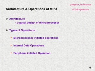
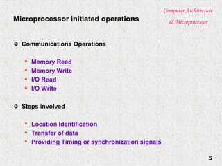
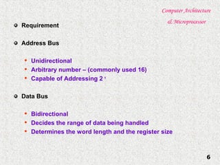
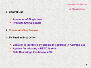
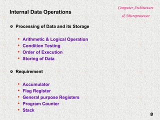
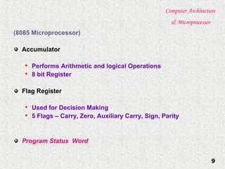
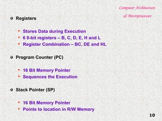
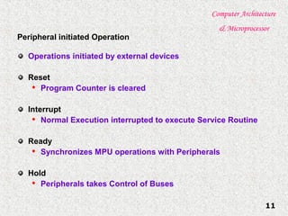
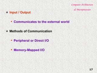
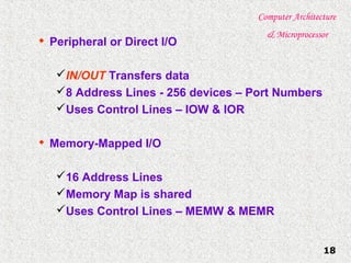
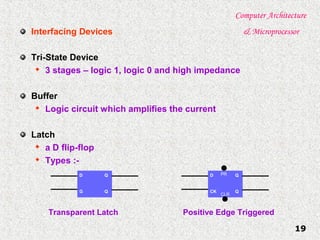
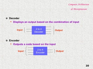
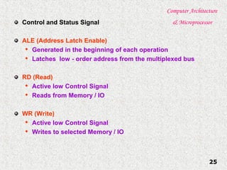
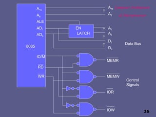
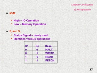
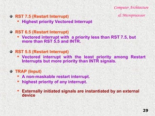
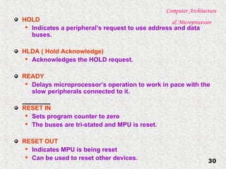
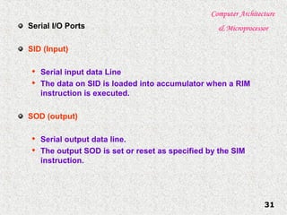
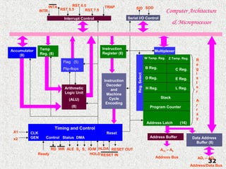
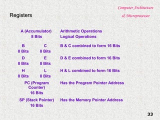
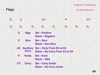
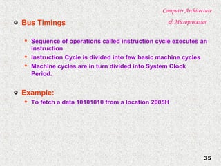
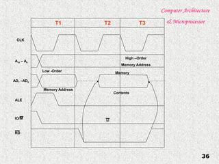
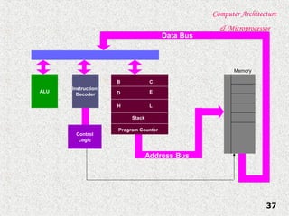
Computer Architecture
& Microprocessor
1
Computer Architecture and
MicroProcessor
Unit-2
Dr. V.Umadevi M.Sc(CS &IT). M.Tech (IT)., M.Phil., PhD., D.Litt.,
Director, Department of Computer Science, Jairams Arts and
Science College, Karur.
2
Session IISession II
 Microprocessor – an Introduction
 General Architecture of Microprocessor
 Memory
 I/O
 Architecture of 8085 Microprocessor
Computer Architecture
& Microprocessor
3
Microprocessor – An IntroductionMicroprocessor – An Introduction
Programmable Logical device
Functionality

manipulates data

Controls timing of various operations

communicates with peripherals
Applications

Automation & Control
Computer Architecture
& Microprocessor
4
Architecture & Operations of MPUArchitecture & Operations of MPU
Architecture
- Logical design of microprocessor
Types of Operations

Microprocessor initiated operations

Internal Data Operations

Peripheral initiated Operation
Computer Architecture
& Microprocessor
5
Microprocessor initiated operationsMicroprocessor initiated operations
Communications Operations

Memory Read

Memory Write

I/O Read

I/O Write
Steps involved

Location Identification

Transfer of data

Providing Timing or synchronization signals
Computer Architecture
& Microprocessor
6
Requirement
Address Bus

Unidirectional

Arbitrary number – (commonly used 16)

Capable of Addressing 2 n
Data Bus

Bidirectional

Decides the range of data being handled

Determines the word length and the register size
Computer Architecture
& Microprocessor
7
Control Bus

A number of Single lines

Provides timing signals
Communication Process
To Read an instruction

Location is identified by placing the address in Address Bus

A pulse for initiating a READ is sent

Data Bus brings the data to MPU
Computer Architecture
& Microprocessor
8
Internal Data Operations
Processing of Data and its Storage

Arithmetic & Logical Operation

Condition Testing

Order of Execution

Storing of Data
Requirement

Accumulator

Flag Register

General purpose Registers

Program Counter

Stack
Computer Architecture
& Microprocessor
9
(8085 Microprocessor)
Accumulator

Performs Arithmetic and logical Operations

8 bit Register
Flag Register

Used for Decision Making

5 Flags – Carry, Zero, Auxiliary Carry, Sign, Parity
Program Status Word
Computer Architecture
& Microprocessor
10
Registers

Stores Data during Execution

6 8-bit registers – B, C, D, E, H and L

Register Combination – BC, DE and HL
Program Counter (PC)

16 Bit Memory Pointer

Sequences the Execution
Stack Pointer (SP)

16 Bit Memory Pointer

Points to location in R/W Memory
Computer Architecture
& Microprocessor
11
Peripheral initiated Operation
Operations initiated by external devices
Reset

Program Counter is cleared
Interrupt

Normal Execution interrupted to execute Service Routine
Ready

Synchronizes MPU operations with Peripherals
Hold

Peripherals takes Control of Buses
Computer Architecture
& Microprocessor
12
MemoryMemory
Stores Binary Values
Types

Read Write Memory (R/W M)

Read Only Memory (ROM)
R/W Memory (Random Access Memory)

Volatile

processes data

Types:- Static & Dynamic
Computer Architecture
& Microprocessor
13
Static R/W Memory

Flip-flops

Stored as Voltage
Dynamic R/W Memory

MOS Transistor

Stored as charges

Faster

Refreshing Circuit
Computer Architecture
& Microprocessor
14
ROM Memory

Non Volatile

Used for subroutines

Cheap & Dense

Types: -
Masked ROM
PROM (Programmable Read Only Memory)
EPROM (Erasable Programmable Read Only Memory)
EEPROM (Electrically Erasable PROM)
Computer Architecture
& Microprocessor
15
Memory Organization
A memory requires:

Chips containing Registers

Chip Select line

R/W line

Address lines

I/O lines
Memory Map

Assigning a unique address for each register
Computer Architecture
& Microprocessor
16
Control Logic
A
D
D
R
E
S
S
D
E
C
O
D
E
R
R/W
D7 D6 D5 D4 D3 D2 D1 D0
A2
A1
A0
110
110
101
100
011
010
001
000
Size of Memory

Number of Register

Number of I/O lines
CS
Computer Architecture
& Microprocessor
17
Input / Output

Communicates to the external world
Methods of Communication

Peripheral or Direct I/O

Memory-Mapped I/O
Computer Architecture
& Microprocessor
18

Peripheral or Direct I/O
IN/OUT Transfers data
8 Address Lines - 256 devices – Port Numbers
Uses Control Lines – IOW & IOR

Memory-Mapped I/O
16 Address Lines
Memory Map is shared
Uses Control Lines – MEMW & MEMR
Computer Architecture
& Microprocessor
19
Interfacing Devices
Tri-State Device

3 stages – logic 1, logic 0 and high impedance
Buffer

Logic circuit which amplifies the current
Latch

a D flip-flop

Types :-
D
G
Q
Q
Transparent Latch Positive Edge Triggered
D
CK
Q
Q
PR
CLR
Computer Architecture
& Microprocessor
20
Decoder

Displays an output based on the combination of input
Encoder

Outputs a code based on the input
2 to 4
Decoder
2 to 4
Encoder
Output
Output
Input
Input
Computer Architecture
& Microprocessor
21
8085 Microprocessor8085 Microprocessor
Features

8 bit

Has 40 pins

Multiplexed Address/ Data Bus
Computer Architecture
& Microprocessor
22
8085
PINOUT
X1
X2
RESET OUT
SOD
SID
TRAP
RST 7.5
RST 6.5
RST 5.5
INTR
INTA
AD0
AD1
AD2
AD3
AD4
AD5
AD6
AD7
Vcc
HOLD
HLDA
CLK(OUT)
RESET IN
READY
IO/M
S1
RD
WR
ALE
S0
A15
A14
A13
A12
A11
A10
A9
A8
1
2
3
4
5
6
7
8
9
10
11
12
14
14
15
16
17
18
19
20
40
39
38
37
36
35
34
33
32
31
30
29
28
27
26
25
24
23
22
21
Computer Architecture
& Microprocessor
23
+5V GND
Serial
I/O
Ports
Interrupts
&
Externally
Initiated
Signals
External Signal
Acknowledgement
RESET CLK OUT
OUT
X1 X2 Vcc Vss
ALE
S0
S1
IO/M
RD
WR
SID
SOD
TRAP
RST 7.5
RST 6.5
RST 5.5
INTR
READY
HOLD
RESET IN
INTA
HLDA
High-Order
Address Bus
Multiplexed
Address/Dat
a Bus
A15
A8
AD7
AD0
Control
And
Status Signals
8085 Signals
Computer Architecture
& Microprocessor
24
8085 Microprocessor Signal Groups
Address Bus

UniDirectional

8 Higher Order Address Bus
Multiplexed Address/Data Bus

BiDirectional

Bus Multiplexing

Latching of Low - order Address Bus – ALE
Computer Architecture
& Microprocessor
25
Control and Status Signal
ALE (Address Latch Enable)

Generated in the beginning of each operation

Latches low - order address from the multiplexed bus
RD (Read)

Active low Control Signal

Reads from Memory / IO
WR (Write)

Active low Control Signal

Writes to selected Memory / IO
Computer Architecture
& Microprocessor
26
IO/M
RD
8085
WR
A15
A8
ALE
AD7
AD0
EN
LATCH
A15
A8
A7
A0
D7
D0
Data Bus
MEMR
MEMW
IOR
IOW
Control
Signals
Computer Architecture
& Microprocessor
27
IO/M

High – IO Operation

Low – Memory Operation
S1 and S0

Status Signal – rarely used

Identifies various operations
S1 So Desc.
0 0 HALT
0 1 WRITE
1 0 READ
1 1 FETCH
Computer Architecture
& Microprocessor
28
Power Supply and Clock Frequency

+5V power supply (Vcc)

3 MHz clock (X1 & X2)

CLK – Used as System Clock for other devices
Interrupts and Externally Initiated Operations

Interrupts transfer the program control to specific memory
location
INTR (Interrupt Request)

A general-purpose interrupt.
INTA (Interrupt Acknowledge)

Acknowledges an interrupt
Computer Architecture
& Microprocessor
29
RST 7.5 (Restart Interrupt)

Highest priority Vectored Interrupt
RST 6.5 (Restart Interrupt)

Vectored interrupt with a priority less than RST 7.5, but
more than RST 5.5 and INTR.
RST 5.5 (Restart Interrupt)

Vectored interrupt with the least priority among Restart
Interrupts but more priority than INTR signals.
TRAP (Input)

A non-maskable restart interrupt.

highest priority of any interrupt.

Externally initiated signals are instantiated by an external
device
Computer Architecture
& Microprocessor
30
HOLD

Indicates a peripheral’s request to use address and data
buses.
HLDA ( Hold Acknowledge)

Acknowledges the HOLD request.
READY

Delays microprocessor’s operation to work in pace with the
slow peripherals connected to it.
RESET IN

Sets program counter to zero

The buses are tri-stated and MPU is reset.
RESET OUT

Indicates MPU is being reset

Can be used to reset other devices.
Computer Architecture
& Microprocessor
31
Serial I/O Ports
SID (Input)

Serial input data Line

The data on SID is loaded into accumulator when a RIM
instruction is executed.
SOD (output)

Serial output data line.

The output SOD is set or reset as specified by the SIM
instruction.
Computer Architecture
& Microprocessor
32
Address Buffer
Accumulator
(8)
Temp
Reg. (8)
Arithmetic
Logic Unit
(ALU)
(8)
Instruction
Decoder
and
Machine
Cycle
Encoding
Flag (5)
Flip-flops
Instruction
Register (8)
W Temp. Reg. Z Temp. Reg.
B Reg.
D Reg.
H Reg.
Stack
Program Counter
C Reg.
E Reg.
L Reg.
Address Latch (16)
Data Address
Buffer (8)
Multiplexer
Timing and Control
CLK Reset
GEN Control Status DMA
Reg.Select
Serial I/O Control
SID
Interrupt Control
TRAP
RST 7.5
RST 6.5
RST 5.5
INTA
INTR
SOD
Ready
RD WR ALE S0 S1 IO/M HLDA RESET OUT
RESET INHOLD
A15 – A8
Address Bus AD7 – AD0
Address/Data Bus
X1
x2
R
e
g
i
s
t
e
r
A
r
r
a
y
Computer Architecture
& Microprocessor
33
RegistersRegisters
A (Accumulator)
8 Bits
Arithmetic Operations
Logical Operations
B
8 Bits
C
8 Bits
B & C combined to form 16 Bits
D
8 Bits
E
8 Bits
D & E combined to form 16 Bits
H
8 Bits
L
8 Bits
H & L combined to form 16 Bits
PC (Program
Counter)
16 Bits
Has the Program Pointer Address
SP (Stack Pointer)
16 Bits
Has the Memory Pointer Address
Computer Architecture
& Microprocessor
34
FlagsFlags
S Z AC P CY
D7 D6 D5 D4 D3 D2 D1 D0
S Sign Set – Positive
Reset – Negative
Z Zero Set – Zero
Reset – Non-Zero
AC Auxiliary
Carry
Set – Carry From D3 to D4
Reset – No Carry From D3 to D4
P Parity Set – Even
Reset – Odd
CY Carry Set – Carry Exists
Reset – No Carry exists
Computer Architecture
& Microprocessor
35
Bus Timings

Sequence of operations called instruction cycle executes an
instruction

Instruction Cycle is divided into few basic machine cycles

Machine cycles are in turn divided into System Clock
Period.
Example:

To fetch a data 10101010 from a location 2005H
Computer Architecture
& Microprocessor
36
T1 T2 T3
CLK
A15 – A8
AD7 –AD0
ALE
IO/M
RD
Low -Order
Memory Address
Memory
Contents
M
High –Order
Memory Address
Computer Architecture
& Microprocessor
37
ALU
Instruction
Decoder
Control
Logic
B
D
H
Stack
Program Counter
C
E
L
Address Bus
Data Bus
Memory

computer architecture

  • 1.
    Computer Architecture & Microprocessor 1 ComputerArchitecture and MicroProcessor Unit-2 Dr. V.Umadevi M.Sc(CS &IT). M.Tech (IT)., M.Phil., PhD., D.Litt., Director, Department of Computer Science, Jairams Arts and Science College, Karur.
  • 2.
    2 Session IISession II Microprocessor – an Introduction  General Architecture of Microprocessor  Memory  I/O  Architecture of 8085 Microprocessor
  • 3.
    Computer Architecture & Microprocessor 3 Microprocessor– An IntroductionMicroprocessor – An Introduction Programmable Logical device Functionality  manipulates data  Controls timing of various operations  communicates with peripherals Applications  Automation & Control
  • 4.
    Computer Architecture & Microprocessor 4 Architecture& Operations of MPUArchitecture & Operations of MPU Architecture - Logical design of microprocessor Types of Operations  Microprocessor initiated operations  Internal Data Operations  Peripheral initiated Operation
  • 5.
    Computer Architecture & Microprocessor 5 Microprocessorinitiated operationsMicroprocessor initiated operations Communications Operations  Memory Read  Memory Write  I/O Read  I/O Write Steps involved  Location Identification  Transfer of data  Providing Timing or synchronization signals
  • 6.
    Computer Architecture & Microprocessor 6 Requirement AddressBus  Unidirectional  Arbitrary number – (commonly used 16)  Capable of Addressing 2 n Data Bus  Bidirectional  Decides the range of data being handled  Determines the word length and the register size
  • 7.
    Computer Architecture & Microprocessor 7 ControlBus  A number of Single lines  Provides timing signals Communication Process To Read an instruction  Location is identified by placing the address in Address Bus  A pulse for initiating a READ is sent  Data Bus brings the data to MPU
  • 8.
    Computer Architecture & Microprocessor 8 InternalData Operations Processing of Data and its Storage  Arithmetic & Logical Operation  Condition Testing  Order of Execution  Storing of Data Requirement  Accumulator  Flag Register  General purpose Registers  Program Counter  Stack
  • 9.
    Computer Architecture & Microprocessor 9 (8085Microprocessor) Accumulator  Performs Arithmetic and logical Operations  8 bit Register Flag Register  Used for Decision Making  5 Flags – Carry, Zero, Auxiliary Carry, Sign, Parity Program Status Word
  • 10.
    Computer Architecture & Microprocessor 10 Registers  StoresData during Execution  6 8-bit registers – B, C, D, E, H and L  Register Combination – BC, DE and HL Program Counter (PC)  16 Bit Memory Pointer  Sequences the Execution Stack Pointer (SP)  16 Bit Memory Pointer  Points to location in R/W Memory
  • 11.
    Computer Architecture & Microprocessor 11 Peripheralinitiated Operation Operations initiated by external devices Reset  Program Counter is cleared Interrupt  Normal Execution interrupted to execute Service Routine Ready  Synchronizes MPU operations with Peripherals Hold  Peripherals takes Control of Buses
  • 12.
    Computer Architecture & Microprocessor 12 MemoryMemory StoresBinary Values Types  Read Write Memory (R/W M)  Read Only Memory (ROM) R/W Memory (Random Access Memory)  Volatile  processes data  Types:- Static & Dynamic
  • 13.
    Computer Architecture & Microprocessor 13 StaticR/W Memory  Flip-flops  Stored as Voltage Dynamic R/W Memory  MOS Transistor  Stored as charges  Faster  Refreshing Circuit
  • 14.
    Computer Architecture & Microprocessor 14 ROMMemory  Non Volatile  Used for subroutines  Cheap & Dense  Types: - Masked ROM PROM (Programmable Read Only Memory) EPROM (Erasable Programmable Read Only Memory) EEPROM (Electrically Erasable PROM)
  • 15.
    Computer Architecture & Microprocessor 15 MemoryOrganization A memory requires:  Chips containing Registers  Chip Select line  R/W line  Address lines  I/O lines Memory Map  Assigning a unique address for each register
  • 16.
    Computer Architecture & Microprocessor 16 ControlLogic A D D R E S S D E C O D E R R/W D7 D6 D5 D4 D3 D2 D1 D0 A2 A1 A0 110 110 101 100 011 010 001 000 Size of Memory  Number of Register  Number of I/O lines CS
  • 17.
    Computer Architecture & Microprocessor 17 Input/ Output  Communicates to the external world Methods of Communication  Peripheral or Direct I/O  Memory-Mapped I/O
  • 18.
    Computer Architecture & Microprocessor 18  Peripheralor Direct I/O IN/OUT Transfers data 8 Address Lines - 256 devices – Port Numbers Uses Control Lines – IOW & IOR  Memory-Mapped I/O 16 Address Lines Memory Map is shared Uses Control Lines – MEMW & MEMR
  • 19.
    Computer Architecture & Microprocessor 19 InterfacingDevices Tri-State Device  3 stages – logic 1, logic 0 and high impedance Buffer  Logic circuit which amplifies the current Latch  a D flip-flop  Types :- D G Q Q Transparent Latch Positive Edge Triggered D CK Q Q PR CLR
  • 20.
    Computer Architecture & Microprocessor 20 Decoder  Displaysan output based on the combination of input Encoder  Outputs a code based on the input 2 to 4 Decoder 2 to 4 Encoder Output Output Input Input
  • 21.
    Computer Architecture & Microprocessor 21 8085Microprocessor8085 Microprocessor Features  8 bit  Has 40 pins  Multiplexed Address/ Data Bus
  • 22.
    Computer Architecture & Microprocessor 22 8085 PINOUT X1 X2 RESETOUT SOD SID TRAP RST 7.5 RST 6.5 RST 5.5 INTR INTA AD0 AD1 AD2 AD3 AD4 AD5 AD6 AD7 Vcc HOLD HLDA CLK(OUT) RESET IN READY IO/M S1 RD WR ALE S0 A15 A14 A13 A12 A11 A10 A9 A8 1 2 3 4 5 6 7 8 9 10 11 12 14 14 15 16 17 18 19 20 40 39 38 37 36 35 34 33 32 31 30 29 28 27 26 25 24 23 22 21
  • 23.
    Computer Architecture & Microprocessor 23 +5VGND Serial I/O Ports Interrupts & Externally Initiated Signals External Signal Acknowledgement RESET CLK OUT OUT X1 X2 Vcc Vss ALE S0 S1 IO/M RD WR SID SOD TRAP RST 7.5 RST 6.5 RST 5.5 INTR READY HOLD RESET IN INTA HLDA High-Order Address Bus Multiplexed Address/Dat a Bus A15 A8 AD7 AD0 Control And Status Signals 8085 Signals
  • 24.
    Computer Architecture & Microprocessor 24 8085Microprocessor Signal Groups Address Bus  UniDirectional  8 Higher Order Address Bus Multiplexed Address/Data Bus  BiDirectional  Bus Multiplexing  Latching of Low - order Address Bus – ALE
  • 25.
    Computer Architecture & Microprocessor 25 Controland Status Signal ALE (Address Latch Enable)  Generated in the beginning of each operation  Latches low - order address from the multiplexed bus RD (Read)  Active low Control Signal  Reads from Memory / IO WR (Write)  Active low Control Signal  Writes to selected Memory / IO
  • 26.
  • 27.
    Computer Architecture & Microprocessor 27 IO/M  High– IO Operation  Low – Memory Operation S1 and S0  Status Signal – rarely used  Identifies various operations S1 So Desc. 0 0 HALT 0 1 WRITE 1 0 READ 1 1 FETCH
  • 28.
    Computer Architecture & Microprocessor 28 PowerSupply and Clock Frequency  +5V power supply (Vcc)  3 MHz clock (X1 & X2)  CLK – Used as System Clock for other devices Interrupts and Externally Initiated Operations  Interrupts transfer the program control to specific memory location INTR (Interrupt Request)  A general-purpose interrupt. INTA (Interrupt Acknowledge)  Acknowledges an interrupt
  • 29.
    Computer Architecture & Microprocessor 29 RST7.5 (Restart Interrupt)  Highest priority Vectored Interrupt RST 6.5 (Restart Interrupt)  Vectored interrupt with a priority less than RST 7.5, but more than RST 5.5 and INTR. RST 5.5 (Restart Interrupt)  Vectored interrupt with the least priority among Restart Interrupts but more priority than INTR signals. TRAP (Input)  A non-maskable restart interrupt.  highest priority of any interrupt.  Externally initiated signals are instantiated by an external device
  • 30.
    Computer Architecture & Microprocessor 30 HOLD  Indicatesa peripheral’s request to use address and data buses. HLDA ( Hold Acknowledge)  Acknowledges the HOLD request. READY  Delays microprocessor’s operation to work in pace with the slow peripherals connected to it. RESET IN  Sets program counter to zero  The buses are tri-stated and MPU is reset. RESET OUT  Indicates MPU is being reset  Can be used to reset other devices.
  • 31.
    Computer Architecture & Microprocessor 31 SerialI/O Ports SID (Input)  Serial input data Line  The data on SID is loaded into accumulator when a RIM instruction is executed. SOD (output)  Serial output data line.  The output SOD is set or reset as specified by the SIM instruction.
  • 32.
    Computer Architecture & Microprocessor 32 AddressBuffer Accumulator (8) Temp Reg. (8) Arithmetic Logic Unit (ALU) (8) Instruction Decoder and Machine Cycle Encoding Flag (5) Flip-flops Instruction Register (8) W Temp. Reg. Z Temp. Reg. B Reg. D Reg. H Reg. Stack Program Counter C Reg. E Reg. L Reg. Address Latch (16) Data Address Buffer (8) Multiplexer Timing and Control CLK Reset GEN Control Status DMA Reg.Select Serial I/O Control SID Interrupt Control TRAP RST 7.5 RST 6.5 RST 5.5 INTA INTR SOD Ready RD WR ALE S0 S1 IO/M HLDA RESET OUT RESET INHOLD A15 – A8 Address Bus AD7 – AD0 Address/Data Bus X1 x2 R e g i s t e r A r r a y
  • 33.
    Computer Architecture & Microprocessor 33 RegistersRegisters A(Accumulator) 8 Bits Arithmetic Operations Logical Operations B 8 Bits C 8 Bits B & C combined to form 16 Bits D 8 Bits E 8 Bits D & E combined to form 16 Bits H 8 Bits L 8 Bits H & L combined to form 16 Bits PC (Program Counter) 16 Bits Has the Program Pointer Address SP (Stack Pointer) 16 Bits Has the Memory Pointer Address
  • 34.
    Computer Architecture & Microprocessor 34 FlagsFlags SZ AC P CY D7 D6 D5 D4 D3 D2 D1 D0 S Sign Set – Positive Reset – Negative Z Zero Set – Zero Reset – Non-Zero AC Auxiliary Carry Set – Carry From D3 to D4 Reset – No Carry From D3 to D4 P Parity Set – Even Reset – Odd CY Carry Set – Carry Exists Reset – No Carry exists
  • 35.
    Computer Architecture & Microprocessor 35 BusTimings  Sequence of operations called instruction cycle executes an instruction  Instruction Cycle is divided into few basic machine cycles  Machine cycles are in turn divided into System Clock Period. Example:  To fetch a data 10101010 from a location 2005H
  • 36.
    Computer Architecture & Microprocessor 36 T1T2 T3 CLK A15 – A8 AD7 –AD0 ALE IO/M RD Low -Order Memory Address Memory Contents M High –Order Memory Address
  • 37.