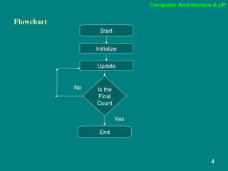
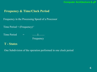
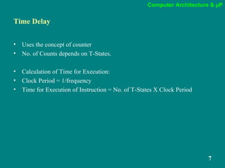
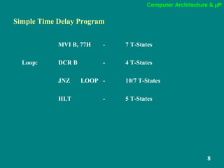
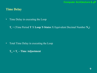
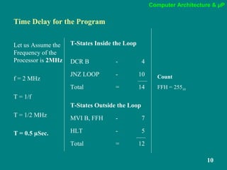
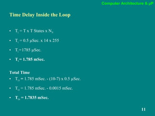
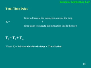
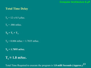
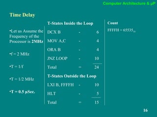
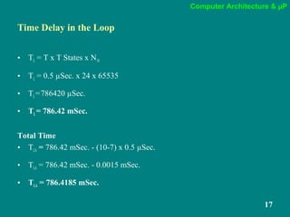
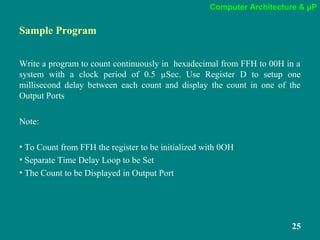
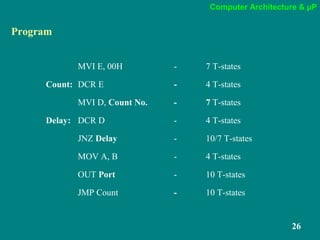
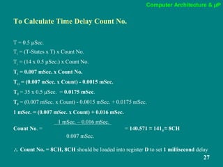
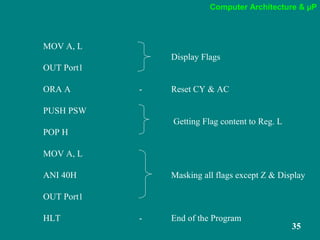
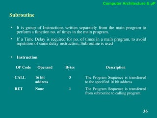
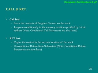
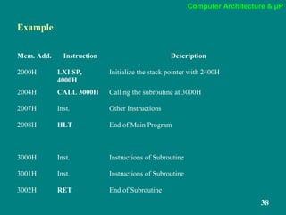
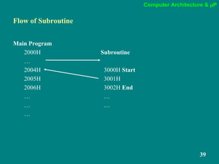
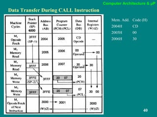
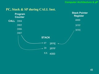
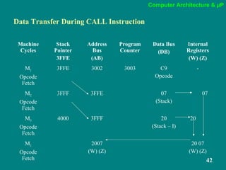
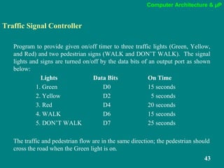
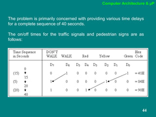
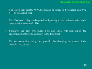
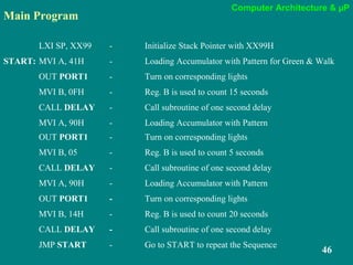
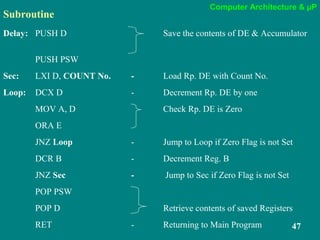
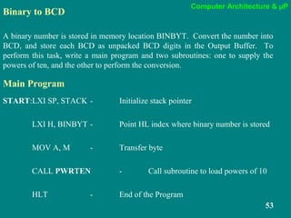
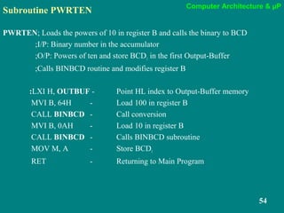
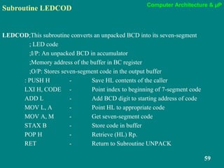
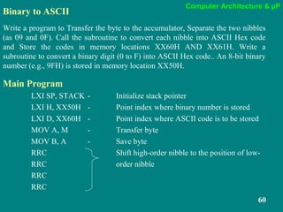
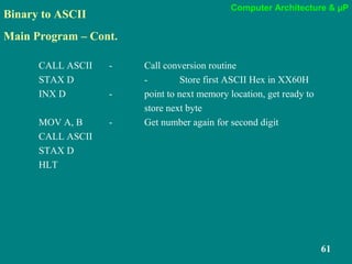
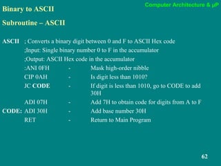
Computer Architecture & µP
1
CA & µP
Unit IV
Computer Architecture & µP
Computer Architecture and
MicroProcessor
Unit-4
Dr. V.Umadevi M.Sc(CS &IT). M.Tech (IT)., M.Phil., PhD.,
D.Litt.,
Director, Department of Computer Science, Jairams Arts and
Science College, Karur.
Computer Architecture & µP
3
Setting up a Counter
• Executes certain set of instructions a specified number of times
• A Register is Loaded with a number
• Using INR (Increment) or DCR (Decrement) the number is Incremented or
Decremented
• Uses the concept of conditional loop
• Time delay required
• If the register reaches the final count the loop is terminated
Computer Architecture & µP
4
Flowchart
Start
Initialize
Update
Is the
Final
Count
End
No
Yes
Computer Architecture & µP
5
Time Delay
Computer Architecture & µP
6
T - States
One Subdivision of the operation performed in one clock period
Frequency & Time/Clock Period
Frequency in the Processing Speed of a Processor
Time Period = (Frequency)-1
Time Period = 1
Frequency
Computer Architecture & µP
7
Time Delay
• Uses the concept of counter
• No. of Counts depends on T-States.
• Calculation of Time for Execution:
• Clock Period = 1/frequency
• Time for Execution of Instruction = No. of T-States X Clock Period
Computer Architecture & µP
8
Simple Time Delay Program
MVI B, 77H - 7 T-States
Loop: DCR B - 4 T-States
JNZ LOOP - 10/7 T-States
HLT - 5 T-States
Computer Architecture & µP
9
Time Delay
• Time Delay in executing the Loop
TL = (Time Period T X Loop T-States X Equivalent Decimal Number N10)
• Total Time Delay in executing the Loop
TLA = TL – Time Adjustment
Computer Architecture & µP
10
Time Delay for the Program
Let us Assume the
Frequency of the
Processor is 2MHz
f = 2 MHz
T = 1/f
T = 1/2 MHz
T = 0.5 µSec.
T-States Inside the Loop
DCR B - 4
JNZ LOOP - 10
Total = 14
T-States Outside the Loop
MVI B, FFH - 7
HLT - 5
Total = 12
Count
FFH = 25510
Computer Architecture & µP
11
Time Delay Inside the Loop
• TL = T x T States x N10
• TL = 0.5 µSec. x 14 x 255
• TL=1785 µSec.
• TL= 1.785 mSec.
Total Time
• TLA = 1.785 mSec. - (10-7) x 0.5 µSec.
• TLA = 1.785 mSec. - 0.0015 mSec.
• TLA = 1.7835 mSec.
Computer Architecture & µP
12
Total Time Delay
Time to Execute the instruction outside the loop
TD = +
Time taken to execute the instruction inside the loop
TD = TO + TLA
Where TO = T-States Outside the loop X Time Period
Computer Architecture & µP
13
Total Time Delay
TO = 12 x 0.5 µSec.
TO = .006 mSec.
TD = TO + TLA
TD = 0.006 mSec + 1.7835 mSec.
TD = 1.7895 mSec.
TD ≈ 1.8 mSec.
Total Time Required to execute the program is 1.8 milli Seconds (Approx.)
Computer Architecture & µP
14
Note:
• Time Delay can be Varied by changing the Count number FFH.
• To Increase the time delay more the 1.8 mSec. the user should use the
Additional Instruction or Register Pair.
Computer Architecture & µP
15
Time Delay Using Register Pair
Program
LXI B, FFFFH - 10 T-States
Loop: DCX B - 6 T-States
MOV A, C - 4 T-States
ORA B - 4 T-States
JNZ Loop - 10/7 T-States
HLT - 5 T-States
Computer Architecture & µP
16
Time Delay
•Let us Assume the
Frequency of the
Processor is 2MHz
•f = 2 MHz
•T = 1/f
•T = 1/2 MHz
•T = 0.5 µSec.
T-States Inside the Loop
DCX B - 6
MOV A,C - 4
ORA B - 4
JNZ LOOP - 10
Total = 24
T-States Outside the Loop
LXI B, FFFFH - 10
HLT - 5
Total = 15
Count
FFFFH = 6553510
Computer Architecture & µP
17
Time Delay in the Loop
• TL = T x T States x N10
• TL = 0.5 µSec. x 24 x 65535
• TL=786420 µSec.
• TL= 786.42 mSec.
Total Time
• TLA = 786.42 mSec. - (10-7) x 0.5 µSec.
• TLA = 786.42 mSec. - 0.0015 mSec.
• TLA = 786.4185 mSec.
Computer Architecture & µP
18
Total Time Delay
TO = 15 x 0.5 µSec.
TO = .0075 mSec.
TD = TO + TLA
TD = 0.0075 mSec + 786.4185 mSec.
TD = 786.426 mSec.
TD ≈ 786.4 mSec.
Total Time Required to execute the program is 786.4 milli Seconds (Approx.)
Computer Architecture & µP
19
Flowchart
Start
Initialize Loop2
Update
Is the Final
Count
End
Initialize Loop1
Update
Is the Final
Count
No
No
Yes
Yes
Computer Architecture & µP
20
Time Delay Using Loop within a Loop
Program
MVI B, FFH - 10 T-States
Loop2: MVI C, FFH - 10 T-States
Loop1: DCR C - 6 T-States
JNZ Loop1 - 10/7 T-States
DCR B - 6 T-States
JNZ Loop2 - 10/7 T-States
HLT - 5 T-States
L1 L2
Computer Architecture & µP
21
Time Delay
•Let us Assume the
Frequency of the
Processor is 2MHz
•f = 2 MHz
•T = 1/f
•T = 1/2 MHz
•T = 0.5 µSec.
T-States Inside the Loop1
DCR C - 4
JNZ Loop1 - 10
Total = 14
T-States Inside the Loop2
DCR C - 4
JNZ Loop1 - 7
DCR B - 4
JNZ Loop2 - 10
Total = 21
Count
Loop1 Count = FFH = 25510
Loop2 Count = FFH = 25510
T-States Outside the Loops
MVI B, FFH - 7
MVI C, FFH - 7
HLT - 5
Total = 19
Computer Architecture & µP
22
Time Delay in the Loop1
• TL1 = T x T States x N10
• TL1 = 0.5 µSec. x 14 x 255
• TL1=1785 µSec.
• TL1= 1.785 mSec.
Total Time
• TLA1 = 1.785 mSec. - (10-7) x 0.5 µSec.
• TLA1 = 1.785 mSec. - 0.0015 mSec.
• TLA1 = 1.7835 mSec.
Computer Architecture & µP
23
Time Delay in the Loop2
TL2 = (TLA1 + T-States X Time Period) X Count N10
• TL2 = (1.7835 mSec. + 21 x 0.5 µSec.) x 255
• TL2=457470 µSec.
• TL2= 457.47 mSec.
Total Time
• TLA2 = 457.47 mSec. - (10-7) x 0.5 µSec.
• TLA1 = 457.47 mSec. - 0.0015 mSec.
• TLA1 = 457.4685 mSec.
Computer Architecture & µP
24
Total Time Delay
TO = 19 x 0.5 µSec.
TO = .0095 mSec.
TD = TO + TLA2
TD = 0.0095 mSec + 457.4685 mSec.
TD = 457.478 mSec.
TD ≈ 457.5 mSec.
Total Time Required to execute the program is 457.5 milli Seconds (Approx.)
Computer Architecture & µP
25
Sample Program
Write a program to count continuously in hexadecimal from FFH to 00H in a
system with a clock period of 0.5 µSec. Use Register D to setup one
millisecond delay between each count and display the count in one of the
Output Ports
Note:
• To Count from FFH the register to be initialized with 0OH
• Separate Time Delay Loop to be Set
• The Count to be Displayed in Output Port
Computer Architecture & µP
26
Program
MVI E, 00H - 7 T-states
Count: DCR E - 4 T-states
MVI D, Count No. - 7 T-states
Delay: DCR D - 4 T-states
JNZ Delay - 10/7 T-states
MOV A, B - 4 T-states
OUT Port - 10 T-states
JMP Count - 10 T-states
Computer Architecture & µP
27
To Calculate Time Delay Count No.
T = 0.5 µSec.
TL = (T-States x T) x Count No.
TL = (14 x 0.5 µSec.) x Count No.
TL = 0.007 mSec. x Count No.
TLA = (0.007 mSec. x Count) - 0.0015 mSec.
TO = 35 x 0.5 µSec. = 0.0175 mSec.
TD = (0.007 mSec. x Count) - 0.0015 mSec. + 0.0175 mSec.
1 mSec. = (0.007 mSec. x Count) + 0.016 mSec.
1 mSec. – 0.016 mSec.
Count No. = = 140.571 ≈ 14110 ≈ 8CH
0.007 mSec.
∴ Count No. = 8CH, 8CH should be loaded into register D to set 1 millisecond delay
Computer Architecture & µP
28
Stack
• Set of Memory Locations in R/W memory
• Used to store binary information temporarily during the execution of a
program
• Beginning of Stack is defined using
LXI SP, 16 bit Address
• Stack pointer is decremented by one
• The byte stored to stack with the address specified in Stack Pointer
• The Storage & Retrieval on stack follows LIFO (Last in First Out)
Computer Architecture & µP
29
Storing Register Pair Content to Stack
• Using Inst. PUSH the contents of a Register Pair can be copied to stack
• Using Inst. POP the contents from the stack is copied to Register Pair
OP Code Operand Bytes Description
PUSH Rp. 1 Decrement the Stack Pointer by one
the content of higher order (B, D, H,
A) is copied into stack then the Stack
Pointer is again decremented the lower
order (C, E, L, Flags) is copied into
stack
POP Rp. 1 Copy the content of the stack which is
pointer by stack pointer to lower order
register (C, E, L, Flags) and
increment the stack pointer by one
then Copy the content of the stack
which is pointer by stack pointer to
higher order register (B, D, H, A)
Computer Architecture & µP
30
Stack Instructions
PUSH B - From Rp. BC to Stack
PUSH D - From Rp. DE to Stack
PUSH H - From Rp. HL to Stack
PUSH PSW - From Accumulator & Flags to Stack
POP B - From Stack to Rp. BC
POP D - From Stack to Rp. DE
POP H - From Stack to Rp. HL
POP PSW - From Stack to Accumulator & Flags
Note: PSW stands for Program Status Word
Computer Architecture & µP
31
Example:
Program:
1 LXI SP, 2000H
2 LXI H, 4253H
3 PUSH H
4 NOP
5 POP B
6 HLT
Computer Architecture & µP
32
Register Contents after executing first 2 Instructions
XX
2000
5342
A
B
D
H
SP
Register Contents after executing PUSH Instructions
XX
2000
5342
X
42
53
Memory
A
B
D 1FFE
H 1FFF
SP 2000
Computer Architecture & µP
33
Register Contents after executing POP Instructions
5342
2000
5342
X
42
53
Memory
A Flags
B C
D E
H L
SP
Computer Architecture & µP
34
• Program to Clear all Flags , Load 00H in the accumulator and demonstrate
the zero flag is not affected by data transfer instruction. Logically OR the
accumulator with itself to set the zero flag, and display the flag at Port1 or
store all the flags on the stack.
LXI SP, 2000H - Initialize Stack Pointer
MVI L, 00H
PUSH H To Clear Flags
POP PSW
MVI A, 00H - Loading Accumulator with 00H
A Data Transfer Instruction
PUSH PSW
Getting Flag content to Reg. L
POP H
Computer Architecture & µP
35
MOV A, L
Display Flags
OUT Port1
ORA A - Reset CY & AC
PUSH PSW
Getting Flag content to Reg. L
POP H
MOV A, L
ANI 40H Masking all flags except Z & Display
OUT Port1
HLT - End of the Program
Computer Architecture & µP
36
Subroutine
• It is group of Instructions written separately from the main program to
perform a function no. of times in the main program.
• If a Time Delay is required for no. of times in a main program, to avoid
repetition of same delay instruction, Subroutine is used
• Instruction
OP Code Operand Bytes Description
CALL 16 bit
address
3 The Program Sequence is transferred
to the specified 16 bit address
RET None 1 The Program Sequence is transferred
from subroutine to calling program.
Computer Architecture & µP
37
CALL & RET
• Call Inst.
– Saves the contents of Program Counter on the stack
– Jumps unconditionally to the memory location specified by 16 bit
address (Note: Conditional Call Statements are also there)
• RET inst.
– Copies the content in the top two location of the stack
– Unconditional Return from Subroutine (Note: Conditional Return
Statements are also there)
Computer Architecture & µP
38
Example
Mem. Add. Instruction Description
2000H LXI SP,
4000H
Initialize the stack pointer with 2400H
2004H CALL 3000H Calling the subroutine at 3000H
2007H Inst. Other Instructions
2008H HLT End of Main Program
3000H Inst. Instructions of Subroutine
3001H Inst. Instructions of Subroutine
3002H RET End of Subroutine
Computer Architecture & µP
39
Flow of Subroutine
Main Program
2000H Subroutine
…
2004H 3000H Start
2005H 3001H
2006H 3002H End
… …
… …
…
Computer Architecture & µP
40
Data Transfer During CALL Instruction
Mem. Add. Code (H)
2004H CD
2005H 00
2006H 30
Computer Architecture & µP
41
PC, Stack & SP during CALL Inst.
2004
2005
2006
2007
07
20
XX
CALL 4000
3FFF
3FFE
Program
Counter
Stack Pointer
Register
3FFE
3FFF
4000
STACK
Computer Architecture & µP
42
Data Transfer During CALL Instruction
Machine
Cycles
Stack
Pointer
3FFE
Address
Bus
(AB)
Program
Counter
Data Bus
(DB)
Internal
Registers
(W) (Z)
M1
Opcode
Fetch
3FFE 3002 3003 C9
Opcode
-
M2
Opcode
Fetch
3FFF 3FFE 07
(Stack)
07
M3
Opcode
Fetch
4000 3FFF 20
(Stack – I)
20
M1
Opcode
Fetch
2007
(W) (Z)
20 07
(W) (Z)
Computer Architecture & µP
43
Traffic Signal Controller
Program to provide given on/off timer to three traffic lights (Green, Yellow,
and Red) and two pedestrian signs (WALK and DON’T WALK). The signal
lights and signs are turned on/off by the data bits of an output port as shown
below:
Lights Data Bits On Time
1. Green D0 15 seconds
2. Yellow D2 5 seconds
3. Red D4 20 seconds
4. WALK D6 15 seconds
5. DON’T WALK D7 25 seconds
The traffic and pedestrian flow are in the same direction; the pedestrian should
cross the road when the Green light is on.
Computer Architecture & µP
44
The problem is primarily concerned with providing various time delays
for a complete sequence of 40 seconds.
The on/off times for the traffic signals and pedestrian signs are as
follows:
Computer Architecture & µP
45
• The Green light and the WALK sign can be turned on by sending data byte
41H to the output port.
• The 15-second delay can be provided by using a 1-second subroutine and a
counter with a count of 1510.
• Similarly, the next two bytes, 84H and 90H, will turn on/off the
appropriate lights/signs as shown in the flowchart.
• The necessary time delays are provided by changing the values of the
count in the counter.
Computer Architecture & µP
46
Main Program
LXI SP, XX99 - Initialize Stack Pointer with XX99H
START: MVI A, 41H - Loading Accumulator with Pattern for Green & Walk
OUT PORT1 - Turn on corresponding lights
MVI B, 0FH - Reg. B is used to count 15 seconds
CALL DELAY - Call subroutine of one second delay
MVI A, 90H - Loading Accumulator with Pattern
OUT PORT1 - Turn on corresponding lights
MVI B, 05 - Reg. B is used to count 5 seconds
CALL DELAY - Call subroutine of one second delay
MVI A, 90H - Loading Accumulator with Pattern
OUT PORT1 - Turn on corresponding lights
MVI B, 14H - Reg. B is used to count 20 seconds
CALL DELAY - Call subroutine of one second delay
JMP START - Go to START to repeat the Sequence
Computer Architecture & µP
47
Subroutine
Delay: PUSH D Save the contents of DE & Accumulator
PUSH PSW
Sec: LXI D, COUNT No. - Load Rp. DE with Count No.
Loop: DCX D - Decrement Rp. DE by one
MOV A, D Check Rp. DE is Zero
ORA E
JNZ Loop - Jump to Loop if Zero Flag is not Set
DCR B - Decrement Reg. B
JNZ Sec - Jump to Sec if Zero Flag is not Set
POP PSW
POP D Retrieve contents of saved Registers
RET - Returning to Main Program
Computer Architecture & µP
48
BCD – Binary Coded Decimal
• 8610= (8 x 10) + 2
• Converting a 2-digit BCD number into its binary equivalent requires the
following steps:
– Separate an 8-bit packed BCD number into two 4-bit unpacked BCD
digits: BCD1 and BCD2.
– Convert each digit into its binary value according to its position.
– Add both binary numbers to obtain the binary equivalent of the BCD
number.
Computer Architecture & µP
49
Example
• Convert (86)BCD into its binary equivalent
Solution: 8610 = 1000 0110 BCD
• 0111 0010
– 00000110 Unpacked BCD1
– 00001000 Unpacked BCD2
• Multiply BCD2 by 10 (8 x 10)
• Add BCD1 to the answer in Step 2.
Computer Architecture & µP
50
2 Digit BCD to Binary Conversion
A BCD number between 0 and 99 is stored in a R/W memory location called the Input
Buffer. Write a main program and a conversion subroutine (BCDBIN) to convert the BCD
number into its equivalent binary number. Store the result in a memory location defined as
the Output Buffer.
LXI SP, “STACK” - Initialize stack
LXI H, “INBUF” - Initialize Input Location
LXI B, “OUTBUF” - Initialize Output Location
MOV A, M - Input of BCD No.
CALL BCDBIN - Calling Subroutine
STAX B - Storing Binary No. to Output Buf.
HLT - End of the Program
Main Program
Computer Architecture & µP
51
Subroutine
BCDBIN; BCD to Binary
; I/P: packed BCD in Acc.
; O/P: Binary in Acc.
PUSH B - Save Rp.
MOV B, A - Copies Acc. Contents to Reg. B
ANI 0FH - ANDing (A) with 0FH to mask MSB
MOV C, A - Copies Acc. Contents to Reg. C
MOV A, B - Copies Reg. B contents to Acc.
ANI F0H - ANDing (A) with F0H to mask LSB
RRC
RRC Making MSB as LSB
RRC
RRC
MOV D, A - Copies Acc. Contents to Reg. D
XRA A - Clearing Acc. & Flags
Cont.
Computer Architecture & µP
52
MVI E, 0AH - Load Reg. E with 0AH = 1010
Sum: ADD E - Add (E) to (A)
DCR D - Decrement (D) by one
JNZ Sum - Jump to location Sum in Zero flag is reset
ADD C - Add (C) to (A)
POP B - Retrieve (BC)
RET - Returning to Main Program
Cont.
Computer Architecture & µP
53
Binary to BCD
A binary number is stored in memory location BINBYT. Convert the number into
BCD, and store each BCD as unpacked BCD digits in the Output Buffer. To
perform this task, write a main program and two subroutines: one to supply the
powers of ten, and the other to perform the conversion.
Main Program
START:LXI SP, STACK - Initialize stack pointer
LXI H, BINBYT - Point HL index where binary number is stored
MOV A, M - Transfer byte
CALL PWRTEN - Call subroutine to load powers of 10
HLT - End of the Program
Computer Architecture & µP
54
Subroutine PWRTEN
PWRTEN; Loads the powers of 10 in register B and calls the binary to BCD
;I/P: Binary number in the accumulator
;O/P: Powers of ten and store BCD1 in the first Output-Buffer
;Calls BINBCD routine and modifies register B
:LXI H, OUTBUF - Point HL index to Output-Buffer memory
MVI B, 64H - Load 100 in register B
CALL BINBCD - Call conversion
MVI B, 0AH - Load 10 in register B
CALL BINBCD - Calls BINBCD subroutine
MOV M, A - Store BCD1
RET - Returning to Main Program
Computer Architecture & µP
55
Subroutine BINBCD
BINBCD ;Converts a binary number into BCD and stores BCD2 and
;BCD3 in the Out put Buffer.
;I/P: Binary number in accumulator and powers of 10 in B
;O/P: BCD2 and BCD3 in Output Buffer
;Modifies accumulator contents
:MVI M, FFH - Load buffer with (0 -1)
NB: INR M - Clear buffer and increment for each subtraction
SUB B - Subtract power of 10 from binary number
JNC NB - Is number > power of 10? If yes, add 1 to buffer
ADD B - If no, add power of 10 to get remainder
INX H - Go to next buffer location
RET - Returning to Subroutine PWRTEN
Computer Architecture & µP
56
BCD to 7 Segment Display
Write a main program and two subroutines, called UNPAK and LEDCOD, to
unpack the BCD numbers and select an appropriate seven-segment code for each
digit. The codes should be stored in the Output-Buffer memory.
Main Program
LXI SP, STACK - Initialize stack pointer
LXI H, XX50H - Point HL index where BCD digits are stored
MVI D, 03H - Number of digits to be converted is placed in
D
CALL UNPAK - Call subroutine to unpack BCD numbers
HLT - End of Program
Computer Architecture & µP
57
Subroutine UNPACK
UNPAK;This subroutine unpacks the BCD number into two single digits.
;I/P: Starting memory address of the packed BCD numbers in HL
;registers: Number of BCDs to be converted in register D
;O/P: Unpacked BCD into acc. and Output Buffer address in BC
;Calls subroutine LEDCOD
LXI B, BUFFER - Point BC index to the buffer memory
NBCD: MOV A, M - Get packed BCD number
ANI F0H - Masked BCD1
RRC Rotate four times to place BCD2 as
RRC unpacked single digit BCD
RRC
RRC
Computer Architecture & µP
58
Subroutine UNPACK
CALL LEDCOD - Find seven-segment code
INX B - Point to next buffer location
MOV A, M - Get BCD number again
ANI 0FH - Separate BCD1
CALL LEDCOD -
INX B -
INX H - Point to next BCD
DCR D - Conversion complete, reduce BCD count
JNZ NBCD - If all BCDs are not yet converted, go back
to convert next
RET - Return to Main Program
Computer Architecture & µP
59
Subroutine LEDCOD
LEDCOD;This subroutine converts an unpacked BCD into its seven-segment
; LED code
;I/P: An unpacked BCD in accumulator
;Memory address of the buffer in BC register
;O/P: Stores seven-segment code in the output buffer
: PUSH H - Save HL contents of the caller
LXI H, CODE - Point index to beginning of 7-segment code
ADD L - Add BCD digit to starting address of code
MOV L, A - Point HL to appropriate code
MOV A, M - Get seven-segment code
STAX B - Store code in buffer
POP H - Retrieve (HL) Rp.
RET - Return to Subroutine UNPACK
Computer Architecture & µP
60
Binary to ASCII
Write a program to Transfer the byte to the accumulator, Separate the two nibbles
(as 09 and 0F). Call the subroutine to convert each nibble into ASCII Hex code
and Store the codes in memory locations XX60H AND XX61H. Write a
subroutine to convert a binary digit (0 to F) into ASCII Hex code.. An 8-bit binary
number (e.g., 9FH) is stored in memory location XX50H.
Main Program
LXI SP, STACK - Initialize stack pointer
LXI H, XX50H - Point index where binary number is stored
LXI D, XX60H - Point index where ASCII code is to be stored
MOV A, M - Transfer byte
MOV B, A - Save byte
RRC Shift high-order nibble to the position of low-
RRC order nibble
RRC
RRC
Computer Architecture & µP
61
Binary to ASCII
Main Program – Cont.
CALL ASCII - Call conversion routine
STAX D - Store first ASCII Hex in XX60H
INX D - point to next memory location, get ready to
store next byte
MOV A, B - Get number again for second digit
CALL ASCII
STAX D
HLT
Computer Architecture & µP
62
Binary to ASCII
Subroutine – ASCII
ASCII ; Converts a binary digit between 0 and F to ASCII Hex code
;Input: Single binary number 0 to F in the accumulator
;Output: ASCII Hex code in the accumulator
:ANI 0FH - Mask high-order nibble
CIP 0AH - Is digit less than 1010?
JC CODE - If digit is less than 1010, go to CODE to add
30H
ADI 07H - Add 7H to obtain code for digits from A to F
CODE: ADI 30H - Add base number 30H
RET - Return to Main Program
Computer Architecture & µP
63
ASCII to Binary
Write a subroutine to convert an ASCII Hex number into its binary equivalent. A
calling program places the ASCII number in the accumulator, and the subroutine
should pass the conversion back to the accumulator.
Subroutine
ASCBIN;This subroutine converts an ASCII Hex number into its binary
;Input: ASCII Hex number in the accumulator
;Output: Binary equivalent in the accumulator
:SUI 30H - Subtract 0 bias from the number
CPI 0AH - Check whether number is between 0 and 9
RC - If yes, return to main program
SUI 07H - If not, sub. 7 to find number between
A & F
RET - Return to Main Program
Computer Architecture & µP
64
BCD Multiplication
A multiplicand is stored in memory location XX50H and a multiplier is stored in
location XX51H. Write a main program to transfer the two numbers from memory
locations to the HL registers and store the product in the Output Buffer at XX90H.
Write a subroutine to Multiply two unsigned numbers placed in registers H and L
and Return the result into the HL pair.
Main Program
LXI SP, STACK
LHLD XX50H - Place contents of XX50 in L register and
contents of XX51 in H register
XCHG - Place multiplier in D and multiplicand in E
CALL MLTPLY - Multiply the two numbers
SHLD XX90H - Store the product in locations XX90 and 91H
HLT - End of the Program
Computer Architecture & µP
65
BCD Multiplication
Subroutine - MLTPLY
MLTPLY:MOV A, D - Transfer multiplier to accumulator
MVI D, 00H - Clear D to use in DAD instruction
LXI H, 0000H - Clear HL
MVI B, 08H - Set up register B to count eight rotations
NXTBIT:RAR - Check if multiplier bit is 1
JNC NOADD - If not, skip adding multiplicand
DAD D - If multiplier is 1, add multiplicand to HL and
place partial result in HL
NOADD:XCHG - Place multiplicand in HL
DAD H - And shift left
XCHG - Retrieve shifted multiplication
DCR B - One operation is complete, decrement counter
JNZ NXTBIT - Go back to next bit
RET - Return To Main Program

computer architecture 4

  • 1.
    Computer Architecture &µP 1 CA & µP Unit IV
  • 2.
    Computer Architecture &µP Computer Architecture and MicroProcessor Unit-4 Dr. V.Umadevi M.Sc(CS &IT). M.Tech (IT)., M.Phil., PhD., D.Litt., Director, Department of Computer Science, Jairams Arts and Science College, Karur.
  • 3.
    Computer Architecture &µP 3 Setting up a Counter • Executes certain set of instructions a specified number of times • A Register is Loaded with a number • Using INR (Increment) or DCR (Decrement) the number is Incremented or Decremented • Uses the concept of conditional loop • Time delay required • If the register reaches the final count the loop is terminated
  • 4.
    Computer Architecture &µP 4 Flowchart Start Initialize Update Is the Final Count End No Yes
  • 5.
    Computer Architecture &µP 5 Time Delay
  • 6.
    Computer Architecture &µP 6 T - States One Subdivision of the operation performed in one clock period Frequency & Time/Clock Period Frequency in the Processing Speed of a Processor Time Period = (Frequency)-1 Time Period = 1 Frequency
  • 7.
    Computer Architecture &µP 7 Time Delay • Uses the concept of counter • No. of Counts depends on T-States. • Calculation of Time for Execution: • Clock Period = 1/frequency • Time for Execution of Instruction = No. of T-States X Clock Period
  • 8.
    Computer Architecture &µP 8 Simple Time Delay Program MVI B, 77H - 7 T-States Loop: DCR B - 4 T-States JNZ LOOP - 10/7 T-States HLT - 5 T-States
  • 9.
    Computer Architecture &µP 9 Time Delay • Time Delay in executing the Loop TL = (Time Period T X Loop T-States X Equivalent Decimal Number N10) • Total Time Delay in executing the Loop TLA = TL – Time Adjustment
  • 10.
    Computer Architecture &µP 10 Time Delay for the Program Let us Assume the Frequency of the Processor is 2MHz f = 2 MHz T = 1/f T = 1/2 MHz T = 0.5 µSec. T-States Inside the Loop DCR B - 4 JNZ LOOP - 10 Total = 14 T-States Outside the Loop MVI B, FFH - 7 HLT - 5 Total = 12 Count FFH = 25510
  • 11.
    Computer Architecture &µP 11 Time Delay Inside the Loop • TL = T x T States x N10 • TL = 0.5 µSec. x 14 x 255 • TL=1785 µSec. • TL= 1.785 mSec. Total Time • TLA = 1.785 mSec. - (10-7) x 0.5 µSec. • TLA = 1.785 mSec. - 0.0015 mSec. • TLA = 1.7835 mSec.
  • 12.
    Computer Architecture &µP 12 Total Time Delay Time to Execute the instruction outside the loop TD = + Time taken to execute the instruction inside the loop TD = TO + TLA Where TO = T-States Outside the loop X Time Period
  • 13.
    Computer Architecture &µP 13 Total Time Delay TO = 12 x 0.5 µSec. TO = .006 mSec. TD = TO + TLA TD = 0.006 mSec + 1.7835 mSec. TD = 1.7895 mSec. TD ≈ 1.8 mSec. Total Time Required to execute the program is 1.8 milli Seconds (Approx.)
  • 14.
    Computer Architecture &µP 14 Note: • Time Delay can be Varied by changing the Count number FFH. • To Increase the time delay more the 1.8 mSec. the user should use the Additional Instruction or Register Pair.
  • 15.
    Computer Architecture &µP 15 Time Delay Using Register Pair Program LXI B, FFFFH - 10 T-States Loop: DCX B - 6 T-States MOV A, C - 4 T-States ORA B - 4 T-States JNZ Loop - 10/7 T-States HLT - 5 T-States
  • 16.
    Computer Architecture &µP 16 Time Delay •Let us Assume the Frequency of the Processor is 2MHz •f = 2 MHz •T = 1/f •T = 1/2 MHz •T = 0.5 µSec. T-States Inside the Loop DCX B - 6 MOV A,C - 4 ORA B - 4 JNZ LOOP - 10 Total = 24 T-States Outside the Loop LXI B, FFFFH - 10 HLT - 5 Total = 15 Count FFFFH = 6553510
  • 17.
    Computer Architecture &µP 17 Time Delay in the Loop • TL = T x T States x N10 • TL = 0.5 µSec. x 24 x 65535 • TL=786420 µSec. • TL= 786.42 mSec. Total Time • TLA = 786.42 mSec. - (10-7) x 0.5 µSec. • TLA = 786.42 mSec. - 0.0015 mSec. • TLA = 786.4185 mSec.
  • 18.
    Computer Architecture &µP 18 Total Time Delay TO = 15 x 0.5 µSec. TO = .0075 mSec. TD = TO + TLA TD = 0.0075 mSec + 786.4185 mSec. TD = 786.426 mSec. TD ≈ 786.4 mSec. Total Time Required to execute the program is 786.4 milli Seconds (Approx.)
  • 19.
    Computer Architecture &µP 19 Flowchart Start Initialize Loop2 Update Is the Final Count End Initialize Loop1 Update Is the Final Count No No Yes Yes
  • 20.
    Computer Architecture &µP 20 Time Delay Using Loop within a Loop Program MVI B, FFH - 10 T-States Loop2: MVI C, FFH - 10 T-States Loop1: DCR C - 6 T-States JNZ Loop1 - 10/7 T-States DCR B - 6 T-States JNZ Loop2 - 10/7 T-States HLT - 5 T-States L1 L2
  • 21.
    Computer Architecture &µP 21 Time Delay •Let us Assume the Frequency of the Processor is 2MHz •f = 2 MHz •T = 1/f •T = 1/2 MHz •T = 0.5 µSec. T-States Inside the Loop1 DCR C - 4 JNZ Loop1 - 10 Total = 14 T-States Inside the Loop2 DCR C - 4 JNZ Loop1 - 7 DCR B - 4 JNZ Loop2 - 10 Total = 21 Count Loop1 Count = FFH = 25510 Loop2 Count = FFH = 25510 T-States Outside the Loops MVI B, FFH - 7 MVI C, FFH - 7 HLT - 5 Total = 19
  • 22.
    Computer Architecture &µP 22 Time Delay in the Loop1 • TL1 = T x T States x N10 • TL1 = 0.5 µSec. x 14 x 255 • TL1=1785 µSec. • TL1= 1.785 mSec. Total Time • TLA1 = 1.785 mSec. - (10-7) x 0.5 µSec. • TLA1 = 1.785 mSec. - 0.0015 mSec. • TLA1 = 1.7835 mSec.
  • 23.
    Computer Architecture &µP 23 Time Delay in the Loop2 TL2 = (TLA1 + T-States X Time Period) X Count N10 • TL2 = (1.7835 mSec. + 21 x 0.5 µSec.) x 255 • TL2=457470 µSec. • TL2= 457.47 mSec. Total Time • TLA2 = 457.47 mSec. - (10-7) x 0.5 µSec. • TLA1 = 457.47 mSec. - 0.0015 mSec. • TLA1 = 457.4685 mSec.
  • 24.
    Computer Architecture &µP 24 Total Time Delay TO = 19 x 0.5 µSec. TO = .0095 mSec. TD = TO + TLA2 TD = 0.0095 mSec + 457.4685 mSec. TD = 457.478 mSec. TD ≈ 457.5 mSec. Total Time Required to execute the program is 457.5 milli Seconds (Approx.)
  • 25.
    Computer Architecture &µP 25 Sample Program Write a program to count continuously in hexadecimal from FFH to 00H in a system with a clock period of 0.5 µSec. Use Register D to setup one millisecond delay between each count and display the count in one of the Output Ports Note: • To Count from FFH the register to be initialized with 0OH • Separate Time Delay Loop to be Set • The Count to be Displayed in Output Port
  • 26.
    Computer Architecture &µP 26 Program MVI E, 00H - 7 T-states Count: DCR E - 4 T-states MVI D, Count No. - 7 T-states Delay: DCR D - 4 T-states JNZ Delay - 10/7 T-states MOV A, B - 4 T-states OUT Port - 10 T-states JMP Count - 10 T-states
  • 27.
    Computer Architecture &µP 27 To Calculate Time Delay Count No. T = 0.5 µSec. TL = (T-States x T) x Count No. TL = (14 x 0.5 µSec.) x Count No. TL = 0.007 mSec. x Count No. TLA = (0.007 mSec. x Count) - 0.0015 mSec. TO = 35 x 0.5 µSec. = 0.0175 mSec. TD = (0.007 mSec. x Count) - 0.0015 mSec. + 0.0175 mSec. 1 mSec. = (0.007 mSec. x Count) + 0.016 mSec. 1 mSec. – 0.016 mSec. Count No. = = 140.571 ≈ 14110 ≈ 8CH 0.007 mSec. ∴ Count No. = 8CH, 8CH should be loaded into register D to set 1 millisecond delay
  • 28.
    Computer Architecture &µP 28 Stack • Set of Memory Locations in R/W memory • Used to store binary information temporarily during the execution of a program • Beginning of Stack is defined using LXI SP, 16 bit Address • Stack pointer is decremented by one • The byte stored to stack with the address specified in Stack Pointer • The Storage & Retrieval on stack follows LIFO (Last in First Out)
  • 29.
    Computer Architecture &µP 29 Storing Register Pair Content to Stack • Using Inst. PUSH the contents of a Register Pair can be copied to stack • Using Inst. POP the contents from the stack is copied to Register Pair OP Code Operand Bytes Description PUSH Rp. 1 Decrement the Stack Pointer by one the content of higher order (B, D, H, A) is copied into stack then the Stack Pointer is again decremented the lower order (C, E, L, Flags) is copied into stack POP Rp. 1 Copy the content of the stack which is pointer by stack pointer to lower order register (C, E, L, Flags) and increment the stack pointer by one then Copy the content of the stack which is pointer by stack pointer to higher order register (B, D, H, A)
  • 30.
    Computer Architecture &µP 30 Stack Instructions PUSH B - From Rp. BC to Stack PUSH D - From Rp. DE to Stack PUSH H - From Rp. HL to Stack PUSH PSW - From Accumulator & Flags to Stack POP B - From Stack to Rp. BC POP D - From Stack to Rp. DE POP H - From Stack to Rp. HL POP PSW - From Stack to Accumulator & Flags Note: PSW stands for Program Status Word
  • 31.
    Computer Architecture &µP 31 Example: Program: 1 LXI SP, 2000H 2 LXI H, 4253H 3 PUSH H 4 NOP 5 POP B 6 HLT
  • 32.
    Computer Architecture &µP 32 Register Contents after executing first 2 Instructions XX 2000 5342 A B D H SP Register Contents after executing PUSH Instructions XX 2000 5342 X 42 53 Memory A B D 1FFE H 1FFF SP 2000
  • 33.
    Computer Architecture &µP 33 Register Contents after executing POP Instructions 5342 2000 5342 X 42 53 Memory A Flags B C D E H L SP
  • 34.
    Computer Architecture &µP 34 • Program to Clear all Flags , Load 00H in the accumulator and demonstrate the zero flag is not affected by data transfer instruction. Logically OR the accumulator with itself to set the zero flag, and display the flag at Port1 or store all the flags on the stack. LXI SP, 2000H - Initialize Stack Pointer MVI L, 00H PUSH H To Clear Flags POP PSW MVI A, 00H - Loading Accumulator with 00H A Data Transfer Instruction PUSH PSW Getting Flag content to Reg. L POP H
  • 35.
    Computer Architecture &µP 35 MOV A, L Display Flags OUT Port1 ORA A - Reset CY & AC PUSH PSW Getting Flag content to Reg. L POP H MOV A, L ANI 40H Masking all flags except Z & Display OUT Port1 HLT - End of the Program
  • 36.
    Computer Architecture &µP 36 Subroutine • It is group of Instructions written separately from the main program to perform a function no. of times in the main program. • If a Time Delay is required for no. of times in a main program, to avoid repetition of same delay instruction, Subroutine is used • Instruction OP Code Operand Bytes Description CALL 16 bit address 3 The Program Sequence is transferred to the specified 16 bit address RET None 1 The Program Sequence is transferred from subroutine to calling program.
  • 37.
    Computer Architecture &µP 37 CALL & RET • Call Inst. – Saves the contents of Program Counter on the stack – Jumps unconditionally to the memory location specified by 16 bit address (Note: Conditional Call Statements are also there) • RET inst. – Copies the content in the top two location of the stack – Unconditional Return from Subroutine (Note: Conditional Return Statements are also there)
  • 38.
    Computer Architecture &µP 38 Example Mem. Add. Instruction Description 2000H LXI SP, 4000H Initialize the stack pointer with 2400H 2004H CALL 3000H Calling the subroutine at 3000H 2007H Inst. Other Instructions 2008H HLT End of Main Program 3000H Inst. Instructions of Subroutine 3001H Inst. Instructions of Subroutine 3002H RET End of Subroutine
  • 39.
    Computer Architecture &µP 39 Flow of Subroutine Main Program 2000H Subroutine … 2004H 3000H Start 2005H 3001H 2006H 3002H End … … … … …
  • 40.
    Computer Architecture &µP 40 Data Transfer During CALL Instruction Mem. Add. Code (H) 2004H CD 2005H 00 2006H 30
  • 41.
    Computer Architecture &µP 41 PC, Stack & SP during CALL Inst. 2004 2005 2006 2007 07 20 XX CALL 4000 3FFF 3FFE Program Counter Stack Pointer Register 3FFE 3FFF 4000 STACK
  • 42.
    Computer Architecture &µP 42 Data Transfer During CALL Instruction Machine Cycles Stack Pointer 3FFE Address Bus (AB) Program Counter Data Bus (DB) Internal Registers (W) (Z) M1 Opcode Fetch 3FFE 3002 3003 C9 Opcode - M2 Opcode Fetch 3FFF 3FFE 07 (Stack) 07 M3 Opcode Fetch 4000 3FFF 20 (Stack – I) 20 M1 Opcode Fetch 2007 (W) (Z) 20 07 (W) (Z)
  • 43.
    Computer Architecture &µP 43 Traffic Signal Controller Program to provide given on/off timer to three traffic lights (Green, Yellow, and Red) and two pedestrian signs (WALK and DON’T WALK). The signal lights and signs are turned on/off by the data bits of an output port as shown below: Lights Data Bits On Time 1. Green D0 15 seconds 2. Yellow D2 5 seconds 3. Red D4 20 seconds 4. WALK D6 15 seconds 5. DON’T WALK D7 25 seconds The traffic and pedestrian flow are in the same direction; the pedestrian should cross the road when the Green light is on.
  • 44.
    Computer Architecture &µP 44 The problem is primarily concerned with providing various time delays for a complete sequence of 40 seconds. The on/off times for the traffic signals and pedestrian signs are as follows:
  • 45.
    Computer Architecture &µP 45 • The Green light and the WALK sign can be turned on by sending data byte 41H to the output port. • The 15-second delay can be provided by using a 1-second subroutine and a counter with a count of 1510. • Similarly, the next two bytes, 84H and 90H, will turn on/off the appropriate lights/signs as shown in the flowchart. • The necessary time delays are provided by changing the values of the count in the counter.
  • 46.
    Computer Architecture &µP 46 Main Program LXI SP, XX99 - Initialize Stack Pointer with XX99H START: MVI A, 41H - Loading Accumulator with Pattern for Green & Walk OUT PORT1 - Turn on corresponding lights MVI B, 0FH - Reg. B is used to count 15 seconds CALL DELAY - Call subroutine of one second delay MVI A, 90H - Loading Accumulator with Pattern OUT PORT1 - Turn on corresponding lights MVI B, 05 - Reg. B is used to count 5 seconds CALL DELAY - Call subroutine of one second delay MVI A, 90H - Loading Accumulator with Pattern OUT PORT1 - Turn on corresponding lights MVI B, 14H - Reg. B is used to count 20 seconds CALL DELAY - Call subroutine of one second delay JMP START - Go to START to repeat the Sequence
  • 47.
    Computer Architecture &µP 47 Subroutine Delay: PUSH D Save the contents of DE & Accumulator PUSH PSW Sec: LXI D, COUNT No. - Load Rp. DE with Count No. Loop: DCX D - Decrement Rp. DE by one MOV A, D Check Rp. DE is Zero ORA E JNZ Loop - Jump to Loop if Zero Flag is not Set DCR B - Decrement Reg. B JNZ Sec - Jump to Sec if Zero Flag is not Set POP PSW POP D Retrieve contents of saved Registers RET - Returning to Main Program
  • 48.
    Computer Architecture &µP 48 BCD – Binary Coded Decimal • 8610= (8 x 10) + 2 • Converting a 2-digit BCD number into its binary equivalent requires the following steps: – Separate an 8-bit packed BCD number into two 4-bit unpacked BCD digits: BCD1 and BCD2. – Convert each digit into its binary value according to its position. – Add both binary numbers to obtain the binary equivalent of the BCD number.
  • 49.
    Computer Architecture &µP 49 Example • Convert (86)BCD into its binary equivalent Solution: 8610 = 1000 0110 BCD • 0111 0010 – 00000110 Unpacked BCD1 – 00001000 Unpacked BCD2 • Multiply BCD2 by 10 (8 x 10) • Add BCD1 to the answer in Step 2.
  • 50.
    Computer Architecture &µP 50 2 Digit BCD to Binary Conversion A BCD number between 0 and 99 is stored in a R/W memory location called the Input Buffer. Write a main program and a conversion subroutine (BCDBIN) to convert the BCD number into its equivalent binary number. Store the result in a memory location defined as the Output Buffer. LXI SP, “STACK” - Initialize stack LXI H, “INBUF” - Initialize Input Location LXI B, “OUTBUF” - Initialize Output Location MOV A, M - Input of BCD No. CALL BCDBIN - Calling Subroutine STAX B - Storing Binary No. to Output Buf. HLT - End of the Program Main Program
  • 51.
    Computer Architecture &µP 51 Subroutine BCDBIN; BCD to Binary ; I/P: packed BCD in Acc. ; O/P: Binary in Acc. PUSH B - Save Rp. MOV B, A - Copies Acc. Contents to Reg. B ANI 0FH - ANDing (A) with 0FH to mask MSB MOV C, A - Copies Acc. Contents to Reg. C MOV A, B - Copies Reg. B contents to Acc. ANI F0H - ANDing (A) with F0H to mask LSB RRC RRC Making MSB as LSB RRC RRC MOV D, A - Copies Acc. Contents to Reg. D XRA A - Clearing Acc. & Flags Cont.
  • 52.
    Computer Architecture &µP 52 MVI E, 0AH - Load Reg. E with 0AH = 1010 Sum: ADD E - Add (E) to (A) DCR D - Decrement (D) by one JNZ Sum - Jump to location Sum in Zero flag is reset ADD C - Add (C) to (A) POP B - Retrieve (BC) RET - Returning to Main Program Cont.
  • 53.
    Computer Architecture &µP 53 Binary to BCD A binary number is stored in memory location BINBYT. Convert the number into BCD, and store each BCD as unpacked BCD digits in the Output Buffer. To perform this task, write a main program and two subroutines: one to supply the powers of ten, and the other to perform the conversion. Main Program START:LXI SP, STACK - Initialize stack pointer LXI H, BINBYT - Point HL index where binary number is stored MOV A, M - Transfer byte CALL PWRTEN - Call subroutine to load powers of 10 HLT - End of the Program
  • 54.
    Computer Architecture &µP 54 Subroutine PWRTEN PWRTEN; Loads the powers of 10 in register B and calls the binary to BCD ;I/P: Binary number in the accumulator ;O/P: Powers of ten and store BCD1 in the first Output-Buffer ;Calls BINBCD routine and modifies register B :LXI H, OUTBUF - Point HL index to Output-Buffer memory MVI B, 64H - Load 100 in register B CALL BINBCD - Call conversion MVI B, 0AH - Load 10 in register B CALL BINBCD - Calls BINBCD subroutine MOV M, A - Store BCD1 RET - Returning to Main Program
  • 55.
    Computer Architecture &µP 55 Subroutine BINBCD BINBCD ;Converts a binary number into BCD and stores BCD2 and ;BCD3 in the Out put Buffer. ;I/P: Binary number in accumulator and powers of 10 in B ;O/P: BCD2 and BCD3 in Output Buffer ;Modifies accumulator contents :MVI M, FFH - Load buffer with (0 -1) NB: INR M - Clear buffer and increment for each subtraction SUB B - Subtract power of 10 from binary number JNC NB - Is number > power of 10? If yes, add 1 to buffer ADD B - If no, add power of 10 to get remainder INX H - Go to next buffer location RET - Returning to Subroutine PWRTEN
  • 56.
    Computer Architecture &µP 56 BCD to 7 Segment Display Write a main program and two subroutines, called UNPAK and LEDCOD, to unpack the BCD numbers and select an appropriate seven-segment code for each digit. The codes should be stored in the Output-Buffer memory. Main Program LXI SP, STACK - Initialize stack pointer LXI H, XX50H - Point HL index where BCD digits are stored MVI D, 03H - Number of digits to be converted is placed in D CALL UNPAK - Call subroutine to unpack BCD numbers HLT - End of Program
  • 57.
    Computer Architecture &µP 57 Subroutine UNPACK UNPAK;This subroutine unpacks the BCD number into two single digits. ;I/P: Starting memory address of the packed BCD numbers in HL ;registers: Number of BCDs to be converted in register D ;O/P: Unpacked BCD into acc. and Output Buffer address in BC ;Calls subroutine LEDCOD LXI B, BUFFER - Point BC index to the buffer memory NBCD: MOV A, M - Get packed BCD number ANI F0H - Masked BCD1 RRC Rotate four times to place BCD2 as RRC unpacked single digit BCD RRC RRC
  • 58.
    Computer Architecture &µP 58 Subroutine UNPACK CALL LEDCOD - Find seven-segment code INX B - Point to next buffer location MOV A, M - Get BCD number again ANI 0FH - Separate BCD1 CALL LEDCOD - INX B - INX H - Point to next BCD DCR D - Conversion complete, reduce BCD count JNZ NBCD - If all BCDs are not yet converted, go back to convert next RET - Return to Main Program
  • 59.
    Computer Architecture &µP 59 Subroutine LEDCOD LEDCOD;This subroutine converts an unpacked BCD into its seven-segment ; LED code ;I/P: An unpacked BCD in accumulator ;Memory address of the buffer in BC register ;O/P: Stores seven-segment code in the output buffer : PUSH H - Save HL contents of the caller LXI H, CODE - Point index to beginning of 7-segment code ADD L - Add BCD digit to starting address of code MOV L, A - Point HL to appropriate code MOV A, M - Get seven-segment code STAX B - Store code in buffer POP H - Retrieve (HL) Rp. RET - Return to Subroutine UNPACK
  • 60.
    Computer Architecture &µP 60 Binary to ASCII Write a program to Transfer the byte to the accumulator, Separate the two nibbles (as 09 and 0F). Call the subroutine to convert each nibble into ASCII Hex code and Store the codes in memory locations XX60H AND XX61H. Write a subroutine to convert a binary digit (0 to F) into ASCII Hex code.. An 8-bit binary number (e.g., 9FH) is stored in memory location XX50H. Main Program LXI SP, STACK - Initialize stack pointer LXI H, XX50H - Point index where binary number is stored LXI D, XX60H - Point index where ASCII code is to be stored MOV A, M - Transfer byte MOV B, A - Save byte RRC Shift high-order nibble to the position of low- RRC order nibble RRC RRC
  • 61.
    Computer Architecture &µP 61 Binary to ASCII Main Program – Cont. CALL ASCII - Call conversion routine STAX D - Store first ASCII Hex in XX60H INX D - point to next memory location, get ready to store next byte MOV A, B - Get number again for second digit CALL ASCII STAX D HLT
  • 62.
    Computer Architecture &µP 62 Binary to ASCII Subroutine – ASCII ASCII ; Converts a binary digit between 0 and F to ASCII Hex code ;Input: Single binary number 0 to F in the accumulator ;Output: ASCII Hex code in the accumulator :ANI 0FH - Mask high-order nibble CIP 0AH - Is digit less than 1010? JC CODE - If digit is less than 1010, go to CODE to add 30H ADI 07H - Add 7H to obtain code for digits from A to F CODE: ADI 30H - Add base number 30H RET - Return to Main Program
  • 63.
    Computer Architecture &µP 63 ASCII to Binary Write a subroutine to convert an ASCII Hex number into its binary equivalent. A calling program places the ASCII number in the accumulator, and the subroutine should pass the conversion back to the accumulator. Subroutine ASCBIN;This subroutine converts an ASCII Hex number into its binary ;Input: ASCII Hex number in the accumulator ;Output: Binary equivalent in the accumulator :SUI 30H - Subtract 0 bias from the number CPI 0AH - Check whether number is between 0 and 9 RC - If yes, return to main program SUI 07H - If not, sub. 7 to find number between A & F RET - Return to Main Program
  • 64.
    Computer Architecture &µP 64 BCD Multiplication A multiplicand is stored in memory location XX50H and a multiplier is stored in location XX51H. Write a main program to transfer the two numbers from memory locations to the HL registers and store the product in the Output Buffer at XX90H. Write a subroutine to Multiply two unsigned numbers placed in registers H and L and Return the result into the HL pair. Main Program LXI SP, STACK LHLD XX50H - Place contents of XX50 in L register and contents of XX51 in H register XCHG - Place multiplier in D and multiplicand in E CALL MLTPLY - Multiply the two numbers SHLD XX90H - Store the product in locations XX90 and 91H HLT - End of the Program
  • 65.
    Computer Architecture &µP 65 BCD Multiplication Subroutine - MLTPLY MLTPLY:MOV A, D - Transfer multiplier to accumulator MVI D, 00H - Clear D to use in DAD instruction LXI H, 0000H - Clear HL MVI B, 08H - Set up register B to count eight rotations NXTBIT:RAR - Check if multiplier bit is 1 JNC NOADD - If not, skip adding multiplicand DAD D - If multiplier is 1, add multiplicand to HL and place partial result in HL NOADD:XCHG - Place multiplicand in HL DAD H - And shift left XCHG - Retrieve shifted multiplication DCR B - One operation is complete, decrement counter JNZ NXTBIT - Go back to next bit RET - Return To Main Program