CNTFET
Mr.B.Kannan, RIT 1
CNTFET
• CNT is a cylindrical shaped nanostructure,
made of allotropes of carbon.
• Bonding between the atom is very strong.
• Diameter is in nano meter range.
• Depending on the diameter of he nano
tube,the intrinsic carrier concentration and
bandgap will vary.
Mr.B.Kannan, RIT 2
• Advantage of using CNTFET
• 1-D ballistic transport of electrons and holes
• High drive current and large transconductance
• High temperature resilience and strong
covalent bond.
Mr.B.Kannan, RIT 3
• Single wall CNT is used as the channel
between two electrodes which work as the
source and drain contacts of a FET., a CNTFET
can be fabricated.
• Gate contacts wraps all around the channel
(CNT), it has a very good control on carrier,
and allows for better electrostatics.
Mr.B.Kannan, RIT 4
Mr.B.Kannan, RIT 5
Types of carbon nano tubes.
• Single walled carbon nanotube.(SWCNT)
• Multi walled carbon Nanotube (MWCNT)
Mr.B.Kannan, RIT 6
CNTFET
• 1998-first cntfet was fabricated.
• Nano scale device that has excellent mechanical
and electrical properties.
• Constrcution and opeartion is simlar to MOSFET.
• In CNTFET-channel is formed by single
semicondcuting CNT.
• N-doped CNT is used as contact.
• Pottassium doped source and drain regions are
used to fabricate CNTFET.
Mr.B.Kannan, RIT 7
Structure.
Mr.B.Kannan, RIT 8
• Gate-control the current across the source and
drain terminal.
• Gate-on-current flow in thew channel
• MOSFET-channel made from lightly doped
silicon.
• CNTFET-channel is Carbon nano tubes.
• P-type and N-type CNTFET.-unipolar device
Mr.B.Kannan, RIT 9
DC-characteristics(p-type and n-type)
• Similar to MOSFET
Mr.B.Kannan, RIT 10
• Advantage and Application.
• Improved channel transport
• Switching speed increases and device gets
saturated faster.
• Reduces power consumption,high gain and
stable.
• Implanted in logic circuits.
• Operated in THz range.-high frequency regime.
Mr.B.Kannan, RIT 11
Types of CNTFET
• MOS-CNTFET
• SB-CNTFET
Mr.B.Kannan, RIT 12
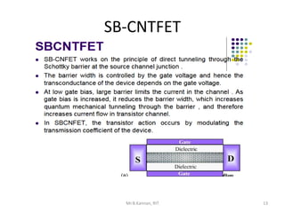
SB-CNTFET
Mr.B.Kannan, RIT 13
Mr.B.Kannan, RIT 14
Reference:
Yang, “Fundamentals of Semiconductor devices”, McGraw Hill International Edition,
1978.
Mr.B.Kannan, RIT 15

CNTFET

  • 1.
  • 2.
    CNTFET • CNT isa cylindrical shaped nanostructure, made of allotropes of carbon. • Bonding between the atom is very strong. • Diameter is in nano meter range. • Depending on the diameter of he nano tube,the intrinsic carrier concentration and bandgap will vary. Mr.B.Kannan, RIT 2
  • 3.
    • Advantage ofusing CNTFET • 1-D ballistic transport of electrons and holes • High drive current and large transconductance • High temperature resilience and strong covalent bond. Mr.B.Kannan, RIT 3
  • 4.
    • Single wallCNT is used as the channel between two electrodes which work as the source and drain contacts of a FET., a CNTFET can be fabricated. • Gate contacts wraps all around the channel (CNT), it has a very good control on carrier, and allows for better electrostatics. Mr.B.Kannan, RIT 4
  • 5.
  • 6.
    Types of carbonnano tubes. • Single walled carbon nanotube.(SWCNT) • Multi walled carbon Nanotube (MWCNT) Mr.B.Kannan, RIT 6
  • 7.
    CNTFET • 1998-first cntfetwas fabricated. • Nano scale device that has excellent mechanical and electrical properties. • Constrcution and opeartion is simlar to MOSFET. • In CNTFET-channel is formed by single semicondcuting CNT. • N-doped CNT is used as contact. • Pottassium doped source and drain regions are used to fabricate CNTFET. Mr.B.Kannan, RIT 7
  • 8.
  • 9.
    • Gate-control thecurrent across the source and drain terminal. • Gate-on-current flow in thew channel • MOSFET-channel made from lightly doped silicon. • CNTFET-channel is Carbon nano tubes. • P-type and N-type CNTFET.-unipolar device Mr.B.Kannan, RIT 9
  • 10.
    DC-characteristics(p-type and n-type) •Similar to MOSFET Mr.B.Kannan, RIT 10
  • 11.
    • Advantage andApplication. • Improved channel transport • Switching speed increases and device gets saturated faster. • Reduces power consumption,high gain and stable. • Implanted in logic circuits. • Operated in THz range.-high frequency regime. Mr.B.Kannan, RIT 11
  • 12.
    Types of CNTFET •MOS-CNTFET • SB-CNTFET Mr.B.Kannan, RIT 12
  • 13.
  • 14.
  • 15.
    Reference: Yang, “Fundamentals ofSemiconductor devices”, McGraw Hill International Edition, 1978. Mr.B.Kannan, RIT 15