Carbon nanotubes science and applications 1st Edition M. Meyyappan
Carbon nanotubes science and applications 1st Edition M. Meyyappan
Carbon nanotubes science and applications 1st Edition M. Meyyappan
Carbon nanotubes science and applications 1st Edition M. Meyyappan
Carbon nanotubes science and applications 1st Edition M. Meyyappan
1.
Visit https://ebookfinal.com todownload the full version and
explore more ebooks
Carbon nanotubes science and applications 1st
Edition M. Meyyappan
_____ Click the link below to download _____
https://ebookfinal.com/download/carbon-nanotubes-
science-and-applications-1st-edition-m-meyyappan/
Explore and download more ebooks at ebookfinal.com
2.
Here are somesuggested products you might be interested in.
Click the link to download
Carbon Nanotubes and Related Structures Synthesis
Characterization Functionalization and Applications 1st
Edition Guldi Dirk M. (Ed.)
https://ebookfinal.com/download/carbon-nanotubes-and-related-
structures-synthesis-characterization-functionalization-and-
applications-1st-edition-guldi-dirk-m-ed/
Carbon nanotubes properties and applications 1st Edition
O'Connell Michael J. (Ed.)
https://ebookfinal.com/download/carbon-nanotubes-properties-and-
applications-1st-edition-oconnell-michael-j-ed/
Carbon nanotubes and graphene 2nd Edition Kazuyoshi Tanaka
https://ebookfinal.com/download/carbon-nanotubes-and-graphene-2nd-
edition-kazuyoshi-tanaka/
Carbon nanotube science synthesis properties and
applications 1st Edition Harris Peter J.F.
https://ebookfinal.com/download/carbon-nanotube-science-synthesis-
properties-and-applications-1st-edition-harris-peter-j-f/
3.
Carbon Nanotubes TheoreticalConcepts and Research
Strategies for Engineers 1st Edition A. K. Haghi
https://ebookfinal.com/download/carbon-nanotubes-theoretical-concepts-
and-research-strategies-for-engineers-1st-edition-a-k-haghi/
One Dimensional Metals Conjugated Polymers Organic
Crystals Carbon Nanotubes 2nd Edition Siegmar Roth
https://ebookfinal.com/download/one-dimensional-metals-conjugated-
polymers-organic-crystals-carbon-nanotubes-2nd-edition-siegmar-roth/
Titanate and Titania Nanotubes Synthesis Properties and
Applications RSC Nanoscience and Nanotechnology 1st
Edition. Edition Dmitry V. Bavykin
https://ebookfinal.com/download/titanate-and-titania-nanotubes-
synthesis-properties-and-applications-rsc-nanoscience-and-
nanotechnology-1st-edition-edition-dmitry-v-bavykin/
Palladium Membrane Technology for Hydrogen Production
Carbon Capture and Other Applications Principles Energy
Production and Other Applications 1st Edition Doukelis
https://ebookfinal.com/download/palladium-membrane-technology-for-
hydrogen-production-carbon-capture-and-other-applications-principles-
energy-production-and-other-applications-1st-edition-doukelis/
Land Use and the Carbon Cycle Advances in Integrated
Science Management and Policy 1st Edition Daniel G. Brown
https://ebookfinal.com/download/land-use-and-the-carbon-cycle-
advances-in-integrated-science-management-and-policy-1st-edition-
daniel-g-brown/
5.
Carbon nanotubes scienceand applications 1st Edition M.
Meyyappan Digital Instant Download
Author(s): M. Meyyappan
ISBN(s): 9780849321115, 0849321115
Edition: 1
File Details: PDF, 15.06 MB
Year: 2005
Language: english
This ebook isfor the use of anyone anywhere in the United States
and most other parts of the world at no cost and with almost no
restrictions whatsoever. You may copy it, give it away or re-use it
under the terms of the Project Gutenberg License included with this
ebook or online at www.gutenberg.org. If you are not located in the
United States, you will have to check the laws of the country where
you are located before using this eBook.
Title: The Chevalier's daughter
or, An exile for the truth
Author: Lucy Ellen Guernsey
Release date: April 9, 2024 [eBook #73365]
Language: English
Original publication: London: John F. Shaw and Co, 1880
*** START OF THE PROJECT GUTENBERG EBOOK THE
CHEVALIER'S DAUGHTER ***
51.
Transcriber's note: Unusualand inconsistent spelling is
as printed.
We were soon safely hidden among the tall bushes and
wild vines, which covered the top of the rock, but not too soon,
for
52.
we were hardlysettled before the head of the procession
appeared in sight.
[The Stanton-Corbet Chronicles.]
[Year 1660]
THE
CHEVALIER'S DAUGHTER;
OR,
An Exile for the Truth.
BY
LUCY ELLEN GUERNSEY
AUTHOR OF
53.
LADY BETTY'S GOVERNESS,WINIFRED,
LADY ROSAMOND'S BOOK.
New Edition.
LONDON:
JOHN F. SHAW AND CO.
48 PATERNOSTER ROW, E.C.
STORIES BY L. E. GUERNSEY.
Large Crown 8vo, cloth, 5s.
OLDHAM; OR, BESIDE ALL WATERS.
The characters of the girls are capitally sketched—The
Christian.
The doctrinal teaching, warm, earnest, and devotional tone
of the story, are all we could desire.—Record.
Large Crown 8vo, cloth, 5s.
LOVEDAY'S HISTORY. A Story of Many Changes.
One of the most fascinating stories we have read.—Daily
Review.
A very interesting book, written in a very Christian and
charitable style.—Woman's Work.
54.
This delightful book.—Record.
Crown8vo, cloth, 5s.
THE FOSTER SISTERS. A Story of the Great Revival.
A pretty story of the last century; the style is bright and
sparkling.—Athenæum.
The story is charmingly told.—Guardian.
Crown 8vo, cloth, 5s.
THE CHEVALIER'S DAUGHTER; Or, An Exile for the Truth.
One of those quaint old world stories which the author
knows so well how to write.—Leeds Mercury.
Crown 8vo, cloth, 5s.
LADY BETTY'S GOVERNESS; Or, The Corbet Chronicles.
An unusually successful attempt to reproduce the manners of
the seventeenth century.—Saturday Review.
Crown 8vo, cloth, 5s.
LADY ROSAMOND'S BOOK; Or, Dawnings of Light.
A well-told story, written in quaint old-time style, the
plot interesting and well sustained, and the tone good.—Leeds
Mercury.
Crown 8vo, cloth, 3s. 6d.
WINIFRED. An English Maiden of the Seventeenth Century.
A truly delightful story, drawn to the life.—Leeds
Mercury.
LONDON: JOHN F. SHAW AND CO.
48, PATERNOSTER ROW, E.C.
55.
NOTE.
THESE memoirs werewritten by my
respected grandmother when she was quite an
old lady. I well remember as a child seeing her
writing upon them, my grandfather sitting near,
and she now and then suspending her pen to
talk over some incident with him. Matters have
not improved in France since her time, but 'tis
said that the young dauphin is quite a different
man from his father, and if he ever comes to
the throne, an effort will be made in behalf of
toleration for the persecuted Protestants. I hope
so, I am sure. But to return to the memoir.
After my grandparents' deaths, which took
place within a week of each other, the papers
were mislaid, and I only found them by accident
in an inner cupboard of a curious old carved
cabinet (I suspect the very one described in
these pages), which my younger brother took a
fancy to repair. I have amused the leisure
afforded me by a tedious sprained ankle in
arranging and transcribing these papers, which
seem to me both interesting and profitable.
ROSAMON
D GENEVIEVE CORBET.
56.
Tre Madoc Court,May 1st, 1740.
CONTENTS.
CHAPTER
I. Early Recollections
II. The Tour d'Antin
III. Youthful Days
IV. Trust and Distrust
V. Guests at the Tour
VI. The Lonely Grange
VII. A Sudden Summons
VIII. Flight
57.
IX. In Jersey
X.To England
XI. Tre Madoc
XII. Mischief
XIII. The Book
XIV. A Wedding
XV. Stanton Court
XVI. London
XVII. My New Friends
XVIII. A Great Step
XIX. Another Change
XX. You shall have no Choice
XXI. The Convent
XXII. The Voyage
XXIII. Conclusion
58.
THE CHEVALIER'S DAUGHTER
CHAPTERI.
EARLY RECOLLECTIONS.
I WAS born in the year of grace 1660, at the Tour
d'Antin, a château not very far from the little village of
Sartilly in Normandy.
My father was the Chevalier d'Antin, a younger son of
the Provençal family of De Fayrolles.
My mother was an English lady, daughter of a very
ancient Devonshire family. Her name was Margaret Corbet,
and the branch of that tribe to which she belonged had
settled in Cornwall. I remember her as a very beautiful
woman, with crispy waved blonde hair and a clear white
skin more like alabaster than marble, and no tinge of color
in her cheeks. I never saw any other person so pale as she,
though her lips were always red. She had beautiful gray
eyes, with long black lashes, and clearly defined arched
eyebrows meeting above her nose, which gave a very
serious and even solemn expression to her face. This
expression accorded well with her character, which was
grave and thoughtful and very deeply religious. I never saw
any person whose faith was so much like sight as hers.
Nevertheless, she could smile very sweetly, and even laugh
merrily at times, but not very often. For a shadow hung
59.
over our housefrom my earliest years—the same shadow
which darkened so many other French families at that time.
My father was a pleasant, lively, kindhearted
gentleman, who worshipped his beautiful wife, and treated
her as if she were indeed some fragile statue of alabaster
which might be broken by rough usage.
He was, as I have said, a younger son. His elder brother
lived far-away in Provence—at least his grand château was
there; but he and his wife spent most of their time at court,
where they both held offices about the king and queen. By
some family arrangement which I never understood, our
own Tour d'Antin came to my father, thus putting him in a
much more comfortable position than that of most younger
brothers, as there was a large and productive domain and
certain houses at Granville which brought good rents.
Besides, there were dues of fowls and so forth from the
tenants and small farmers. Indeed, my father, with his
simple country tastes, was far richer than his elder brother,
and that though my father's purse was always open to the
poor, especially those of our own household of faith.
The Tour d'Antin was a large building of reddish stone,
partly fortress, partly château. I suspect it had some time
been a convent also, for there was a paved court
surrounded by a cloister, and a small Gothic chapel which
was a good deal dilapidated, and never used in my time.
The fortress part of the house was very old. It consisted of
a square and a round tower, connected by a kind of gallery.
The walls were immensely thick, and so covered with
lichens and wall plants that one could hardly tell what they
were made of.
In the square tower my mother had her own private
apartment, consisting of a parlor and an anteroom, and an
60.
oratory, or closet,as we should call it in England, the last
being formed partly in the thickness of the wall, partly by a
projecting turret. It seemed an odd choice, as the new part
of the house was so light and cheerful, but there was a
reason for this choice which I came to understand
afterward.
The rooms communicated by a gallery with the newer
part of the house, where was a saloon, my father's special
study and business room, and various lodging rooms. This
same gallery, as I have said, led to the oldest part of the
château—the round tower, which was somewhat ruinous,
and where nobody lived but the bats and owls, and, if the
servants were to be credited, the ghosts of a certain
chevalier and his unhappy wife, about whom there was a
terribly tragical legend. There was a steep stone staircase
leading to the top of the round tower, from whence one
could see a very little bit of the sea and the great
monastery and fortress of St. Michael.
There was no view of the sea from any other part of the
house, which lay in a sort of dell or depression quite
sheltered from the winds, but from the hill behind us, one
could see the whole extent of the sands which lay between
Granville and the Mont St. Michel, and the mount itself, a
glorious vision in a clear bright day, and a gloomy sight
when it lowered huge and dark through the mists of
November.
We young ones used to look at it with sensations of
awe, for we knew that inside those high frowning walls,
shut deep from light and air, were horrible dungeons, in
which some of the Religion had perished in lingering
misery, and others might, for all we knew, be pining there
still. Formerly, we were told, the pinnacle of the fortress
61.
was crowned bya mighty gilded angel, an image of the
patron saint of the place, but it did not exist in my day.
The wide expanse of sand of which I have spoken was
and is called the Grève, and was no less an object of terror
to us than the fortress itself. It is a dreary and desolate
plain, abounding in shifting and fathomless quicksands,
which stretch on every hand and often change their places,
so that the most experienced guide cannot be sure of
safety. Not a year passes without many victims being
swallowed up by the Grève, and these accidents are
especially frequent about the time of the feast of St.
Michael, on the 29th of September, when crowds of pilgrims
flock to the mount from all over France. On the eve of All
Souls' Day—that is, on the 2d of November—as all good
Catholics in La Manche believe, there rises from the sands a
thick mist, and this mist is made up of the souls of those
unfortunates—pilgrims, fishermen, and smugglers—who
have from time to time found a horrible and living grave in
its treacherous depths, and who, having died without the
sacraments, are in at least a questionable position.
To the south and south-east of the Tour d'Antin lay wide
apple orchards, laden with fruit in good years, and seldom
failing altogether in bad ones. There was also a small
vineyard, but we made no wine, for Normandy is not a wine
country. The very children in arms drink cider as English
children drink milk, and it does not seem to hurt them. We
had a garden for herbs and vegetables—mostly salads,
carrots, and various kinds of pulse. Potatoes, which are
growing very common in England now, and were cultivated
to some extent even then, were unknown in France till long
afterward, and are not in use at present except as a rare
luxury.
62.
My mother hada flower-garden—very small, and
carefully tended by her own hands. At the end of our
garden stood a small unpretending stone building, not the
least like a church, which was nevertheless the only place of
worship of the Protestants for some miles around. For the
domain d'Antin was a kind of Protestant colony in the midst
of Catholics. All our own tenants were of the Religion, and
there were a few of the same way of thinking, both in
Granville and Sartilly, who came to the Temple, as it was
called, on the rare occasions when we had a visit from a
pastor.
On such occasions, we had sometimes as many as fifty
worshippers. When I recall the aspect of that little
congregation, with their solemn earnest faces, their blue
eyes fixed on the preacher, the old men and women with
their heads bent forward not to lose a word, the very
children in arms hushed and silent, and then look round on
our English congregation, with half the men asleep, the old
clerk nodding in his desk, or droning out the Amens, as my
naughty Walter says, like a dumbledore under a hat—when
I contrast the two, I sometimes wonder whether a little
persecution would not be good for the church on this side of
the water. It seems a poor way of praising the Lord for all
his benefits to go to sleep over them.
As I have said, the domain d'Antin was a kind of
Protestant colony in the midst of Roman Catholics—only we
did not use the word Protestant at that time. We were
among ourselves the Reformed, or the Religion; among
our enemies the Heretics, the religion pretended to be
reformed, and so forth. Our family had belonged to this
party ever since there had been any Reformed in France,
and even before.
63.
For our ancestorshad come into Provence from among
the Vaudois, of whom it was and is the boast that they had
never accepted the Romish corruptions of the true Gospel,
and therefore needed no reformation. For some hundreds of
years after their emigration, these people had lived in peace
with their neighbors. They had found Provence a wilderness,
all but abandoned to the wolves. They made it a smiling
garden. Vineyards and olive orchards, fruit and grain sprung
up where they trod. They were considered as odd people,
eccentric, perhaps a little mad, who would not swear nor
drink to excess, nor sing indecent songs, nor frequent
companies where such things were done; but then they
were quiet and peaceable, full of compassion for those who
needed help, paying dues to State and Church without a
murmur, and if they did not attend mass or confession, the
quiet old parish curés winked with both eyes, for the most
part, or contented themselves with mild admonitions to
such as came in their way.
But in the year 1540 all this was changed, and a
tempest fell on the peaceable inhabitants of Provence—a
tempest as unexpected by most of them as a thunderbolt
out of a clear sky. The preaching of the true Gospel, which
was begun about the year 1521 by Farel and Le Fevre,
spread like wildfire all over the kingdom. Crowds attended
everywhere on the ministrations of the reformed preachers,
and in many places, the parish priests were left to say mass
to the bare walls.
It seemed at first as if France would soon break away
from Rome, as Germany had done. But the fair dawn was
soon overclouded. Persecution arose because of the word,
and many were offended and returned to their former
observances.
64.
The Vaudois settlersin Provence were the greatest
sufferers. They were true to the faith of their forefathers,
and no menaces could shake them. Two of their villages—
Merindol and Cabrières—were burned to the ground. In the
former only one person was left alive—a poor idiot who had
given to a soldier two crowns for a ransom. The commander
of the expedition, d'Oppide, gave the soldier two crowns
from his own purse, and then caused the poor idiot to be
bound to a tree and shot. The men of Cabrières being
promised their lives and the lives of their families, laid down
their arms, and were cut in pieces on the spot. Women and
children were burned in their houses, others fled to the
mountains and woods to perish of want and cold, and the
name of Vaudois was almost extinguished in Provence. *
Almost, but not altogether.
* All these details and many more may be found in de
Félice's Histoire des Protestants de France, and in many
Catholic writers as well.
A hidden seed still remained among the poor and lowly,
and some great houses still openly professed their faith and
protected their immediate dependents. Among these was
the family to which my grandfather belonged. Through all
the troubles and wars of the League—through the fearful
days of St. Bartholomew, when France ran blood from one
end to the other—the family of my ancestors kept their
heads above the flood without ever denying their faith. It
remained for my uncle, the head of our family, to sully our
noble name by real or pretended conversion, in order to
curry court favor from Louis XIV. He has left no descendant
to perpetuate his shame. That branch of the family is
extinct, the last son being killed in a disgraceful duel.
65.
It was beforethis disgrace fell upon us that my father,
in consequence of the family arrangement I have spoken of,
took possession of the domain in Normandy. He was not a
very young man when, in a visit he made to Jersey, he met
and married my mother, who had also gone thither on a
visit.
We could see the island of Jersey on a clear day, like a
blue cloud on the horizon, and used to look at it with great
interest as a part of England, which we pictured to
ourselves as a land of all sorts of marvels.
From the time of the execution of the Edict of Nantes in
1598 to the death of Henry IV., those of the Religion in
France enjoyed a good degree of peace, and their temples
(which they were not allowed even then to call churches)
multiplied all over the land. But the Bearnois, as the people
loved to call him, was hardly cold in his grave before his
successor began his attempts to undo what his great
progenitor had done, and from that time to the final
revocation of our great charter in 1685, every year—nay,
almost every month—brought down new persecutions, new
edicts on the heads of the so-called Reformed. These
edicts were such as touched the honor, the safety, the very
life of every Protestant. I shall have to speak very largely of
these edicts as I proceed, for some of them had a direct
effect on my own destiny.
I have given a description of the Tour d'Antin as my
birthplace, but in truth my earliest recollections are of a
very different dwelling. For a long time after my birth, my
mother was in very delicate health and quite unable to
nurse me herself, so I was given over to the care of a
former servant of our family named Jeanne Sablot, who had
lately lost a young infant. Jeanne took me home to her own
house, and I only saw my dear mother at intervals of a
66.
month or twotill I was ten years old. Jeanne had two
children of her own, David and Lucille, both older than I,
and my sworn friends and protectors on all occasions.
Jeanne's parents had come from Provence, and she was like
an Italian, both in looks and ways. Her husband, Simon
Sablot, was a tall, blue-eyed, fair-haired Norman, somewhat
heavy and slow both in mind and ways, a devout Christian
man, respected even by his Roman Catholic neighbors for
his just dealings and generous hand.
But indeed we all lived in peace in those days. Catholics
and Protestants were neighborly together in the exchange
of good offices. Even the old curé did not hesitate to
exchange a kindly greeting with one of his heretical
parishioners, or to accept a seat and a drink of sparkling
cider in his dwelling. The great wave of persecution which
was sweeping over France had hardly reached our obscure
harbor, though we began to hear its roar at a distance.
The old farm-house in which my foster-parents lived
was roomy enough and very fairly neat, though the walls
and beams were black as ebony, and varnished with the
smoke of wood fires. I can see at this moment the row of
polished brass pans shining like gold in the firelight, the tall
drinking-glasses on the shelf, the oddly carved cabinet with
bright steel hinges, which Jeanne called a bahut, and
cherished with pride because it had come down from her
Vaudois ancestors, and the round brass jar used for milking,
and into whose narrow neck it required some skill to direct
the stream from the udder aright.
I can see my foster-father seated in his great chair in
the chimney corner, and my good nurse baking on the
griddle cakes of sarrasin, which the English call buckwheat.
These cakes were very good when they came hot and crisp
from the griddle; but it was and is the custom to bake up a
67.
Welcome to ourwebsite – the ideal destination for book lovers and
knowledge seekers. With a mission to inspire endlessly, we offer a
vast collection of books, ranging from classic literary works to
specialized publications, self-development books, and children's
literature. Each book is a new journey of discovery, expanding
knowledge and enriching the soul of the reade
Our website is not just a platform for buying books, but a bridge
connecting readers to the timeless values of culture and wisdom. With
an elegant, user-friendly interface and an intelligent search system,
we are committed to providing a quick and convenient shopping
experience. Additionally, our special promotions and home delivery
services ensure that you save time and fully enjoy the joy of reading.
Let us accompany you on the journey of exploring knowledge and
personal growth!
ebookfinal.com


![1
0-8493-2111-5/05/$0.00+$1.50
© 2005 by CRC Press LLC
1
Structures and
Properties of Carbon
Nanotubes
1.1 Bonding of Carbon Atoms....................................................2
1.2 Defect-Free Nanotube............................................................3
1.3 Defective Nanotubes ..............................................................6
1.4 Electronic Properties..............................................................8
1.5 Optical and Optoelectronic Properties...............................12
1.6 Mechanical and Electromechanical Properties ..................14
1.7 Magnetic and Electromagnetic Properties .........................17
1.8 Chemical and Electrochemical Properties..........................18
Wetting and Filling • Adsorption and Charge Transfer •
Chemical Doping, Intercalation, and Modification
1.9 Thermal and Thermoelectric Properties............................21
Since the discovery of carbon nanotubes (CNTs) by Iijima in 1991 [1], great progress has been made
toward many applications, including, for example:
• Materials
• Chemical and biological separation, purification, and catalysis
• Energy storage such as hydrogen storage, fuel cells, and the lithium battery
• Composites for coating, filling, and structural materials
• Devices
• Probes, sensors, and actuators for molecular imaging, sensing, and manipulation
• Transistors, memories, logic devices, and other nanoelectronic devices
• Field emission devices for x-ray instruments, flat panel display, and other vacuum nanoelec-
tronic applications
The advantages of these applications have been demonstrated, including their small size, low power,
low weight, and high performance, and will be discussed in the following chapters. These applications
and advantages can be understood by the unique structure and properties of nanotubes,as outlined below:
• Structures (Sections 1.1–1.3)
• Bonding: sp2 hybrid orbital allows carbon atoms to form hexagons and occasionally pentagons
and pentagon units by in-plane X bonding and out-of-plane U bonding.
• Defect-free nanotubes: these are tubular structures of hexagonal network with a diameter as
small as 0.4 nm. Tube curvature results in XU rehybridization or mixing.
Jie Han
NASA Ames Research Center
© 2005 by CRC Press LLC](https://image.slidesharecdn.com/81267-250225064130-f52b8093/75/Carbon-nanotubes-science-and-applications-1st-Edition-M-Meyyappan-15-2048.jpg)
![2 Carbon Nanotubes: Science and Applications
• Defective nanotubes: occasionally pentagons and heptagons are incorporated into a hexagonal
network to form bent, branched, coroidal, helical, or capped nanotubes.
• Properties (Sections 1.4–1.9)
• Electrical: electron confinement along the tube circumference makes a defect-free nanotube
either semiconducting or metallic with quantized conductance whereas pentagons and hepta-
gons will generate localized states.
• Optical and optoelectronic: direct band gap and one-dimensional band structure make nano-
tubes ideal for optical applications with wavelength ranging possibly from 300 to 3000 nm.
• Mechanical and electromechanical: XU rehybridization gives nanotubes the highest Young’s
modulus of over 1 TPa and tensile strength of over 100 GPa and remarkable electronic response
to strain and metal-insulator transition.
• Magnetic and electromagnetic: electron orbits circulating around a nanotube give rise to many
interesting phenomena such as quantum oscillation and metal-insulator transition.
• Chemical and electrochemical: high specific surface and XU rehybridization facilitate molecular
adsorption, doping, and charge transfer on nanotubes, which, in turn, modulates electronic
properties.
• Thermal and thermoelectric: inherited from graphite, nanotubes display the highest thermal
conductivity while the quantum effect shows up at low temperature.
1.1 Bonding of Carbon Atoms
To understand the structure and properties of nanotubes, the bonding structure and properties of carbon
atoms are discussed first. A carbon atom has six electrons with two of them filling the 1s orbital. The
remaining four electrons fill the sp3 or sp2 as well as the sp hybrid orbital, responsible for bonding
structures of diamond, graphite, nanotubes, or fullerenes, as shown in Figure 1.1.
In diamond [2], the four valence electrons of each carbon occupy the sp3 hybrid orbital and create
four equivalent X covalent bonds to connect four other carbons in the four tetrahedral directions. This
three-dimensional interlocking structure makes diamond the hardest known material. Because the elec-
trons in diamond form covalent X bonds and no delocalized U bonds, diamond is electrically insulating.
The electrons within diamond are tightly held within the bonds among the carbon atoms. These electrons
absorb light in the ultraviolet region but not in the visible or infrared region, so pure diamond appears
clear to human eyes. Diamond also has a high index of refraction, which makes large diamond single
crystals gems. Diamond has unusually high thermal conductivity.
In graphite [3], three outer-shell electrons of each carbon atom occupy the planar sp2 hybrid orbital
to form three in-plane X bonds with an out-of-plane U orbital (bond). This makes a planar hexagonal
network. van der Waals force holds sheets of hexagonal networks parallel with each other with a spacing
of 0.34 nm. The X bond is 0.14 nm long and 420 kcal/mol strong in sp2 orbital and is 0.15 nm and
360 kcal/mol in sp3 configuration. Therefore, graphite is stronger in-plane than diamond. In addition,
an out-of-plane U orbital or electron is distributed over a graphite plane and makes it more thermally
and electrically conductive. The interaction of the loose U electron with light causes graphite to appear
black. The weak van der Waals interaction among graphite sheets makes graphite soft and hence ideal
as a lubricant because the sheets are easy to glide relative to each other.
A CNT can be viewed as a hollow cylinder formed by rolling graphite sheets. Bonding in nanotubes
is essentially sp2. However, the circular curvature will cause quantum confinement and XU rehybridiza-
tion in which three Xbonds are slightly out of plane; for compensation, the U orbital is more delocalized
outside the tube. This makes nanotubes mechanically stronger, electrically and thermally more conduc-
tive, and chemically and biologically more active than graphite. In addition, they allow topological defects
such as pentagons and heptagons to be incorporated into the hexagonal network to form capped, bent,
toroidal, and helical nanotubes whereas electrons will be localized in pentagons and heptagons because
of redistribution of U electrons. For convention, we call a nanotube defect free if it is of only hexagonal
© 2005 by CRC Press LLC](https://image.slidesharecdn.com/81267-250225064130-f52b8093/75/Carbon-nanotubes-science-and-applications-1st-Edition-M-Meyyappan-16-2048.jpg)
![Structures and Properties of Carbon Nanotubes 3
network and defective if it also contains topological defects such as pentagon and heptagon or other
chemical and structural defects.
Fullerenes (C60) are made of 20 hexagons and 12 pentagons [4]. The bonding is also sp2, although
once again mixed with sp3 character because of high curvature. The special bonded structures in fullerene
molecules have provided several surprises such as metal–insulator transition, unusual magnetic correla-
tions, very rich electronic and optical band structures and properties, chemical functionalizations, and
molecular packing. Because of these properties, fullerenes have been widely exploited for electronic,
magnetic, optical, chemical, biological, and medical applications.
1.2 Defect-Free Nanotube
There has been a tremendous amount of work studying defect-free nanotubes, including single or
multiwalled nanotubes (SWNTs or MWNTs). A SWNT is a hollow cylinder of a graphite sheet whereas
a MWNT is a group of coaxial SWNTs. SWNT was discovered in 1993 [5,6], 2 years after the discovery
of MWNT [1]. They are often seen as straight or elastic bending structures individually or in ropes [7]
by transmission electron microscopy (TEM), scanning electron microscopy (SEM), atomic force micros-
copy (AFM), and scanning tunneling microscopy (STM). In addition, electron diffraction (EDR), x-ray
diffraction (XRD), Raman, and other optical spectroscopy can be also used to study structural features
of nanotubes. These characterization techniques will be discussed in detail in Chapter 5. Figure 1.2 shows
FIGURE 1.1 Bonding structures of diamond, graphite, nanotubes, and fullerenes: when a graphite sheet is rolled
over to form a nanotube, the sp2 hybrid orbital is deformed for rehybridization of sp2 toward sp3 orbital or XU bond
mixing. This rehybridization structural feature, together with electron confinement, gives nanotubes unique,
extraordinary electronic, mechanical, chemical, thermal, magnetic, and optical properties.
sp3
sp2
Deformed sp2
© 2005 by CRC Press LLC](https://image.slidesharecdn.com/81267-250225064130-f52b8093/75/Carbon-nanotubes-science-and-applications-1st-Edition-M-Meyyappan-17-2048.jpg)
![4 Carbon Nanotubes: Science and Applications
an STM image with atomic resolution of a single SWNT from which one can see the hexagonal structural
feature and TEM images of a SWNT rope and a few MWNTs.
A SWNT can be visualized as a hollow cylinder, formed by rolling over a graphite sheet. It can be
uniquely characterized by a vector C in terms of a set of two integers (n,m) corresponding to graphite
vectors a1 and a2 (Figure 1.3) [8],
C = na1+ ma2 (1.1)
Thus, the SWNT is constructed by rolling up the sheet such that the two end-points of the vector C
are superimposed. This tube is denoted as (n,m) tube with diameter given by
FIGURE 1.2 Homogeneous nanotubes of hexagonal network: TEM images (a), (b), and (c) for three multiwalled
nanotubes (MWNTs) first discovered by Iijima in 1991 [1]; TEM image (d) for a single-wall nanotube (SWNT) first
discovered by Iijima et al. in 1993 [5,6], an atomic resolution STM image (e) for a SWNT; and a TEM image (f) for
a SWNT rope first reported in 1996 by Thess et al. [7]. (Figures 1.2a and 1.2b are from Iijima, S., Nature, 354.56,
1991; Figure 1.2d is from Iijima, and Ichihashi, Nature, 363, 603, 1991; Figure 1.2f is from Thess et al., Science, 273,
483, 1996.)
FIGURE 1.3 A nanotube (n,m) is formed by rolling a graphite sheet along the chiral vector C = na1 + ma2 on the
graphite where a1 and a2 are graphite lattice vector. The nanotube can also be characterized by the diameter |C| and
the chiral angle V is with respect to the zigzag axis, V = 0°. The diagram is constructed for a (8,4) nanotube.
a b c
d e f
3 nm
armchair
T (8,4)
a2
zigzag
θ
a1
C
© 2005 by CRC Press LLC](https://image.slidesharecdn.com/81267-250225064130-f52b8093/75/Carbon-nanotubes-science-and-applications-1st-Edition-M-Meyyappan-18-2048.jpg)
![Structures and Properties of Carbon Nanotubes 5
D = |C|/U = a (n2 + nm + m2)1/2/U (1.2)
where a = |a1| = |a2| is lattice constant of graphite. The tubes with m = n are commonly referred to as
armchair tubes and m = 0 as zigzag tubes. Others are called chiral tubes in general with the chiral angle,
V, defined as that between the vector C and the zigzag direction a1,
V = tan–1 [31/2m/(m + 2n)] (1.3)
V ranges from 0 for zigzag (m = 0) and 30° for armchair (m = n) tubes. Note that is used for
convention.
The lattice constant and intertube spacing are required to generate a SWNT, SWNT bundle, and
MWNT. These two parameters vary with tube diameter or in radial direction. Most experimental mea-
surements and theoretical calculations agree that, on average, the C–C bond length dcc = 0.142 nm or
a = |a1| = |a2|= 0.246 nm and intertube spacing dtt, = 0.34 nm [8]. Thus, Equations (1.1) to (1.3) can
be used to model various tube structures and interpret experimental observations. Figure 1.4 illustrates
examples of nanotube models.
We now consider the energetics or stability of nanotubes. Strain energy caused by forming a SWNT
from a graphite sheet is proportional to 1/D per tube or 1/D2 per atom [9]. It is suggested [9–11] that
a SWNT should be at least 0.4 nm large to afford strain energy and at most about 3.0 nm large to maintain
tubular structure and prevent collapsing. Typical experimentally observed SWNT diameter is between
0.6 to 2.0 nm while smaller (0.4 nm) or larger (3.0 nm) SWNTs have been reported [12]. A larger SWNT
tends to collapse unless it is supported by other force or surrounded by neighboring tubes, for example,
as in a MWNT. The smallest innermost tube in a MWNT was found to be as small as 0.4 nm whereas
the outermost tube in a MWNT can be as large as hundreds of nm. But, typically, MWNT diameter is
larger than 2 nm inside and smaller than 100 nm outside. A SWNT rope is formed usually through a
self-organization process in which van der Waals force holds individual SWNTs together to form a triangle
lattice with lattice constant of 0.34 nm.
The structural model is of special interest to derive the tube chirality (n,m) from simple structural
relation or experimentally measurable geometry (D, V ). This is because important properties of a
nanotube are function of tube chirality, as will be discussed. For example, we may exclude the presence
of all zigzag tubes in a MWNT from the structural relations. The spacing between any two coaxial
neighboring zigzag tubes (n, 0) and (m, 0) is )D/2 = (0.123/U) (n-m) from Equation (1.2) and a = 0.246 nm.
FIGURE 1.4 By rolling a graphite sheet in different directions, two typical nanotubes can be obtained: zigzag (n,
0), armchair (m, m) and chiral (n,m) where nm0 by definition. In the specific example, they are (10,0), (6,6), and
(8,4) nanotubes.
(n,0)/ ZIG ZAG
(m, m)/ARM CHAIR
CHIRAL
(n, m)
n m
v
© 2005 by CRC Press LLC](https://image.slidesharecdn.com/81267-250225064130-f52b8093/75/Carbon-nanotubes-science-and-applications-1st-Edition-M-Meyyappan-19-2048.jpg)
![6 Carbon Nanotubes: Science and Applications
This, however, cannot be close to 0.34 nm spacing required to form a MWNT regardless of values of
integers n and m. However, a MWNT can be made of all armchair tubes (5 m, 5 m) where m = 1, 2, 3,
etc. The interspacing for all armchair MWNTs is )D/2 = (0.123/U)(3)1/2 (5) = 0.334 nm, very close to
0.34 nm. An experimentally observed MWNT can be interpreted with other models as well. For example,
a MWNT can also be viewed as a scrolled graphite sheet or a spiral graphite sheet, or mixture of scrolled
structure and concentric shells [13,14], rather than coaxial SWNTs. These models, however, have not
been accepted in general. But it is still likely that they present some of experimentally observed carbon
nanostructures or even reported MWNTs because graphite does show diverse structures such as graphite
whiskers and carbon fibers [3].
The significance of the tube chirality (n,m) is its direct relation with the electronic properties of a
nanotube. STM can be used to measure tube geometry (d, V), which, in turn, can be used to derive (n,m).
In the following sections, we will see a direct correlation of (n,m) with electronic, optical, magnetic, and
other properties of a nanotube.
1.3 Defective Nanotubes
In addition to defect-free nanotubes, experimentally observed structures also include the capped and
bent [15], branched (L, Y, and T) [16], and helical [17] MWNTs, and the bent [18], capped [19], and
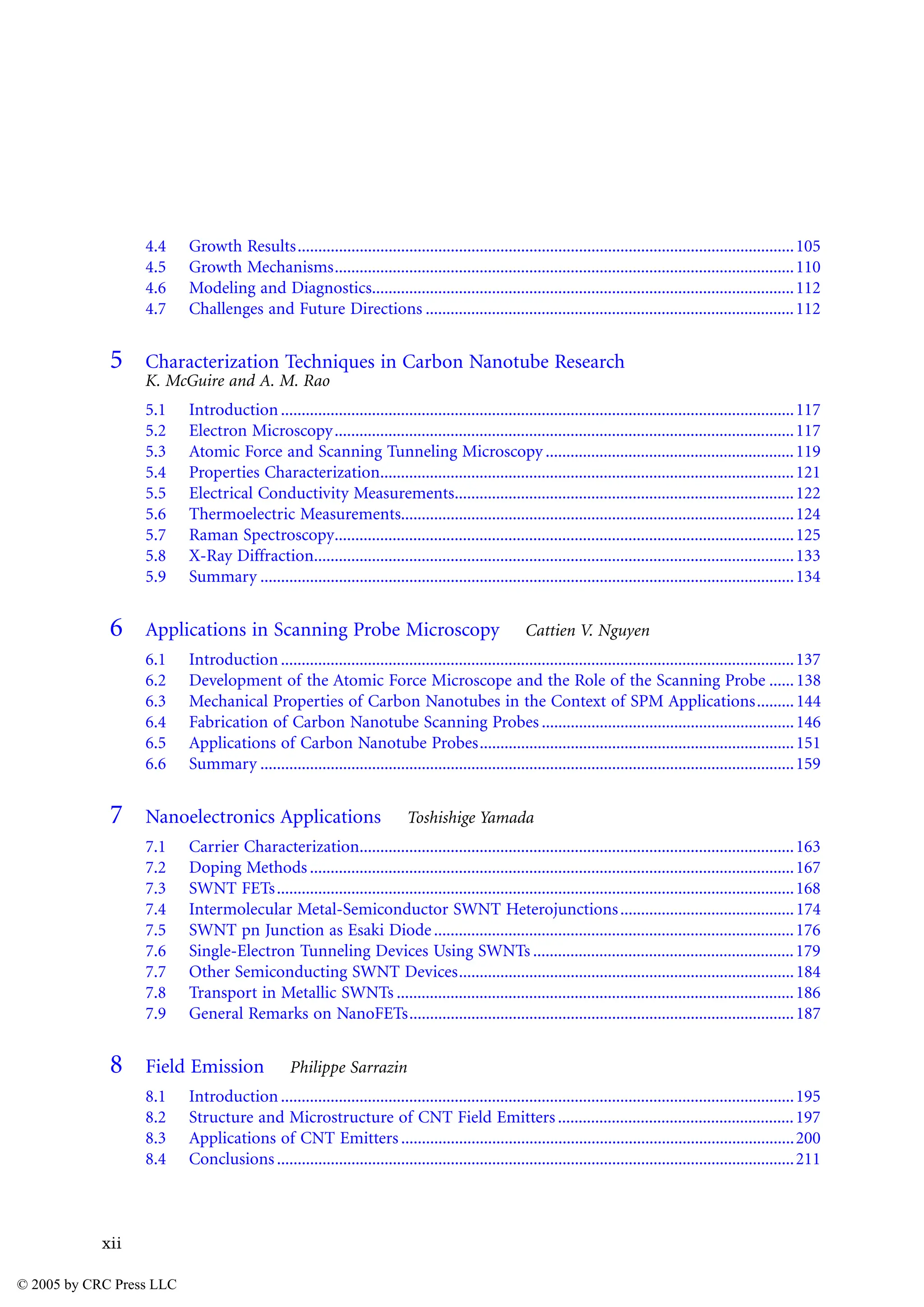
toroidal [20] SWNTs. Figure 1.5 shows TEM images of some of these structures. Most of these structures
are believed to have topological defects such as pentagons and heptagons incorporated in the nanotube
of hexagonal network. In addition, the reported MWNTs also include nontubular structures such as
multiwalled carbon nanofibers and bamboo structures, as illustrated in Figure 1.6. A bamboo structure
can be viewed as many capped short nanotubes. In general, most SWNTs are defect-free whereas MWNTs
are relatively more defective, containing either topological defects (pentagon-heptagon) or structural
defects (discontinuous or cone-shaped walls or bamboo structure).
Many approaches have been developed to model nanotubes containing topological defects because
these structures present intratube heterojunction nanoelectronic devices [21–24]. Han et al. have devel-
oped a generic approach and a computer program to generate and model configurations of bent [18],
branched [25,26], toroidal [27], and capped nanotubes [28]. In this approach, a single bend or each bend
in a branched, toroidal, or helical nanotube is considered to connect two types of nanotubes with the
topological defects (pentagon-heptagon pairs). The bend angle between two connected nanotubes follows
a simple topological relation [18]:
FIGURE 1.5 Representative TEM and AFM (insert) images of the individual SWNT bends. (a), (b) and (c) denote
three typical bend angles of 34°, 26°, and 18°[18], MWNT coils [17], and Y branches [16]. (Figure 1.5a from Zhang
et al., Appl. Phys. Lett., 83, 423, 2003; Figure 1.5c from Satishkumar et al., Appl. Phys. Lett., 77, 2530, 2000.)
a
b
c
a
300 nm
14 nm
50 nm
(b)
(a)
10 nm
© 2005 by CRC Press LLC](https://image.slidesharecdn.com/81267-250225064130-f52b8093/75/Carbon-nanotubes-science-and-applications-1st-Edition-M-Meyyappan-20-2048.jpg)
![8 Carbon Nanotubes: Science and Applications
of heptagons – number of pentagons) + 12]/6. Thus, to obtain 3- or 4-branched structure, the minimum
number of topological defects is 6 or 12 heptagons. In addition, any number of pentagon-heptagon pairs
is allowed, but this may cause extra energy.
In contrast, 6 or 12 pentagons are required to cap two or one end of a nanotube. For example, fullerenes
(C60) that contain 12 can be cut half to cap a (5,5) or (9,0) nanotube. However, for larger tubes, especially
for MWNTs, pentagon-heptagon pairs may be required to shrink a nanotube to a smaller size before
capping, as illustrated in Figure 1.6.
The current interest in nanotube junctions is largely from a theoretical point of view. Theoretically,
one can structure a variety of models to study their intriguing structures and properties. However,
experimentally all these structures are observed only occasionally.
In the following sections, we will mainly discuss the properties of defect-free nanotubes including (a)
an individual SWNT, (b) an individual MWNT, and sometimes (c) a SWNT rope. There has been a great
deal of work on defective, filmed, bundled, or arrayed SWNT or MWNT samples. However, the measured
properties, for example, in electrical and thermal conductivity and elastic modulus can vary by several
orders of magnitude from sample to sample. This is mainly because defective structures in a MWNT
and random orientation of various nanotubes in film or bulk samples have yet to be characterized or
specified and correlated with the properties of interest, which are mostly one-dimensional. These mea-
surements, however, are still of practical interest in applications and will be discussed in detail in the
following application chapters.
1.4 Electronic Properties
Electronic properties of nanotubes have received the greatest attention in nanotube research and applica-
tions. Extremely small size and the highly symmetric structure allow for remarkable quantum effects and
electronic, magnetic, and lattice properties of the nanotubes. Earlier theoretical calculations [29–31] and
FIGURE 1.7 Construction of a SWNT bend junction (10,0)-(6,6). (a) and (b), two graphite sheets representing
(10,0) and (6,6) nanotubes are connected to form a 30° planar bend; (b) and (c), the planar bend is rolled over to
form a 30° tube bend; and (c) and (d), the 30° bend is relaxed to a 36° bend via a molecular dynamics simulation.
The sj, mj, and I between four broken lines represent the unit cells of two tubes and junction interface [18].
A
B1 B
A
B2
(a) (b)
(d) (c)
C
sj
B1
B2
i
A
mj
θ
θo
θo
© 2005 by CRC Press LLC](https://image.slidesharecdn.com/81267-250225064130-f52b8093/75/Carbon-nanotubes-science-and-applications-1st-Edition-M-Meyyappan-22-2048.jpg)
![Structures and Properties of Carbon Nanotubes 9
later experimental measurements [32–37] have confirmed many extraordinary electronic properties, for
example, the quantum wire feature of a SWNT, SWNT bundle, and MWNT and the metallic and semi-
conducting characteristics of a SWNT.
In the simplest model [29–31], the electronic properties of a nanotube derived from the dispersion
relation of a graphite sheet with the wave vectors (kx, ky)
(1.6)
where L is the nearest neighbor-hopping parameter and a is lattice constant. L = 2.5 – 3.2 eV from different
sources [29–37] and a = 0.246 nm.
When the graphite is rolled over to form a nanotube, a periodic boundary condition is imposed along
the tube circumference or the C direction. This condition quantizes the two-dimensional wave vector
k = (kx, ky) along this direction. The k satisfying is allowed where q is an integer. This leads
to the following condition at which metallic conductance occurs:
(n – m) = 3q (1.7)
FIGURE 1.8 Examples of SWNT bend junctions. (a), a 34° bend has one pentagon and one heptagon in the opposite
sites of the joint; (b) to (d), a 26° bend has three pentagon-heptagon defects with one in opposite site and the other
two (fused) in different arrangements; (e), an 8° bend has two fused defects; and (f), a 4° bend has only one fused
defect [18].
p p
p
p
p
p
h
h
h
h
h
h
p
p
p
p
p
h
h
h
h
h
p
h
a. (10,10; 17,0; 34°) b. (11,9; 17,1; 25°)
c. (10,10; 16,2; 26°) d. (10,10; 16,2; 26°)
e. (10,10; 12,8; 8°) f. (10,10; 11,9; 4°)
E k k
k a k a k a
x y
x y y
( , ) { cos( )cos( ) cos ( )}
= ± + +
L 1 4
3
2 2
4
2
2 1 2
k š =
C q
2U
© 2005 by CRC Press LLC](https://image.slidesharecdn.com/81267-250225064130-f52b8093/75/Carbon-nanotubes-science-and-applications-1st-Edition-M-Meyyappan-23-2048.jpg)
![10 Carbon Nanotubes: Science and Applications
This suggests that one third of the tubes are metallic and two thirds are semiconducting. The band
gap for a semiconducting tube is give by
Eg = 2dccL/D (1.8)
Thus, the band gap of a 1-nm wide semiconducting tube is roughly 0.70 eV to 0.9 eV. This relation
is in good agreement with STM experimental measurement for single SWNTs [35,36]. The STM mea-
surements also confirm the density of state (DOS) or band structure predicted from the dispersion
relation of graphite imposed with tubular periodic boundary condition. The DOS of SWNT will be
discussed in the following section.
The derivation from graphite does not consider the curvature effect or XU rehybridization. This effect
has been investigated using various approaches, including first principle ab-initio calculations [38–42,65].
It is found that XU rehybridization can open up a small band gap (~0.02 eV) for smaller (1.5 nm)
nonarmchair metallic tubes, as can be seen from Figure 1.13. A STM study indeed confirms such a small
gap for n – m = 3q SWNT [41]. However, this effect is found to be very rapidly disappearing with the
tube diameter. In principle, only armchair tubes are intrinsically metallic. However, for most discussions
the metallic condition (n-m) = 3q and the band gap and structures predicted from only the simplest
U-orbital model have been accepted.
Intertube coupling needs to be considered when the results of a SWNT are used for a SNWT rope or
a MWNT. Calculations reveal interesting intertube coupling properties. The intertube coupling induces
a small band gap for certain metallic tubes [42] but a reduced band gap by 40% for semiconducting
tubes [43] in a SWNT rope. Similar observations can be expected for a MWNT as well, but the intertube
coupling is relatively smaller because of bigger diameter in a MWNT. For example, it is predicted that
two metallic tubes (5,5) and (10,10) in a coaxial MWNT can both open a small bang gap [43], but (10,10)
and (15,15) tubes in a MWNT are found to remain metallic because of less intertube coupling for larger
tubes.All semiconducting tubes in a MWNT tend to be semi-metallic just like graphite because of reduced
band gap for large tubes and hole-electron pairing for multiwall coupling. More experiments on indi-
vidual MWNT samples indeed show the dominating metallic or semimetallic nature of a MWNT while
small band gap was reported and attributed to presence of defects or an electric contact barrier.
It has been experimentally confirmed that a single SWNT [32], a SWNT rope [33], or a MWNT [34]
behave like a quantum wire intrinsically because of the confinement effect on the tube circumference. A
FIGURE 1.9 UV-VIS-NIR spectra from different SWNT sample types. (a) Spectrum of SWNT rope material shown
for comparison together with the spectrum of colloidal graphite (offset for clarity). (b) A, B, and C features can be
attributed to symmetric transitions between the lowest subbands in semiconducting (A, B) and metallic (C) tubes
in representative density of states (DOS). (From A. Hagen and T. Hertel, Nano Lett., 3, 383, 2003.)
Optical
density
(arb.units)
Density
of
states
1.0 2.0 3.0
Photon energy (eV)
SWNT (PLV)
A B C
colloidal graphite
(a) (b)
B
A
C
semi-
conducting
metallic
4.0 −1 0
Energy (eV)
1
© 2005 by CRC Press LLC](https://image.slidesharecdn.com/81267-250225064130-f52b8093/75/Carbon-nanotubes-science-and-applications-1st-Edition-M-Meyyappan-24-2048.jpg)
![Structures and Properties of Carbon Nanotubes 11
MWNT or a SWNT rope can be viewed as a parallel assembly of single SWNTs. The conductance for a
SWNT, a SWNT rope, or MWNT is given by
G = Go M = (2e2/h) M (1.9)
where Go = (2e2/h) = (12.9 k)–1 is quantized conductance. M is an apparent number of conducting
channels including electron-electron coupling and intertube coupling effects in addition to intrinsic
channels. M = 2 for a perfect SWMT. M, however, is determined not only by the intrinsic properties of
a nanotube itself, but also by the intertube coupling as discussed above and the scatters such as defects,
impurities, structural distortions, coupling with substrate, and contacts. Therefore, the experimentally
measured conductance is much lower than the quantized value. The measured resistance for a single
SWNT is ~10 k [44], as compared with the perfect value of 12.9/2 or 6.45 k.
Transport properties of nanotubes and physics of the devices fabricated using these structures will be
discussed in Chapter 7. Here a brief discussion is made to compare the resistivity or conductivity of
graphite and nanotubes. There have been a number of reports on the measured resistance of nanotubes,
but most of them cannot be compared or cited here because the reported resistance, not resistivity, lacked
the specification for the sample quality and measurement conditions and other details. The resistivity of
graphite varies remarkably depending on sample quality. As temperature increases, it can decrease for
disordered structures or increase for highly ordered structures such as a single crystal. The room tem-
perature in-plane resistivity of the highest quality graphite is about 0.4 µm [3]. In many measurements
of SWNT ropes and MWNTs, the resistivity is found to decrease with temperature, and the room
temperature values are much higher than 0.4 µm. This is mainly because nanotubes are randomly
oriented in the sample. When the measurement is carried out for the purified SWNT ropes or MWNTs
aligned across four electrodes, the result is consistently comparable with or lower than 0.4 µm [44,45].
The U electron is more delocalized in a defect-free nanotube because of XU rehybridization and thus
should give rise to higher conductivity than that of graphite. As shown in Figure 1.1, when curved, U
orbitals become rich or more delocalized outside the tube, which leads to increased conductivity. Many
measurements show decreasing behavior of resistivity with temperature. This, however, is not due to
semiconducting nanotubes but the contact, intertube coupling, defects, tube alignment, or other issues
[44]. The nanotube is a one-dimensional conductor and has to be aligned between two electrodes for
transport measurement.
More theoretical attention has been paid to the electronic properties of heterogeneous nanotubes,
especially bent and branched structures. There are three main features for these structures [18,21–25,
46,47]. First, these structures are molecular mimics of 2- or 3-terminal heterojunctions that connect two
or three different nanotubes in the form of A-B or A-B-C in which A, B, or C can be a metallic or
semiconducting tube. Second, localized states appear in the junction interface containing pentagons and
heptagons. Out of this region, each tube retains its own band structure or density of state. Third, the
interface may or may not be conducting, depending on how tubes are connected. For example, a (9,0)-
(6,3) tube junction is not conducting for symmetric match but conducting for asymmetric match. The
symmetric match retains straight tube geometry, which is difficult to be observed experimentally. Asym-
metric match leads to a bend structure. Experimental observations indeed confirmed theoretical predic-
tions for SWNT bent junctions [18,36]. MWNT heterojunctions are observed more frequently. However,
there has not been any controlled way to experimentally fabricate them especially from SWNTs.
Localized states are originated from pentagons and heptagons incorporated in a hexagonal network.
They are also observed in capped SWNT and MWNT ends. These localized states are responsible for
enhanced field emission and interface states at nanotube junctions.
The novel electronic properties of nanotubes have attracted great interest in applications of nanotubes
in nanoelectronics. Much of the effort to date has been made in using individual semiconductor SWNTs
for transistors, memories, and logic devices. The striking feature of these nanoelectronic devices is higher
mobility and stronger field effect. In addition, nanotube junctions such as sharp bends and T and Y
branches have been studied as nanoelectronics devices [48,49]. Furthermore, the electronic properties
© 2005 by CRC Press LLC](https://image.slidesharecdn.com/81267-250225064130-f52b8093/75/Carbon-nanotubes-science-and-applications-1st-Edition-M-Meyyappan-25-2048.jpg)
![12 Carbon Nanotubes: Science and Applications
have been correlated with mechanical, chemical, biological, thermal, and magnetic interactions with
nanotubes. As a result, the extended electromechanical, electrochemical, thermal electronic, and electro-
magnetic properties are associated with applications of CNTs in sensors, actuators, field emission, bat-
teries, fuel cells, capacitors, and many others.
1.5 Optical and Optoelectronic Properties
Defect-free nanotubes, especially SWNTs, offer direct band gap and well-defined band and subband
structure, which is ideal for optical and optoelectronic applications. Optical spectra have been estab-
lished for individual SWNTs and ropes using resonant Raman [50], fluorescence [51–53], and ultraviolet
to the near infrared (UV-VIS-NIR) spectroscopies [54]. In addition, electrically induced optical emis-
sion [55] and photoconductivity [56] have been studied for individual SNWTs. A typical optical
spectrum measured for a SWNT rope is shown in Figure 1.10 with that for a graphite sample for
comparison [54]. Three peaks for the SWNT ropes cannot be observed for the graphite and attributed
to symmetric transitions between the lowest subbands in semiconducting (A and B) and metallic (C)
tubes. Usually, as-grown nanotube samples are a mixture of semiconducting and metallic tubes, as
mentioned before. The measured peak position and intensity are correlated with electronic structures
or tube chiralty (n,m) or (D,V). Therefore, optical spectra have been extensively used to determine the
detailed composition of SWNT samples. This will be further detailed in Chapter 5. Here we discuss
only the fundamental optical and optoelectronic properties of nanotubes.
Optical and optoelectronic properties can be understood from the band structure or DOS of a SWNT.
The one-dimensional DOS of a SWNT can be derived from that for graphite with the expression as
follows:
(1.10)
FIGURE 1.10 Calculated electronic DOS of metallic (10,10) and (11,8) and semiconducting (12,7) tubes using
tight-binding calculations with the Fermi level positioned at zero energy.
Density
of
States
2.0
1.0
0.0
Energy (eV)
−1.0
−2.0
(10,10)
(11,8)
(12,7)
W J
L
J J
( ) ( , )
=
=h
h
¨
4 2
3
l a
g m
m
© 2005 by CRC Press LLC](https://image.slidesharecdn.com/81267-250225064130-f52b8093/75/Carbon-nanotubes-science-and-applications-1st-Edition-M-Meyyappan-26-2048.jpg)
![Structures and Properties of Carbon Nanotubes 13
where
for
for
As an example, Figure 1.10 shows calculated electronic DOS of metallic (10,10), (11,8) and semicon-
ducting (12,7) tubes. The Fermi level is positioned to zero. The left and right side to the Fermi level
define valence and conductance band, respectively. The peak of DOS is called van Hove singularity (VHS).
The optical transition occurs when electrons or holes are excited from one energy level to another,denoted
by Epq. The selection rules, p-q = 0, for interband transitions that are symmetric with respect to the Fermi
level require polarized light parallel to the tube axis, as shown by A, B, and C absorption features of
Figure 1.9. The other selection rules that require perpendicular light to tube axis, however, have not been
observed in optical spectra probably because of too-weak transitions. The energy corresponding to the
symmetric transition p = q for semiconducting (S) and metallic tubes (M) follows the relations with one
p-orbital approximation:
Epp,S = 2pdccL/D and Epp,M = 6pdccL/D (1.11)
The number p (p = 1, 2…) is used to denote the order of the valence and conduction bands symmet-
rically located with respect to the Fermi energy. Note that p = 1 defines the band gap of a semiconducting
tube. Thus, a map can be made taking possible values of p and D for metallic and semiconducting tubes,
as shown in Figure 1.12.
Figure 1.11 includes tube curvature-induced s-p rehybridization effect with which only armchair tubes
(n=m) are truly metallic whereas others satisfying n-m = 3q are semi-metallic with small band gap. The
energy unit in Figure 1.11 is L eV. Taking L = 2.5 (low bound) and 3.0 eV (high bound), the wavelength
of a semiconducting tube (= hc/E) can vary from 300 to 3000 nm. This suggests potential applications
of semiconducting nanotubes in optical and optoelectronic devices from blue lasers to IR detectors.
For example, IR laser-excited photoconductivity was observed for a semiconducting SWNT within an
ambipolar field effect transistor device [56]. This suggests that a semiconducting SWNT can be used for
a polarized IR photo detector in which the photocurrent is nearly a linear function of IR intensity. In
contrast, the same device can be also used for optoelectronic devices such as a light emitter in which
emission of wavelength of 1500 nm is induced electronically [55]. Unlike conventional solid state opto-
electronics, the semiconducting SWNT can emit light from injecting electrons and holes from two contact
electrodes, instead of doping. Electrical control of the light emission of individual SWNTs allows detailed
characterization of the optical properties. Another experiment is the observation of light emission by
injecting electrons through a STM into MWNTs. The emitted photon wavelength is in the range of 600
to 1000 nm [57]. However, the emission is associated with localized states in the nanotube tips. In addition
to STM ejection of electrons,light emission was also observed when coupled with electron (field) emission
[58].A peak was clearly seen close to 1.8 eV.Again,this is attributed to localized states at the nanotube tips.
It is still very challenging to study the optical and optoelectronic properties of a single nanotube.
Extensive work has been carried out to establish the structure-assigned optical spectra for identification
of Raman-active, infrared-active photon modes from samples containing different diameters and chiral-
ities of nanotubes. In principle, the assignment can be readily established based on the unique VHSs in
the electronic density of states. For example, one can assign tube chirality (n,m) from the measured
photonic energy and image-measured diameter using Figure 1.12. Simulation and experimental studies
g m m
( , )
J J J J J
=
2 2
J J
m
g m
( , )
J J = 0 J J
m
J
L
m
q n m a
D
=
+
3
3
© 2005 by CRC Press LLC](https://image.slidesharecdn.com/81267-250225064130-f52b8093/75/Carbon-nanotubes-science-and-applications-1st-Edition-M-Meyyappan-27-2048.jpg)
![14 Carbon Nanotubes: Science and Applications
have found much different absorption coefficient spectra for nanotubes and strong dependence of
nonlinear optical properties on the diameter and symmetry of the tubes [51–55]. One can expect that
these dependences become more complicated for MWNTs. In addition, the electronic and optical prop-
erties of nanotubes are strongly coupled with mechanical, chemical (environmental), thermal, and
magnetic (radiation etc.) properties, as will be discussed in the following sections. This will further
complicate characterization of the nanotube structure and properties.
1.6 Mechanical and Electromechanical Properties
X bonding is the strongest in nature, and thus a nanotube that is structured with all X bonding is regarded
as the ultimate fiber with the strength in its tube axis. Both experimental measurements and theoretical
calculations agree that a nanotube is as stiff as or stiffer than diamond with the highest Young’s modulus
and tensile strength. Most theoretical calculations are carried out for perfect structures and give very
consistent results [27,59,60].Table 1.1 summarizes calculatedYoung’s modulus (tube axis elastic constant)
and tensile strength for (10,10) SWNT and bundle and MWNT with comparison with other materials.
The calculation is in agreement with experiments on average [61–64]. Experimental results show broad
discrepancy, especially for MWNTs, because MWNTs contain different amount of defects from different
growth approaches.
In general, various types of defect-free nanotubes are stronger than graphite. This is mainly because
the axial component of X bonding is greatly increased when a graphite sheet is rolled over to form a
seamless cylinderical structure or a SWNT. Young’s modulus is independent of tube chirality, but depen-
dent on tube diameter. The highest value is from tube diameter between 1 and 2 nm, about 1 TPa. Large
tube is approaching graphite and smaller one is less mechanically stable. When different diameters of
SWNTs consist in a coaxial MWNT, the Young’s modulus will take the highest value of a SWNT plus
contributions from coaxial intertube coupling or van der Waals force. Thus, the Young’s modulus for
MWNT is higher than a SWNT, typically 1.1 to 1.3 TPa, as determined both experimentally and
FIGURE 1.11 Energies for symmetric interband transitions in SWNTs as a function of their diameter. (From A.
Hagen and T. Hertel, Nano Lett., 3, 383, 2003.)
Gap
energy
(γ
0
) 0.8
a)
0.6
0.4
0.2
0.0
4 8
semiconducting
small gap semiconducting
metallic
12
Diameter (Å)
16
1.0
ε22
M
ε44
S
ε33
S
ε11
M
ε22
S
ε11
S
ε00
M
© 2005 by CRC Press LLC](https://image.slidesharecdn.com/81267-250225064130-f52b8093/75/Carbon-nanotubes-science-and-applications-1st-Edition-M-Meyyappan-28-2048.jpg)
![Structures and Properties of Carbon Nanotubes 15
FIGURE 1.12 Band gap change of SWNTs under uniaxial strain (0 for tension and 0 for compression) and
torsional strain (0) for net bond stretching and 0 for net bond compression), predicted by Equation (1.10) [65].
TABLE 1.1 Mechanical Properties of Nanotubes
Young’s modulus
(GPa)
Tensile Strength
(GPa)
Density
(g/cm3)
MWNT
SWNT
SWNT bundle
Graphite (in-plane)
Steel
1200
1054
563
350
208
~150
75
~150
2.5
0.4
2.6
1.3
1.3
2.6
7.8
Source: J. Lu and J. Han, Int. J. High Speed Electron. Sys. 9, 101 (1998). With permission.
∆E
gap
/(3t
o
)/(1
+
ν)
×
10
2
)
−1.0
−0.5
0.0
0.5
1.0
∆E
gap
/(3t
o
)
(×
10
2
)
−1.0
−1.0 −0.5 0.0
Strain
0.5 1.0
(15,5)
(8,1)
(19,0)
(16,2)
(21,7)
(10,10)
(17,0)
(16,8)
(8,6)
(10,10)
(16,12)
(14,7)
uniaxial
torsional
(19,0)
−0.5
0.0
0.5
1.0
© 2005 by CRC Press LLC](https://image.slidesharecdn.com/81267-250225064130-f52b8093/75/Carbon-nanotubes-science-and-applications-1st-Edition-M-Meyyappan-29-2048.jpg)
![16 Carbon Nanotubes: Science and Applications
theoretically. On the other hand, when many SWNTs are held together in a bundle or a rope, the weak
van der Waal force induces a strong shearing among the packed SWNTs. This does not increase but
decreases the Young’s modulus. It is shown experimentally that the Young’s modulus decreases from
1 TPa to 100 GPa when the diameter of a SWNT bundle increases from 3 nm (about 7 (10,10) SWNTs)
to 20 nm [64].
The elastic response of a nanotube to deformation is also very remarkable. Most hard materials fail
with a strain of 1% or less due to propagation of dislocations and defects. Both theory and experiment
show that CNTs can sustain up to 15% tensile strain before fracture [27]. Thus the tensile strength of
individual nanotube can be as high as 150 GPa, assuming 1 TPa for Young’s modulus. Such a high strain
is attributed to an elastic buckling through which high stress is released. Elastic buckling also exists in
twisting and bending deformation of nanotubes. All elastic deformation including tensile (stretching and
compression), twisting, and bending in a nanotube is nonlinear, featured by elastic buckling up to ~15%
or even higher strain. This is another unique property of nanotubes, and such a high elastic strain for
several deformation modes is originated from sp2 rehybridization in nanotubes through which the high
strain gets released.
However, sp2 rehybridization will lead to change in electronic properties of a nanotube. A position
vector in a deformed nanotube or graphite sheet can be written as r = ro + )r where r can be deformed
lattice vector a or chiral vector C described in Section 1.4. Using a similar approach to deriving electronic
properties of a nanotube from graphite, the following relations are obtained [65]:
Eg = Ego + sgn (2 p + 1) 3L [(1 + Z) (cos 3V) Jl + (sin 3V) Jr ] (1.12)
In this relation, Ego is zero strain band gap given by Equation (1.6); V is nanotube chiral angle defined
by Equation (1.3); Jl and Jr are tensile and torsion strain, respectively; and Zis Poisson’s ratio. Parameter
p is defined by (n – m) = 3q + p such that p = 0 for metallic tube; p = 1 for type I semiconductor
tube, for example, (10,0); and p = –1 for type II semiconductor tube, for example, (8,0). Thus, function
sgn(2p +1) = 1, 1 and –1, respectively, for these three types of tubes. Equation (1.12) predicts that all
chiral or asymmetric tubes (0 V 30°) will experience change in electronic properties for either tensile
or torsional strain whereas symmetric armchair or zigzag tubes may or may not change their electronic
properties. In asymmetric tubes, either strain will cause asymmetric XU rehybridization and therefore
change in electronic properties. However, effect of strain on a symmetric tube is not so straightforward.
A detailed explanation is given in the original publications together with analysis of DOS. Figure 1.12
shows band gap change for different nanotubes.
The most interesting is the predicted metal-insulator transition. The armchair tube is intrinsically
metallic but will open a band gap under torsional strain. The zigzag (3q, 0) metallic tube, instead, will
open a band gap under tensile strain, not torsional strain. The chiral metallic tube, for example, (9,3),
will open band gap in either case. The above theory can also be extended to tube bending. For pure
bending where bond stretching and compression cancel each other along tube circumference without
torsion deformation, the band gap should not change from that predicted from Equation (1.12). However,
there are exceptions. For example, when a SWNT with two ends fixed by two electrode leads is subject
to a bending deformation applied by an AFM tip, the deformation also generates a net tensile stretching
strain. Metal-insulator (semiconductor) transition and a decrease in conductance with strain are indeed
observed experimentally in this case. Experiments have confirmed the predicted remarkable electro-
mechanical properties of nanotubes or electronic response to mechanical deformation [66,67].
Equation (1.12) does not include sp2 hybridization effect. Again, the effect is found very small, similar
to that for the tube under no deformation, as shown in Figure 1.3. Figure 1.3 shows striking features of
electromechanical properties of a nanotube such as splitting and merging of VHS peaks including band
gap opening and closing under mechanical deformation.
There has not been much effort studying the electromechanical properties of SWNT bundles and
MWNTs. Intertube coupling may play a larger role in electromechanical properties as it does for Young’s
modulus and tensile strength.
© 2005 by CRC Press LLC](https://image.slidesharecdn.com/81267-250225064130-f52b8093/75/Carbon-nanotubes-science-and-applications-1st-Edition-M-Meyyappan-30-2048.jpg)
![Structures and Properties of Carbon Nanotubes 17
1.7 Magnetic and Electromagnetic Properties
Similar to mechanical and electromechanical properties, magnetic and electromagnetic properties of
CNTs are also of great interest. The magnetic properties are studied with electron spin resonance (ESR),
which is very important in understanding electronic properties, for example, for graphite and conjugated
materials. Once again, there is a large discrepancy from different experimental measurements, especially
FIGURE 1.13 DOS with (dash line) and without (solid line) consideration of s-p rehybridization for three typical
SWNTS. Values on the right side are stains. A small band gap of 0.02 eV at zero strain, caused by tube curvature or
rehybridization, is seen for tube (18,0). Striking features of electromechanical properties include splitting and merging
of VHS peaks including band gap opening and closing [65].
DOS
(arb.)
3
2
1
0
3.2%
4%
0%
1%
3%
4%
0%
1%
3%
4%
1%
−1.5 −1.0 −0.5 0.0
E (ev)
0.5 1.0 1.5
0%
(a) (17, 0), p = −1
(b) (18, 0), p = 0
(c) (19, 0), p = +1
© 2005 by CRC Press LLC](https://image.slidesharecdn.com/81267-250225064130-f52b8093/75/Carbon-nanotubes-science-and-applications-1st-Edition-M-Meyyappan-31-2048.jpg)
![18 Carbon Nanotubes: Science and Applications
in transport properties, because of sample quality and alignment whereas qualitatively they agree with
theoretical calculations.
Magnetic properties such as anisotropic g-factor and susceptibility of nanotubes are expected to be
similar to those for graphite while some unusual properties may exist for nanotubes. Indeed, it is found
from ESR [68] that the average observed g-value of 2.012 and spin susceptibility of 7×10⁻⁹ emu/g in
MWNTs are only slightly lower than 2.018 and 2×10⁻⁸ emu/g in graphite. Some interesting properties
are also found from ESR studies of Pauli behavior. For example, aligned MWNTs are metallic or semi-
metallic. The measured susceptibility gives the density of state at the Fermi level of 1.5×10⁻³ states/eV/
atom, also comparable with that for in-plane graphite. The carrier concentration is about 1019cm–3, as
compared with an upper limit of 1019 cm–3 from Hall measurement. However, similar observations have
not been made for SWNTs and bundles. The possible reason is sample alignment difficulties and strong
electron correlation, which may block nonconduction ESR signal.
It can also be expected that CNTs would have interesting electrical response to a magnetic field. Indeed,
both experiment and theory confirm the metal-insulator transition and band gap change whereas trans-
port again is an intriguing issue. A similar approach to those in previous sections can be adopted to
predict Landau band structure of nanotubes in magnetic field. However, the hopping parameter in
Equation (1.5) will be multiplied by magnetic flux, K=(h/e)(G/3)orG=3K/(h/e) where (h/e) is the magnetic
flux quantum. Thus, the band gap of nanotube under uniform magnetic filed parallel to the tube axis is
given by [69]:
For metallic tubes of n – m = 3q
*g = *gT G, 0 G 3/2
*g = *gT |3 – G|, 3/2 G 3
For semiconducting tubes
*g = *go |1 – G|, 0 G 3/2
*g = *gT |2 – G|, 3/2 G 3
These relations predict a metal-insulator transition and band gap change for semiconductor tubes
under magnetic field parallel to tube axis. This is similar to electrical response of nanotubes to mechanical
deformation. Qualitatively the electronic response of three types of nanotubes under either magnetic
field or strain field parallel tube axis can be schematically shown in Figure 1.15. Driven by magnetic or
strain field, the Fermi level will move away from the original position, and this results in the band gap
change pattern in Figure 1.15. This is explained in Figure 1.14 and quantified in Yang and Han [65].
Similar response can also be observed when magnetic field or strain field is perpendicular to tube axis.
A major feature from the theory is that the band gap change is oscillatory and that the semiconducting
and metallic nature of nanotubes can be altered by applying a magnetic field or strain field. This is called
Aharonov-Bohm effect in magnetic field case. The oscillatory behavior is confirmed by experimental
measurements of resistance change in MWNTs with tube axis parallel to magnetic field [70]. In the
experiments, only the outermost tube in the MWNT is considered to contact with electrode leads and
to contribute to the measured resistance.
1.8 Chemical and Electrochemical Properties
Small radius, large specific surfaces and XU rehybridization make CNTs very attractive in chemical and
biological applications because of their strong sensitivity to chemical or environmental interactions.
These, however, also present challenges in characterization and understanding of other properties. The
chemical properties of interest include opening, wetting, filling, adsorption, charge transfer, doping,
intercalation, etc. Applications include chemical and biological separation, purification, sensing and
detection, energy storage, and electronics.
© 2005 by CRC Press LLC](https://image.slidesharecdn.com/81267-250225064130-f52b8093/75/Carbon-nanotubes-science-and-applications-1st-Edition-M-Meyyappan-32-2048.jpg)
![Structures and Properties of Carbon Nanotubes 19
FIGURE 1.14 Band gap change pattern of three types of nanotubes (n,m) under either magnetic field or mechanical
strain field. Integer p = n – m – 3q = –1, 0, and +1.
FIGURE 1.15 Driven by magnetic or strain field, the Fermi wave-vector KF moves away from KV at zero field, with
the band gap measured by a distance between KF and q line measure the bang gap. The band gap increases for p = –1
but increases for p = 0 and +1 tubes. The KF move across q line for p = –1 but q+1 line to reach zero gap. This
moving pattern results in the band gap change pattern shown in Figure 1.14 [65].
P = 0
P = +1 P = −1
Magnetic or Strain Field Parallel to Tube Axis
Band
Gap
0
K2
K1
kF
kV
kV kV
kF kF
c
x
c
x
c
x
q−1
q−1
q
q+1 q+1
q q
(a)
(b) (c)
p = 0 p = +1
p = −1
kV
2θ
θ
2θ 2θ
θ θ
© 2005 by CRC Press LLC](https://image.slidesharecdn.com/81267-250225064130-f52b8093/75/Carbon-nanotubes-science-and-applications-1st-Edition-M-Meyyappan-33-2048.jpg)
![20 Carbon Nanotubes: Science and Applications
Opening [71–73]
The nanotube end is more reactive than the sidewall because of the presence of pentagons or metallic
catalysts sitting on the opened ends and greater curvature. Many approaches have been used to open
nanotube ends, including, for example, vapor phase oxidation, plasma etching, and chemical reaction
using acids such as HNO3. The opened end is terminated with different functional groups such as
carboxyl, etc., as shown in Figure 1.16. The opening is required for many applications as described below.
Wetting and Filling [74–76]
Nanotubes are hydrophobic and do not show wetting behavior for most aqueous solvents. It is reported
that various organic solvents, HNO3, S, Cs, Rb, Se, and various oxides such as Pb and Bi2O2 can wet
nanotubes. A nanotube provides a capillary pressure proportional to (1/D). Therefore, these wetting
agents can be driven to fill inside the nanotube by the capillary pressure. It is also likely to fill nonwetting
agents inside a nanotube by applying a pressure that is higher than the capillary pressure. An effective
alternative is to use wetting agents such as HNO3 to assist filling of nonwetting agents inside the nanotube.
Adsorption and Charge Transfer [77–79]
Enhanced molecular adsorption and charge transfer can be expected for nanotubes. Strong adsorption
and charge transfer of oxygen to CNTs have been experimentally observed at room temperature. Extensive
calculations have been carried out for various gas molecules using first principles approaches. The gas
adsorption and charge transfer capability are functions of sites and gas molecules. The site on which a
gas molecule can adsorb includes interstitial in tube bundles, groove above the gap between two neigh-
boring tubes, nanopore inside a tube, and surface of a single tube. The adsorption and charge transfer
capability is found to follow a decreasing order:
Sites: Interstitial, groove, nanopore, and surface
Gas: C8N2O2Cl2, O2, C6H12, C6H6, NO2, H2O, NH3, CH4, CO2, N2, H2, and Ar
FIGURE 1.16 Possible chemical groups at opened nanotube ends.
Phenol
Carbonyl
O
H
C OH
O
O
O
O
O
O
O
OH
Carboxylic Acid
p-quinone
o-quinone
Lactone
© 2005 by CRC Press LLC](https://image.slidesharecdn.com/81267-250225064130-f52b8093/75/Carbon-nanotubes-science-and-applications-1st-Edition-M-Meyyappan-34-2048.jpg)
![Structures and Properties of Carbon Nanotubes 21
The calculated equilibrium distance between the gas molecules and the nearest nanotube ranges from
0.193 nm for NO2 to 0.332 nm for Ar, adsorption energy from 30.6 kJ/mol for C8N2O2Cl2 to ~1 kJ/mol
for Ar, and partial charge from 0.212 for C8N2O2Cl2 to 0.01 for N2. These values are between those for
conventional physical and chemical adsorption. C8N2 O2Cl2, O2 and NO2 display an acceptor nature with
negative charge obtained from the nanotube while others show donor nature with positive charge
transferred to the nanotube.
The calculations further find significant electronic modulation of certain adsorption to the nanotube,
including change in the Fermi level and density of state of the nanotube for molecules from C8N2 O2Cl2
to NO2. There will be a conductance change when these molecules are introduced to contact with
nanotubes. Electronic response of nanotubes to chemical adsorption through charge transfer has been
of great interest in designing and understanding electronic devices for chemical sensor applications.
Indeed, O2 has been found to be dominantly adsorbed on as-grown nanotube surface, leading to p-type
behavior whereas it has been argued that water is major reason [79]. In addition, nanotube electronic
devices have been used for room temperature detection of NO2, C6H5NO2, C6H6, NH3, CH4, etc. Such
sensing applications will be discussed in Chapter 10.
Chemical Doping, Intercalation, and Modification [80–84]
The substitutional doping with B and N dopants was pursued to make nanotubes p- and n-types.
However, molecular adsorption as discussed above provides a simple, noncovalent doping approach to
turn nanotubes into p-type with oxygen or water adsorption or n-type with, for example, C6H12. On the
other hand, intercalation of the alkali metals with nanotubes is used for enhanced metallic conductivity
or halogens with nanotubes for charge- or energy-storage applications. Experimental observation and
theoretical calculations show that these intercalating agents mainly enter intertube spaces or defects on
nanotubes for enhanced electrochemical capability for charge transfer and storage.
Indeed, nanotubes as electrode materials show enhanced electrochemical capability. The reduction
and oxidation reactions that occur at the electrodes produce a flow of electrons that generate and store
energy. In battery applications, conventional graphite, or other electrodes can reversibly store one lithium
ion for every six carbon atoms. Experiments reveal an electrical storage capacity approximately double
that of graphite. Theoretical studies show that the tubes’ open ends facilitate the diffusion of lithium
atoms into interstitial sites.
The reduction and oxidation that occur at the electrodes produce a flow of electrons that generate a
signal for chemical and biological detection. The spatial and temporal resolution of sensitivity and speed
for detection depend on the size of the electrodes. Carbon nanotube electrodes basically inherit from
graphite electrodes several advantages such as broad window of reduction and oxidation, chemical
inertness or corrosion resistance, and biological compatibility. However, their nanoscale dimension
provides unique electrochemical properties in greatly improved sensitivity and speed in chemical and
biological sensor applications. This topic will be discussed in detail in Chapters 9 and 10.
1.9 Thermal and Thermoelectric Properties
Graphite and diamond show extraordinary heat capacity and thermal conductivity. It can be expected
that nanotubes have similar thermal properties at room and elevated temperatures but unusual behavior
at low temperatures because of the effects of phonon quantization. Both theory and experiment show
that intertube coupling in SWNT bundles and MWNTs is weak in temperature region of 100 K [85].
The specific heat of MWNTs has not been examined theoretically in detail. Experimental results on
MWNTs show a temperature-dependent specific heat, which is consistent with weak interlayer coupling,
although different measurements show slightly different temperature dependencies.
When T 100 K, an SWNT, SWNT bundle, and MWNT all follow or are close to specific heat relation
of graphite, about 700 mJ/gK. However, at lower temperatures, CNTs show quantum confinement effects.
© 2005 by CRC Press LLC](https://image.slidesharecdn.com/81267-250225064130-f52b8093/75/Carbon-nanotubes-science-and-applications-1st-Edition-M-Meyyappan-35-2048.jpg)
![22 Carbon Nanotubes: Science and Applications
For example, the heat capacity (mJ/gK) is 0.3 for a (10,10) SWNT, ~0 for SWNT bundle and graphite,
and 2 to 10 for a MWNT or bundle [85,86].
The thermal conductivity of both SWNTs and MWNTs should reflect the on-tube phonon structure,
regardless of intertube coupling. Measurements of the thermal conductivity of bulk samples show graph-
ite-like behavior for MWNTs but quite different behavior for SWNTs, specifically a linear temperature
dependence at low T, which is consistent with one-dimensional phonons. Thermal conductivity is one-
dimensional for nanotubes like electrical conductivity. Therefore, the measurements give a broad range
of 200 to 6000 W/mK, again, showing a strong dependence on the sample quality and alignment.
Theoretical calculations and experimental measurements showed that the thermal conductivity for a
SWNT ropes and MWNTs at room temperature could vary between 1800 and 6000 W/mK [86,87]
whereas more than 3000 W/mK is firmly confirmed [88] from the measurement of a single MWNT.
The thermoelectric power, defined by TEP = )V/)T in which V is thermoelectric voltage and T is
temperature, is of great interest in understanding transport due to its extreme sensitivity to the change
of electronic structure at the Fermi level. When a bias is applied across a single tube, the temperature
gradient will be built up along the tube axis through Joule heating. TEP for a single metallic or semi-
conducting tube follows linear temperature dependence with positive and negative slope, respectively,
for p- and n-doped tube. Its room temperature value is around 280 µV/K for a semiconducting SWNT
[87] and 80 µV/K for a MWNT [86]. Thermoelectric properties vary significantly from sample to sample
for filmed and bundled SNWTs and MWNTs.
Summary
Both theory and experiment show extraordinary structures and properties of carbon nanotubes. The
small dimensions, strength and the remarkable chemical and physical properties of these structures enable
a broad range of promising applications.
A SWNT can be metallic and semiconducting, dependent on its chirality. Semiconducting SWNTs
have been used to fabricate transistors, memory and logic devices, and optoelectronic devices. SWNT
nanoelectronics can be further used for chemical and biological sensors, optical and optoelectronic
devices, energy storage, and filed emissions. However, it is currently not possible to selectively control
the tube chirality or obtain either metallic or semiconducting SNWTs. These constraints in addition to
problems of nanoscale contacts and interconnects stand in the way of large-scale fabrications and inte-
gration and applications of CNT electronics.
A MWNT basically behaves like a metal or semimetal because of the dominating larger outermost
tube. Therefore, MWNTs are suitable for nanoelectrodes, field emission, and energy storage applications.
In these applications, the tube chirality control is not critical. But MWNTs allow incorporation of diverse
defects, which significantly affect electrical and mechanic properties. Exploiting the diverse structure and
properties discussed here for a variety of applications will be the subjects of several chapters later in this
book.
References
1. S. Iijima, Nature, 354, 56 (1991).
2. M.A. Prelas, G. Popovici, and L.K. Bigelow, Eds. Handbook of Industrial Diamonds and Diamond
Films, Marcel Dekker, New York (1997).
3. B.T. Kelly, Physics of Graphite, Applied Science, London (1981).
4. H.W. Kroto et al., Nature, 318, 162 (1985).
5. S. Iijima and T. Ichihashi, Nature, 363, 603 (1993).
6. D.S. Bethune et al., Nature, 363, 605 (1993).
7. A. Thess et al., Science, 273, 483 (1996).
© 2005 by CRC Press LLC](https://image.slidesharecdn.com/81267-250225064130-f52b8093/75/Carbon-nanotubes-science-and-applications-1st-Edition-M-Meyyappan-36-2048.jpg)
![26 Carbon Nanotubes: Science and Applications
(APS) meeting at Cal Tech in 1959, in which he said,“The problems of chemistry and biology can be greatly
helped if our ability to see what we are doing, and to do things on an atomic level, is ultimately developed
— a development which I think cannot be avoided. ” Indeed, scanning probe microscopes (SPMs) and
other related techniques, in recent years, have given us these abilities in limited domains and spurred a
vigorous growth in the pursuit of nanotechnology during the past decade.
The real progress in nanotechnology, however, has also been spurred by the discovery of atomically
precise nanoscale materials such as fullerenes in the mid-1980s and carbon nanotubes in the early 1990s.
CNTs, as described in Chapter 1, can be thought of as sheets of carbon rolled up atoms into a tubular
structure such that atoms at the seams are connected in a flawless manner according to rules of graphitic
(sp2) type chemical bonding. A single sheet of carbon atoms rolled up into a tubular structure is called
a single-wall carbon nanotube (SWNT), and a rolled up stack of sheets results in multiwall carbon
nanotubes (MWNTs). Since the discovery of MWNTs in 1991 by Iijima [1], and subsequent synthesis of
SWNTs by Iijima [2] and Bethune [3], there are numerous experimental and theoretical studies of their
electronic, chemical, and mechanical properties [4,5]. CNTs with very good mechanical strength/stiffness
and elasticity characteristics, electronic properties ranging from semiconductors to metals, high electronic
sensitivity to chemical adsorbates and mechanical strains, and very large aspect and surface-to-volume
ratios have been proposed for applications as reinforcing fibers in functionally graded light-weight
composite materials, components of molecular electronic devices, chemical and mechanical sensors and
actuators, metrology probe tips, and gas and energy storage materials, respectively [6]. Investigation of
the experimental- and theory/simulation-based characterization and conceptualization of novel applica-
tions in the above areas are pursued vigorously. The theory and computational modeling of the charac-
terization and application design of CNTs thus has played a significant role in leading the developments
from the very beginning.
At nano-meter (10–9 m) length scale it is possible to describe the structural, mechanical, thermal, and
electronic behavior fairly accurately through computational nanotechnology, i.e., physics- and chemistry-
based modeling and simulations of nanomaterials, devices, and applications. This is perhaps because the
devices and systems sizes have shrunk sufficiently on the one hand, and computing power has continued
to increase on the other. In many cases, the quantum mechanics–based simulation technologies have
become also predictive in nature, and many novel concepts and designs were first proposed through
modeling and simulations and were then followed by their realization or verification in experiments [7].
Computational nanotechnology is emerging as a fundamental engineering analysis tool for novel nano
materials, devices, and systems design in a similar way that the continuum finite element analysis (FEA)
was and has been used for design and analysis of micro- to macroscale engineering systems such as
integrated circuits (ICs) and micro electro-mechanical systems (MEMS) devices in the submillimeter
length scale regime and automobiles, airplanes, ships, etc., in large-scale engineering structures.
The computational nanotechnology-based modeling and simulations of CNT nanomechanics, func-
tionally graded composite materials, electronic devices, sensors and actuators, and molecular machines
essentially cover the entire range in the multilength and time-scale simulation techniques [7]. For
example, simulations of electronic characteristics and sensor applications are very well within the high-
accuracy quantum regime, whereas simulations for the processing and characterization of CNT-rein-
forced functional composite materials would typically require mesoscale simulation techniques, which
are not yet very well developed. In between there are atomistic simulations for nanomechanics, reactivity,
and molecular machines of individual CNTs and tight-binding (TB) quantum mechanical approaches
for the same but at more accurate level. Many of the applications come about through response behavior
of the nanoscale materials system to external electromagnetic or thermal fields where the equilibrium
response or transport characteristics are simulated for advance prototyping of applications.
A broad interest in computational nanotechnology of CNTs thus derives from the possibilities of multi-
scale simulations for characterization of CNTs for nanostructured materials, nanoscale electronics, sen-
sors and actuators, energy and gas storage devices, and molecular machines. Additionally, in general, it
is noted that carbon-based materials are ideally suitable for molecular-level building blocks for nanoscale
systems design and applications. This is because carbon is the only element that exists in a variety of
© 2005 by CRC Press LLC](https://image.slidesharecdn.com/81267-250225064130-f52b8093/75/Carbon-nanotubes-science-and-applications-1st-Edition-M-Meyyappan-40-2048.jpg)
![Computational Nanotechnology of Carbon Nanotubes 27
topological shapes such as bulk (diamond), stack of layers (graphite), spherical (fullerenes), tubular
(CNTs), conical (nanocones and nanohorns), and toroidal, etc., with varying physical and chemical
properties. All basic shapes and forms needed to build any complex molecular-scale architecture are
available and possible with carbon. By coating any carbon-based nanoscale devices and applications with
biological lipid layers or protein molecules, it may also be possible to extend into the rapidly expanding
area of biocompatible or bionanotechnology. In this chapter, however, our focus will be mainly on
computational nanotechnology of CNTs with emphasis on either characterization of the basic properties
or characterization in different application scenarios.
In Section 2.2 the multiscale simulation techniques needed to study CNTs via modeling- and simula-
tion-based approaches are discussed. Section 2.3 briefly reviews the structure and symmetry properties
of individual CNTs. In Sections 2.4 to 2.7, the simulation-based characterization of individual CNTs and
CNTs in different applications scenarios such as thermomechanics and composite materials, chemical
functionalization and gas-storage, nanoelectronics and sensors, and molecular machines are described
succinctly.
2.2 Multiscale Simulation Techniques for Computational
Nanotechnology
The importance of computational nanotechnology–based simulations in advancing the frontiers for the
next generation of nanostructured materials, devices, and applications is based on three reasons. First,
the length and time scales of important nanoscale systems and phenomenon have shrunk to the level
where they can be directly addressed with high-fidelity computer simulations and theoretical modeling.
Second, the accuracy in the atomistic and quantum-mechanical methods has increased to the extent that,
in many cases, simulations have become predictive. Third, the raw CPU power available for routine
simulation and analysis continues to increase so that it is regularly feasible to introduce more and more
“reality” in the simulation-based characterization and application design.
The relevant problems for modeling- and simulation-based investigations of CNTs are truly multiple
length- and time-scale in nature. At the atomistic level there are accurate semiclassical and quantum
simulation methods that feed into the large-scale classical molecular dynamics (MD) simulations with
10s of millions of atoms, which then can be coupled to mesoscopic (few hundreds of a nanometer length
scale) devices and systems. There have been many attempts to develop an integrated “grand-simulation
tool”–based approach that cuts across different length scales on one hand and attempts to achieve a
seamless integration across the interfaces on the other [8,9]. In reality, most of these integration schemes
are geared toward and work only for very specific materials and devices but do not work otherwise. In
the past few years, attempts, however, have also been made on attacking the “right” type of problems
with appropriate “right” type of techniques [7] across a wide range of CNT characterization and appli-
cation simulations. In this section, we briefly summarize the main simulation approaches that have been
used in investigating CNTs across many different length and time scales.
2.2.1 Quantum Electronic Structure and Dynamics
Starting from the bottom-up, a few tens to hundreds of atoms are very accurately simulated with the ab
initio (or first principles) quantum mechanics–based methods, wherein simulations are aimed toward
the solution of the complex quantum many-body Schroedinger equation of the atomic system (including
nuclei and electrons), using numerical algorithms [10]. The atoms are described as a collection of
quantum mechanical particles, nuclei and electrons, governed by the Schrodinger equation, H +[{RI, r}] =
Etot +[{RI, r}], with the full quantum many-body Hamiltonian operator H = PI
2/2MI + ZIZJe2/RIJ + p2/
2me + e2/r – ZIe2/|RI – r|, where RI and r are nuclei and electron coordinates. Using the Born-Oppenheimer
approximation, the electronic degrees of freedom are assumed to follow adiabatically the corresponding
nuclear positions, and the nuclei coordinates become classical variables. With this approximation, the
© 2005 by CRC Press LLC](https://image.slidesharecdn.com/81267-250225064130-f52b8093/75/Carbon-nanotubes-science-and-applications-1st-Edition-M-Meyyappan-41-2048.jpg)
![28 Carbon Nanotubes: Science and Applications
full quantum many-body problem is reduced to a quantum many-electron problem H[RI] [r] =
Eel [r], where H = 8PI
2/2MI + H[RI], H[RI] is electronic Hamiltonian Operator.
Current ab-initio simulation methods are based on a rigorous mathematical foundation of the density
functional theory (DFT) [11,12]. This is derived from the fact that the ground state total electronic energy
is a functional of the density of the system. Kohn and Sham [11,12] have shown that the DFT can be
reformulated as single-electron problem with self-consistent effective potential including all the exchange-
correlation effects of electronic interactions:
H1 = p2/2 me + VH(r) + VXC[W(r)] + Vion-el(r),
H1 ^(r) = J ^(r), for all atoms
W(r) = 8| ^(r)|2.
This single-electron Schrodinger equation is known as Kohn-Sham equation, and the local density
approximation (LDA) has been introduced to approximate the unknown effective exchange-correlation
potential. This DFT-LDA method has been very successful in predicting materials properties without
using any experimental inputs other than the identity of the constituent atoms.
The DFT-based ab-initio methods have proven successful in a variety of simulations involving struc-
tural, chemical, and electronic characterization of nanostructured materials such as clusters, fullerenes,
nanotubes, and nanowires. For practical applications, the DFT-LDA method is implemented with a
pseudopotential approximation and a plane wave (PW) basis expansion of single-electron wave functions
[10]. These approximations reduce the electronic-structure problem to a self-consistent matrix diago-
nalization problem. At the end of the iterative matrix diagonalization procedure, the resulting eigen
values correspond to the quantum-mechanically possible electronic energy states of the system, and the
eigen functions contain information about the electronic density distribution in the computed space.
One of the popular DFT simulation programs is the Vienna ab-initio simulation package (VASP), which
is available through a license agreement [13].
In this regime, there are also the quantum-chemistry–based methods, which are generally more suitable
to molecular systems of smaller size, but the advantage is that the electronically excited states can be
accommodated in these methods. The applications in optoelectronics, quantum computing, or quantum
information processing need the transitions among the excited states that are not covered in the above-
mentioned DFT-based simulation techniques. Coupled with the electronic-structure solution of the
many-atoms system is also the possibility of simulating the dynamic evolution as a function of time.
Several accurate quantum molecular dynamics schemes have been developed, in which the forces among
atoms are computed at each time step via quantum mechanical calculations within the Born-Oppen-
heimer approximation. The dynamic motion for ionic positions is still governed by the Newtonian or
Hamiltonian mechanics, and described by molecular dynamics. The most widely known and accurate
scheme is the Car-Parrinello (CP) molecular dynamic method [14], in which the electronic states and
atomic forces are described using the ab-initio DFT method.
In the intermediate length scale regime of few hundred- to thousand-atom systems, tight-binding [15]
or semiempirical quantum mechanics–based methods provide an important bridge between the ab-initio
quantum mechanics–based approaches described above and the classical atomistic force field–based
methods that will be described below. The computational efficiencies of the tight-binding or
semiempirical methods derive from the fact that the quantum Hamiltonian of the system can be param-
eterized. Furthermore, the electronic-structure information can also be easily extracted from the tight-
binding Hamiltonian, which also contains the effects of angular interatomic forces in a natural way. The
tight-binding structure and molecular dynamics methods have been parameterized for a variety of
molecular and materials systems. For structural problems, diagonalization of large matrices are needed
only a few times, and hence relatively large systems (up to 10,000 of atoms) have been simulated with
order-N tight-binding methods implemented on parallel computers, but these have not been applied to
© 2005 by CRC Press LLC](https://image.slidesharecdn.com/81267-250225064130-f52b8093/75/Carbon-nanotubes-science-and-applications-1st-Edition-M-Meyyappan-42-2048.jpg)
![Computational Nanotechnology of Carbon Nanotubes 29
CNTs. For dynamic problems, nonorthogonal tight-binding molecular dynamics schemes are more
accurate but are not easily converted to order-N type and can typically handle only systems with up to
a few thousand atoms [16].
In the tight-binding model [15], an approximation is made to further simplify the quantum many-
electron problem. It is assumed that the crystal potential is strong, which is the same as assuming that
the ionic potentials are strong so that when an electron is captured by an ion during its motion through
the lattice, the electron remains at that site for a long time before leaking, or tunneling, to the next ion
site. During the capture interval, the electron orbits primarily around a single ion uninfluenced by other
atoms so that its state function is essentially that of an atomic orbital. Most of the time the electron is
tightly bound to its own atom. In other words, the atomic orbital is modified only slightly by the other
atoms in the solid. The tight-binding wave function is, therefore, constructed by taking a linear combi-
nation of localized atomic orbitals, modulated by a Bloch wave function phase factor for a periodic lattice.
This ensures that an electron in a tight-binding level will be found, with equal probability, in any cell of
the crystal, because its wave function changes only by the phase factor as it moves from one cell to
another. The computational efficiency of the tight-binding method derives from the fact that the elec-
tronic Hamiltonian H[RI] can be parameterized. Furthermore, the electronic structure information can
be easily extracted from the tight-binding Hamiltonian, which in addition also contains the effects of
angular forces in a natural way.
Harrison [15] has attempted to provide a minimal tight-binding theory with only four parameters (in
addition to four dimensionless universal constants) that can describe qualitatively a wide range of
materials and properties, and he has also emphasized the necessity of including the nonorthogonality of
the local environment in multicoordinated structures. This important factor has been generally over-
looked by those seeking a transferable scheme. In a generalized tight-binding molecular dynamics method
of Menon and Subbaswami with a minimal number of transferable parameter, the approach has been
developed for bulk and cluster simulations of systems containing Si, C, B, N, and H [16,17]. The main
advantage of this method is that it can be used to find an energy-minimized structure of a nanoscale
system without any symmetry constraints. It turns out that sometimes symmetry-unconstrained dynamic
energy minimization of a system helps in finding the global energetic minimum of the system, which is
not easily conceptualized on the symmetry consideration alone. Later we show that same Hamiltonian
has also been used for electronic transport simulations as well.
The parallelization of the TBMD code involves parallelization of the direct diagonalization (of the
electronic Hamiltonian matrix) part as well as the parallelization of the MD part. The parallelization of
a sparse symmetric matrix giving many eigen values and eigen vectors is a complex bottleneck in the
simulation of large intermediate range system and needs development of new algorithms for this specific
purpose.
2.2.2 Atomistic Structure and Molecular Dynamics Simulations
For larger size CNT systems (hundreds of thousands of atoms), the classical atomistic or MD simulations,
which refer most commonly to the situation wherein the motion of atoms or molecules is treated in
approximate finite difference equations of Newtonian mechanics, are used. Except when dealing with
very light atoms and very low temperatures, the use of classical MD methods is well justified. In MD
simulations the dynamic evolution of the system is governed by Newton’s classical equation of motion,
d2RI/dt2 = FI = –dV/dRI, which is derived from the classical Hamiltonian of the system, H = 8PI
2/2MI +
V({RI}). The atomic forces are derived as analytic derivatives of the interaction energy functions,
FI({RI}) = –dV/dRI, and are used to construct Newton’s classical equations of motion, which are second-
order ordinary differential equations. In its global structure a general MD code typically implements an
algorithm to find a numerical solution of a set of coupled first-order ordinary differential equations given
by the Hamiltonian formulation of Newton’s second law [18]. The equations of motion are numerically
integrated forward in finite time steps using a predictor-corrector method.
© 2005 by CRC Press LLC](https://image.slidesharecdn.com/81267-250225064130-f52b8093/75/Carbon-nanotubes-science-and-applications-1st-Edition-M-Meyyappan-43-2048.jpg)
![30 Carbon Nanotubes: Science and Applications
The interatomic forces are described with explicit or implicit many-body force-field functions, using
the embedded atom method (EAM)- or modified embedded atom method (MEAM)-type functions for
metals and semiconductors and Stillinger-Weber (S-W) and/or Tersoff-Brenner (T-B)-type potentials
for semiconductors [19]. The T-B type potentials [20,21] are parameterized for and specially suited for
carbon-based systems, such as CNTs, and have been used in a wide variety of scenarios with results in
good agreement with experimental observations. One needs to be careful, however, when true chemical
changes (involving electronic rearrangements) with large atomic displacements are expected to occur
during the dynamics.
In its global structure, a general MD method typically implements an algorithm to find a numerical
solution of a set of coupled first-order ordinary differential equations, given by the Hamiltonian formu-
lation of Newton’s Second Law. The equations of motion are numerically integrated forward in finite
time steps. For reactive force-field functions, chemical bonds can form and break during the course of
a simulation. Therefore, as compared with some other molecular dynamics methods, the neighbor list
describing the environment of each atom includes only a few atoms and needs to be updated more
frequently. The computational cost of the many-body bonded interactions is relatively high compared
with the cost of similar methods with nonreactive interactions with simpler functional form. Efficient
parallel codes have been developed to handle solutions of millions of coupled first-order differential
equations with strategies depending on the nature of interatomic force-field functions [8,22].
The static and dynamic structural simulations of nanoscale systems are only an essential part of a
range of simulations needed to carry the simulated materials and devices to the level of applications. The
remaining part is obviously the mechanical, chemical, electronic transport, and thermal characterization
that also come through intelligent or judicious use of the above described techniques, and the dynamic
response properties such as transport under external fields.
2.2.3 Electronic and Thermal Transport Simulations
The low-bias electronic transport can be calculated as a generalization of the transmission amplitude
T(E) of an incident electron with energy E in simple one-dimensional potential barrier problem. The
Landauer expression is generally used to obtain quantum conductance from the transmission function
T(E) as a function of the injected electron energy. The transimission function is obtained using the
Green’s function formalism that has been described in detail recently [23]. In the nanotube devices under
current consideration, a connection to the outside world is made through metallic leads. A realistic
treatment of a nanotube interaction with metal electrodes must involve a judicious construction of the
Green’s function and is an involved process. To maintain a consistency in the simulations, it is proper to
use the tight-binding (TB) formulation for both the Hamiltonian and the Green’s function. The nonor-
thogonal TB Hamiltonian mentioned above consists of N by N matrices, where N = N(at) × N(orb),
N(at) is the number of atoms in the embedding subspace, and N(orb) is the number of orbitals on each
atom. Contrary to earlier theoretical works on quantum transport, which use N(orb) = 1 (only one pi-
electron orbital per atom) [24], for accuracy recent calculations have used N(orb) = 9 that includes 1s,
3p, and 5d orbitals for C and Ni (a representative material for metal leads) interface and N(orb) = 4 for
C atoms [25,26].
For consistency, it is better to use the same TB Hamiltonian to perform full symmetry unconstrained
molecular dynamics relaxations for the SWNT systems, which is used for conductivity calculations,
because dynamic relaxation is found to have given results significantly different from the cases where
dynamic relaxation was not allowed. An efficient transfer matrix formalism for obtaining the quantum
conductivity of SWNTs, which makes explicit use of the nonorthogonality of the basis functions within
the above-mentioned nonorthogonal TB scheme [27]. This new formalism allows the symmetry uncon-
strained structural relaxation and even dynamics in a consistent manner with the same Hamiltonian as
used in the quantum conductivity calculations. Additionally, for both the structural relaxation and the
quantum conductivity simulations the periodic boundary condition or infinite size approximations are
not needed. The method is therefore especially suitable for finite-size CNT systems with doping, defects,
© 2005 by CRC Press LLC](https://image.slidesharecdn.com/81267-250225064130-f52b8093/75/Carbon-nanotubes-science-and-applications-1st-Edition-M-Meyyappan-44-2048.jpg)
![Computational Nanotechnology of Carbon Nanotubes 31
and chemical functionalization because the Hamiltonian has been parametrized for a variety of inter-
acting atomic species. Current vs. voltage characteristics of single-wall CNTs have been obtained in the
presence of topological defects as well as chemical adsorbates [27].
The thermal transport simulations in CNTs are in the early stages of development.Most of the attempts,
so far, have been through direct methods for thermal conductivity simulations. The underlying approach
to the simulation of thermal transport is through MD simulations with the assumption that at room
temperature the electronic contribution to the overall thermal conductivity is small and the thermal
transport occurs mainly through phonon driven mechanisms. In direct simulation methods [28,29],
appropriate heat baths [30] are simulated at the two ends of CNTs resulting in a flux of thermal energy
from the hot region of the tube to the cold. The ratio of heat flux and the temperature gradient in
equilibrium condition is sufficient to compute the thermal conductivity at the simulation temperature.
The analysis of the phonon-driven heat flux is also aided by the computations of the phonon spectrum
and vibrational amplitudes, which are succinctly described recently for a variety of SWNTs using the
MD approach [31]. In bulk semiconductors and nanowires, the response function–based approach has
been applied with some success, and a comparison between bulk thermal conductivity computed with
direct- and response function–based approaches has been discussed [32]. The response function–based
methods so far have not been applied to CNTs, because these form quasi one-dimensional structures
and applying direct simulation methods is not too difficult.
2.3 Structure and Symmetry
The structure and symmetry of CNTs has been described in detail in Chapter 1. In this section a summary
of salient features is provided, which will be used later for understanding some of the characterization
and application scenarios that form the focus of this chapter. A SWNT is best described as a rolled-up
tubular shell of graphene sheet (Figure 2.1a) [4–7]. The body of the tubular shell is mainly made of
hexagonal rings (in a sheet) of carbon atoms, whereas the ends are capped by dome-shaped half-fullerene
molecules. The natural curvature in the sidewalls is due to the rolling of the sheet into the tubular
structure, where as the curvature in the end caps is due to the presence of topological (pentagonal ring)
defects in the otherwise hexagonal structure of the underlying lattice. The role of the pentagonal ring
defect is to give a positive (convex) curvature to the surface, which helps in closing of the tube at the
two ends and also make the end caps chemically more reactive compared with the cylindrical walls of
the CNTs. Later, however, we show that the topological defect-free curved structure of the cylindrical
walls also has chemical reactivity that is a function of the natural curvature or strain-induced curvature
of CNTs. A MWNT, similarly, is a rolled-up stack of graphene sheets into concentric SWNTs, with the
ends again either capped by half-fullerenes or kept open.
A nomenclature (n,m) used to identify each SWNT, in the literature, refers to integer indices of two
graphene unit lattice vectors corresponding to the chiral vector of a nanotube [4–7]. Chiral vectors
determine the directions along which the graphene sheets are rolled to form tubular shell structures and
perpendicular to the tube axis vectors as explained in Reference 4. The nanotubes of type (n,n), as shown
in Figure 2.1b, are commonly called armchair nanotubes because of the _/–_/ shape perpendicular to
the tube axis and have a symmetry along the axis with a short unit cell (0.25 nm) that can be repeated
to make the entire section of a long nanotube. Other nanotubes of type (n, 0) are known as zigzag
nanotubes (Figure 2.1c) because of the///shape perpendicular to the axis and also have a short unit cell
(0.43 nm) along the axis. All the remaining nanotubes are known as chiral or helical nanotubes that have
longer unit cell sizes along the tube axis. Details of the symmetry properties of the nanotubes of different
chiralities are explained in detail in References 4 and 5.
Detailed relation between the representation and the unit lattice vectors of a graphene sheet with the
basic structural units of CNTs has been discussed in Chapter 1. It turns out that the symmetry of rolling
up a graphene sheet into tubular structure determines a unique electronic behavior of CNTs such that
some behave like metals and some behave like small band-gap semiconductors. Details of how this is
accomplished and the conceptualization of CNT heterojunction–based nanoelectronic devices will be
© 2005 by CRC Press LLC](https://image.slidesharecdn.com/81267-250225064130-f52b8093/75/Carbon-nanotubes-science-and-applications-1st-Edition-M-Meyyappan-45-2048.jpg)


![This ebook is for the use of anyone anywhere in the United States
and most other parts of the world at no cost and with almost no
restrictions whatsoever. You may copy it, give it away or re-use it
under the terms of the Project Gutenberg License included with this
ebook or online at www.gutenberg.org. If you are not located in the
United States, you will have to check the laws of the country where
you are located before using this eBook.
Title: The Chevalier's daughter
or, An exile for the truth
Author: Lucy Ellen Guernsey
Release date: April 9, 2024 [eBook #73365]
Language: English
Original publication: London: John F. Shaw and Co, 1880
*** START OF THE PROJECT GUTENBERG EBOOK THE
CHEVALIER'S DAUGHTER ***](https://image.slidesharecdn.com/81267-250225064130-f52b8093/75/Carbon-nanotubes-science-and-applications-1st-Edition-M-Meyyappan-50-2048.jpg)
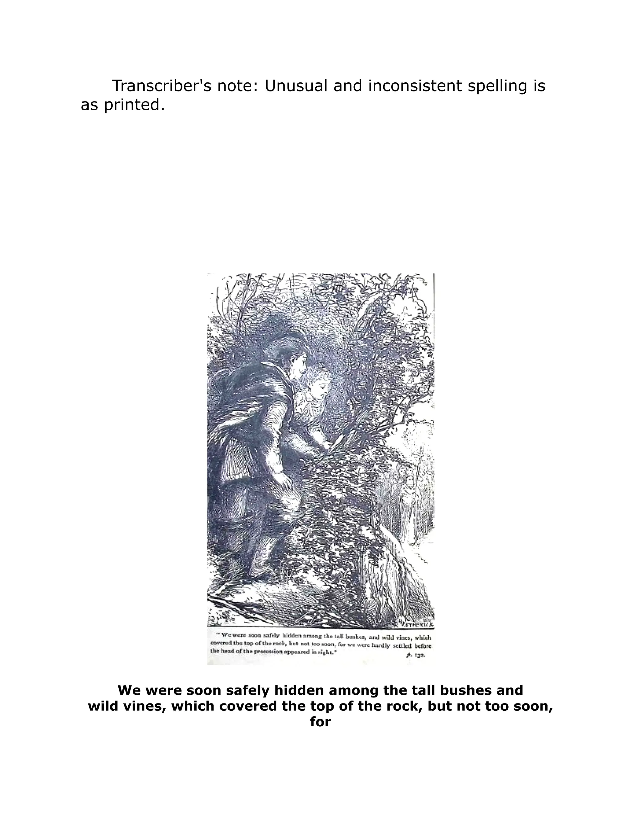
![we were hardly settled before the head of the procession
appeared in sight.
[The Stanton-Corbet Chronicles.]
[Year 1660]
THE
CHEVALIER'S DAUGHTER;
OR,
An Exile for the Truth.
BY
LUCY ELLEN GUERNSEY
AUTHOR OF](https://image.slidesharecdn.com/81267-250225064130-f52b8093/75/Carbon-nanotubes-science-and-applications-1st-Edition-M-Meyyappan-52-2048.jpg)