Microcontroller
8051
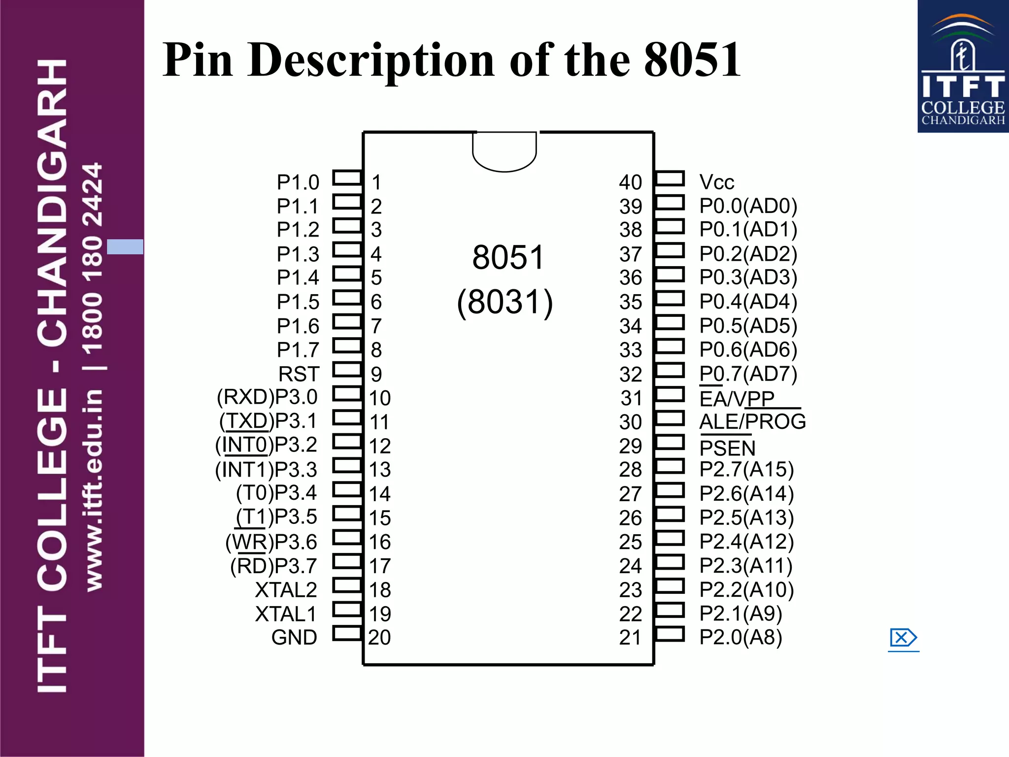
Pin Description of the 8051
1
2
3
4
5
6
7
8
9
10
11
12
13
14
15
16
17
18
19
20
40
39
38
37
36
35
34
33
32
31
30
29
28
27
26
25
24
23
22
21
P1.0
P1.1
P1.2
P1.3
P1.4
P1.5
P1.6
P1.7
RST
(RXD)P3.0
(TXD)P3.1
(T0)P3.4
(T1)P3.5
XTAL2
XTAL1
GND
(INT0)P3.2
(INT1)P3.3
(RD)P3.7
(WR)P3.6
Vcc
P0.0(AD0)
P0.1(AD1)
P0.2(AD2)
P0.3(AD3)
P0.4(AD4)
P0.5(AD5)
P0.6(AD6)
P0.7(AD7)
EA/VPP
ALE/PROG
PSEN
P2.7(A15)
P2.6(A14)
P2.5(A13)
P2.4(A12)
P2.3(A11)
P2.2(A10)
P2.1(A9)
P2.0(A8)
8051
(8031)

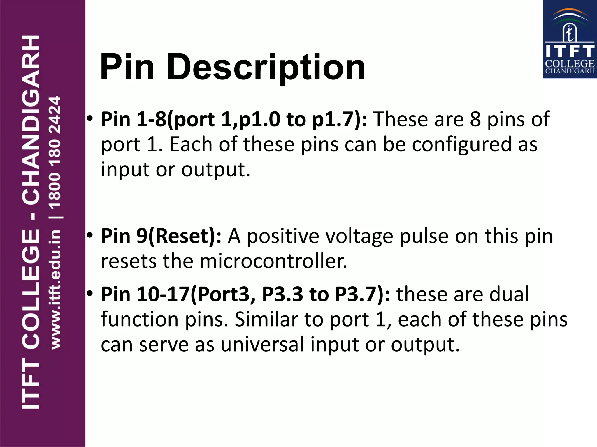
Pin Description
• Pin 1-8(port 1,p1.0 to p1.7): These are 8 pins of
port 1. Each of these pins can be configured as
input or output.
• Pin 9(Reset): A positive voltage pulse on this pin
resets the microcontroller.
• Pin 10-17(Port3, P3.3 to P3.7): these are dual
function pins. Similar to port 1, each of these pins
can serve as universal input or output.
• Pin 18,19 (X1 ,X2): These are the input and
output pins of internal oscillator. A quartz crystal is
usually connected to these pins.
• These 2 pins provide external clock.
• Way 1:using a quartz crystal oscillator
• Way 2:using a TTL oscillator
• Pin 20(GND): Ground
• Pin 21-28(Port2,P2.0 to P2.7): If there is no
intention to use external memory then these port
pins are configured as universal input/output. In
case external memory is used then the higher
address byte ie address A8-A15 will appear on this
port.
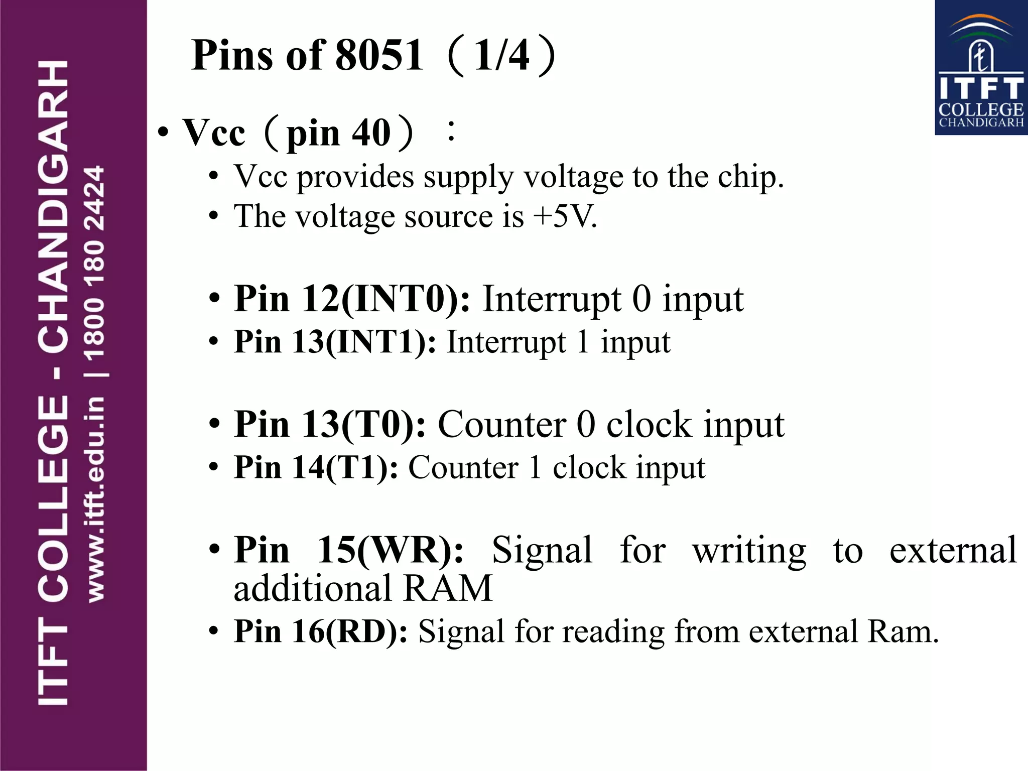
Pins of 8051(1/4)
• Vcc(pin 40):
• Vcc provides supply voltage to the chip.
• The voltage source is +5V.
• Pin 12(INT0): Interrupt 0 input
• Pin 13(INT1): Interrupt 1 input
• Pin 13(T0): Counter 0 clock input
• Pin 14(T1): Counter 1 clock input
• Pin 15(WR): Signal for writing to external
additional RAM
• Pin 16(RD): Signal for reading from external Ram.
Pins of 8051(3/4)
• /EA(pin 31)
• By applying logic 0 to this pin ,P2 and P3 are
used for data and address transmission with no
regards to whether there is internal memory or
not. Otherwise by applying logic 1bto EA pin,
the microcontroller will use both memories, first
internal and afterwards external (if exists) .
• PSEN(pin 29):program store enable
• If external Rom is used for storing program then
it has logic 0 value every time the
microcontroller reads a byte from memory.
Pins of 8051
• ALE(pin 30):address latch enable
• It is an output pin and is active high.
• This pin is used when multiple memory chips are
connected to the controller and only one of them needs
to be selected.
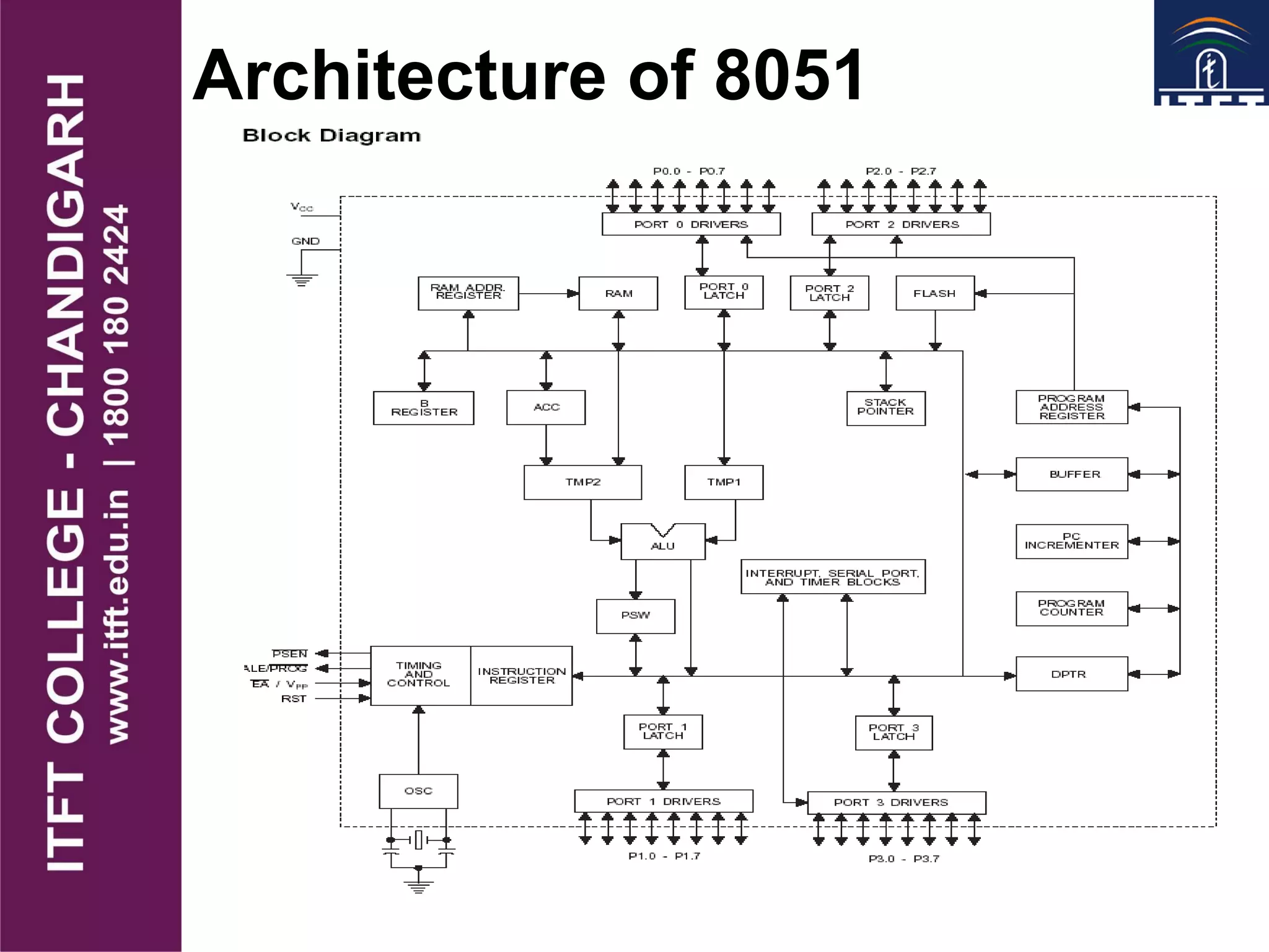
Architecture of 8051

itft-Microcontriller 8051

  • 1.
  • 2.
    Pin Description ofthe 8051 1 2 3 4 5 6 7 8 9 10 11 12 13 14 15 16 17 18 19 20 40 39 38 37 36 35 34 33 32 31 30 29 28 27 26 25 24 23 22 21 P1.0 P1.1 P1.2 P1.3 P1.4 P1.5 P1.6 P1.7 RST (RXD)P3.0 (TXD)P3.1 (T0)P3.4 (T1)P3.5 XTAL2 XTAL1 GND (INT0)P3.2 (INT1)P3.3 (RD)P3.7 (WR)P3.6 Vcc P0.0(AD0) P0.1(AD1) P0.2(AD2) P0.3(AD3) P0.4(AD4) P0.5(AD5) P0.6(AD6) P0.7(AD7) EA/VPP ALE/PROG PSEN P2.7(A15) P2.6(A14) P2.5(A13) P2.4(A12) P2.3(A11) P2.2(A10) P2.1(A9) P2.0(A8) 8051 (8031) 
  • 3.
    Pin Description • Pin1-8(port 1,p1.0 to p1.7): These are 8 pins of port 1. Each of these pins can be configured as input or output. • Pin 9(Reset): A positive voltage pulse on this pin resets the microcontroller. • Pin 10-17(Port3, P3.3 to P3.7): these are dual function pins. Similar to port 1, each of these pins can serve as universal input or output.
  • 4.
    • Pin 18,19(X1 ,X2): These are the input and output pins of internal oscillator. A quartz crystal is usually connected to these pins. • These 2 pins provide external clock. • Way 1:using a quartz crystal oscillator • Way 2:using a TTL oscillator • Pin 20(GND): Ground • Pin 21-28(Port2,P2.0 to P2.7): If there is no intention to use external memory then these port pins are configured as universal input/output. In case external memory is used then the higher address byte ie address A8-A15 will appear on this port.
  • 5.
    Pins of 8051(1/4) •Vcc(pin 40): • Vcc provides supply voltage to the chip. • The voltage source is +5V. • Pin 12(INT0): Interrupt 0 input • Pin 13(INT1): Interrupt 1 input • Pin 13(T0): Counter 0 clock input • Pin 14(T1): Counter 1 clock input • Pin 15(WR): Signal for writing to external additional RAM • Pin 16(RD): Signal for reading from external Ram.
  • 6.
    Pins of 8051(3/4) •/EA(pin 31) • By applying logic 0 to this pin ,P2 and P3 are used for data and address transmission with no regards to whether there is internal memory or not. Otherwise by applying logic 1bto EA pin, the microcontroller will use both memories, first internal and afterwards external (if exists) . • PSEN(pin 29):program store enable • If external Rom is used for storing program then it has logic 0 value every time the microcontroller reads a byte from memory.
  • 7.
    Pins of 8051 •ALE(pin 30):address latch enable • It is an output pin and is active high. • This pin is used when multiple memory chips are connected to the controller and only one of them needs to be selected.
  • 8.