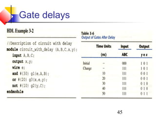
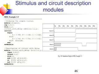
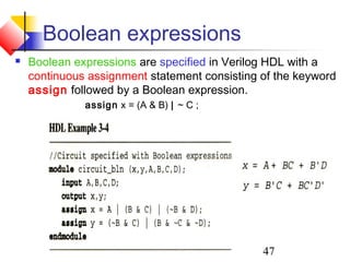
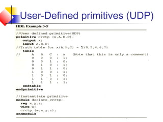
Downloaded 58 times


![29
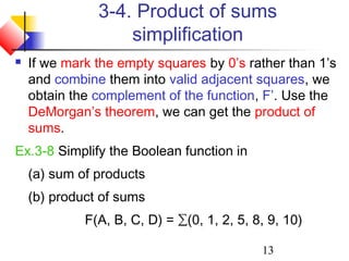
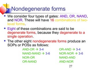
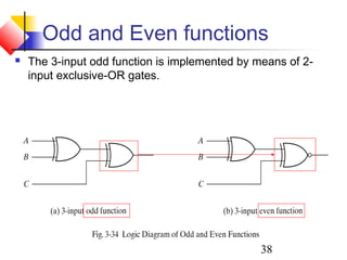
OR-AND-INVERT implementation
The OR-NAND form resembles the OR-AND form, except
for the inversion done by the bubble in the NAND gate.
F = [(A + B)(C + D)E]’
Shift
back](https://image.slidesharecdn.com/chapter-32-160418114721/85/Chapter-3-2-29-320.jpg)

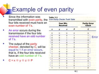
![34
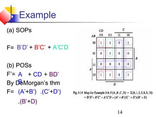
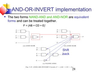
Example
The normal output F
F = (x + y + z)(x’ + y’ + z)]’
We can implement the function in the OR-NAND and NOR-OR
forms as follows.](https://image.slidesharecdn.com/chapter-32-160418114721/85/Chapter-3-2-34-320.jpg)


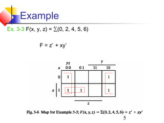
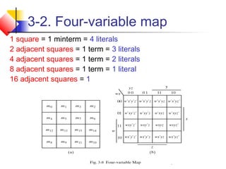
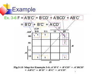
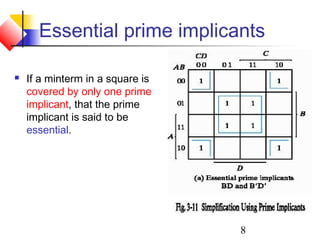
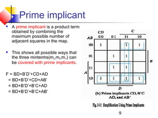
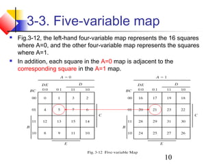
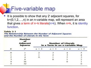
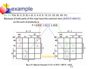
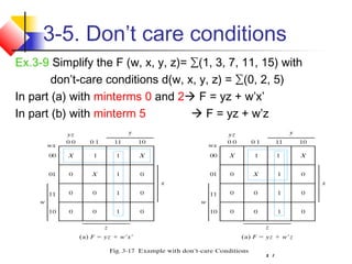
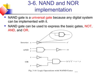
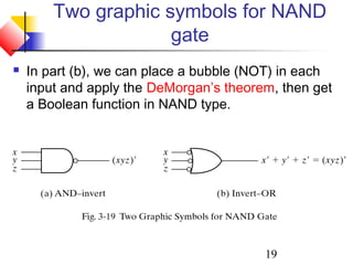
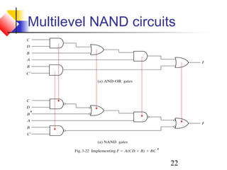
This document provides information about minimizing Boolean functions using Karnaugh maps. It discusses how Karnaugh maps can be used to simplify Boolean expressions into sums of products. Different examples are provided to demonstrate how to minimize functions with 2, 3, 4, and 5 variables using Karnaugh maps. Additional topics covered include don't care conditions, implementing logic with NAND and NOR gates, and exclusive OR functions.