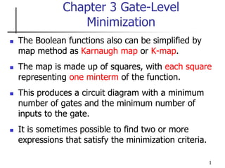
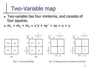
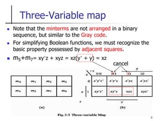
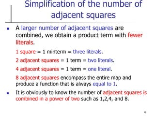
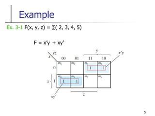
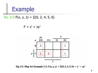
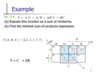
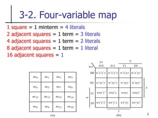
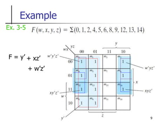
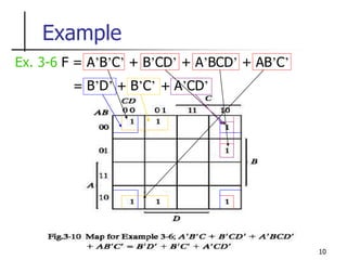
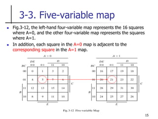
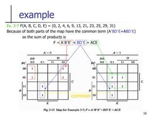
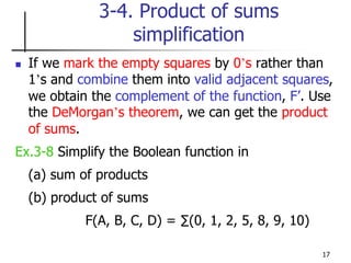
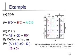
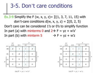
The document discusses Boolean function minimization using Karnaugh maps. It begins by introducing Karnaugh maps and how they are used to simplify Boolean functions into logic circuits with the fewest gates and inputs. Different sized Karnaugh maps are demonstrated, including two-variable, three-variable, and four-variable maps. Techniques for simplifying functions based on the number of adjacent squares in the map are described. Several examples of using Karnaugh maps to minimize Boolean functions are provided.


![35
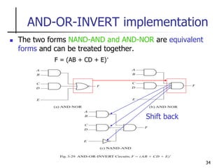
OR-AND-INVERT implementation
The OR-NAND form resembles the OR-AND form, except for
the inversion done by the bubble in the NAND gate.
F = [(A + B)(C + D)E]’
Shift back](https://image.slidesharecdn.com/chapter-3-231226050001-cc6e6671/85/Chapter-3-pptx-35-320.jpg)

![40
Example
The normal output F
F = (x + y + z)(x’ + y’ + z)]’
We can implement the function in the OR-NAND and NOR-OR
forms as follows.](https://image.slidesharecdn.com/chapter-3-231226050001-cc6e6671/85/Chapter-3-pptx-40-320.jpg)