August 26, 2025EASTERN MEDITERRANEAN UNIVERSITY 1
Digital Logic Design I
Gate-Level Minimization
Mustafa Kemal Uyguroğlu
2.
August 26, 2025
2
3-1Introduction
Gate-level minimization refers to the design task of
finding an optimal gate-level implementation of Boolean
functions describing a digital circuit.
3.
August 26, 2025
3
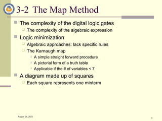
3-2The Map Method
The complexity of the digital logic gates
The complexity of the algebraic expression
Logic minimization
Algebraic approaches: lack specific rules
The Karnaugh map
A simple straight forward procedure
A pictorial form of a truth table
Applicable if the # of variables < 7
A diagram made up of squares
Each square represents one minterm
4.
August 26, 2025
4
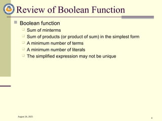
Reviewof Boolean Function
Boolean function
Sum of minterms
Sum of products (or product of sum) in the simplest form
A minimum number of terms
A minimum number of literals
The simplified expression may not be unique
5.
August 26, 2025
5
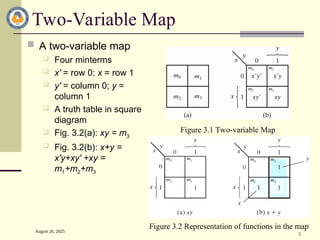
Two-VariableMap
A two-variable map
Four minterms
x' = row 0; x = row 1
y' = column 0; y =
column 1
A truth table in square
diagram
Fig. 3.2(a): xy = m3
Fig. 3.2(b): x+y =
x'y+xy' +xy =
m1+m2+m3
Figure 3.2 Representation of functions in the map
Figure 3.1 Two-variable Map
6.
August 26, 2025
6
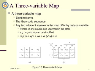
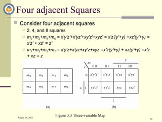
AThree-variable Map
A three-variable map
Eight minterms
The Gray code sequence
Any two adjacent squares in the map differ by only on variable
Primed in one square and unprimed in the other
e.g., m5 and m7 can be simplified
m5+ m7 = xy'z + xyz = xz (y'+y) = xz
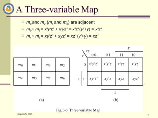
Figure 3.3 Three-variable Map
7.
August 26, 2025
7
AThree-variable Map
m0 and m2 (m4 and m6) are adjacent
m0+ m2 = x'y'z' + x'yz' = x'z' (y'+y) = x'z'
m4+ m6 = xy'z' + xyz' = xz' (y'+y) = xz'
8.
August 26, 2025
8
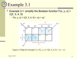
Example3.1
Example 3.1: simplify the Boolean function F(x, y, z) =
(2, 3, 4, 5)
F(x, y, z) = (2, 3, 4, 5) = x'y + xy'
Figure 3.4 Map for Example 3.1, F(x, y, z) = Σ(2, 3, 4, 5) = x'y + xy'
9.
August 26, 2025
9
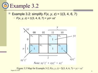
Example3.2
Example 3.2: simplify F(x, y, z) = (3, 4, 6, 7)
F(x, y, z) = (3, 4, 6, 7) = yz+ xz'
Figure 3.5 Map for Example 3-2; F(x, y, z) = Σ(3, 4, 6, 7) = yz + xz'
August 26, 2025
11
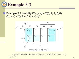
Example3.3
Example 3.3: simplify F(x, y, z) = (0, 2, 4, 5, 6)
F(x, y, z) = (0, 2, 4, 5, 6) = z'+ xy'
Figure 3.6 Map for Example 3-3, F(x, y, z) = Σ(0, 2, 4, 5, 6) = z' +xy'
12.
August 26, 2025
12
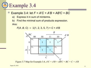
Example3.4
Example 3.4: let F = A'C + A'B + AB'C + BC
a) Express it in sum of minterms.
b) Find the minimal sum of products expression.
Ans:
F(A, B, C)(1, 2, 3, 5, 7) = C + A'B
Figure 3.7 Map for Example 3.4, A'C + A'B + AB'C + BC = C + A'B
13.
August 26, 2025
13
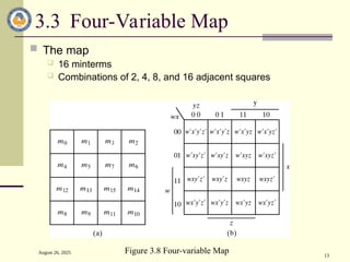
3.3Four-Variable Map
The map
16 minterms
Combinations of 2, 4, 8, and 16 adjacent squares
Figure 3.8 Four-variable Map
14.
August 26, 2025
14
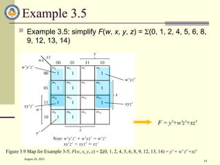
Example3.5
Example 3.5: simplify F(w, x, y, z) = (0, 1, 2, 4, 5, 6, 8,
9, 12, 13, 14)
F = y'+w'z'+xz'
Figure 3.9 Map for Example 3-5; F(w, x, y, z) = Σ(0, 1, 2, 4, 5, 6, 8, 9, 12, 13, 14) = y' + w' z' +xz'
15.
August 26, 2025
15
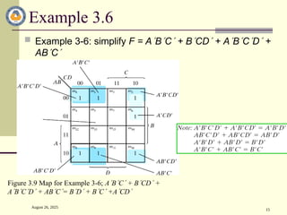
Example3.6
Example 3-6: simplify F = ABC + BCD + ABCD +
ABC
Figure 3.9 Map for Example 3-6; ABC + BCD +
ABCD + ABC= BD + BC +ACD
16.
August 26, 2025
16
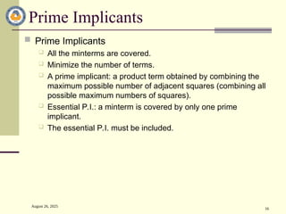
PrimeImplicants
Prime Implicants
All the minterms are covered.
Minimize the number of terms.
A prime implicant: a product term obtained by combining the
maximum possible number of adjacent squares (combining all
possible maximum numbers of squares).
Essential P.I.: a minterm is covered by only one prime
implicant.
The essential P.I. must be included.
17.
August 26, 2025
17
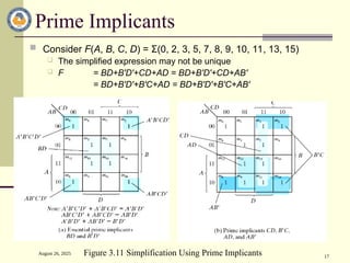
PrimeImplicants
Consider F(A, B, C, D) = Σ(0, 2, 3, 5, 7, 8, 9, 10, 11, 13, 15)
The simplified expression may not be unique
F = BD+B'D'+CD+AD = BD+B'D'+CD+AB'
= BD+B'D'+B'C+AD = BD+B'D'+B'C+AB'
Figure 3.11 Simplification Using Prime Implicants
18.
August 26, 2025
18
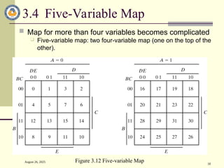
3.4Five-Variable Map
Map for more than four variables becomes complicated
Five-variable map: two four-variable map (one on the top of the
other).
Figure 3.12 Five-variable Map
19.
August 26, 2025
19
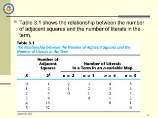
Table 3.1 shows the relationship between the number
of adjacent squares and the number of literals in the
term.
20.
August 26, 2025
20
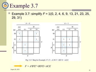
Example3.7
Example 3.7: simplify F = (0, 2, 4, 6, 9, 13, 21, 23, 25,
29, 31)
F = A'B'E'+BD'E+ACE
21.
August 26, 2025
21
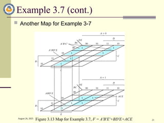
Example3.7 (cont.)
Another Map for Example 3-7
Figure 3.13 Map for Example 3.7, F = A'B'E'+BD'E+ACE
22.
August 26, 2025
22
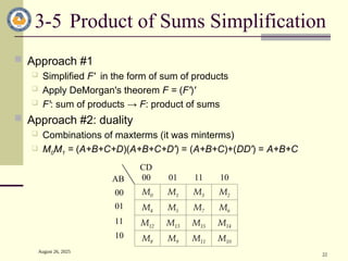
3-5Product of Sums Simplification
Approach #1
Simplified F' in the form of sum of products
Apply DeMorgan's theorem F = (F')'
F': sum of products → F: product of sums
Approach #2: duality
Combinations of maxterms (it was minterms)
M0M1 = (A+B+C+D)(A+B+C+D') = (A+B+C)+(DD') = A+B+C
M0 M1 M3 M2
M4 M5 M7 M6
M12 M13 M15 M14
M8 M9 M11 M10
00
01
11
10
00 01 11 10
AB
CD
23.
August 26, 2025
23
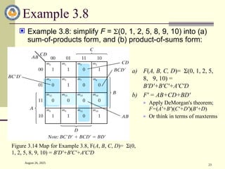
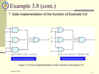
Example3.8
Example 3.8: simplify F = (0, 1, 2, 5, 8, 9, 10) into (a)
sum-of-products form, and (b) product-of-sums form:
Figure 3.14 Map for Example 3.8, F(A, B, C, D)=(0,
1, 2, 5, 8, 9, 10) = B'D'+B'C'+A'C'D
a) F(A, B, C, D)=(0, 1, 2, 5,
8, 9, 10) =
B'D'+B'C'+A'C'D
b) F' = AB+CD+BD'
» Apply DeMorgan's theorem;
F=(A'+B')(C'+D')(B'+D)
» Or think in terms of maxterms
24.
August 26, 2025
24
Example3.8 (cont.)
Gate implementation of the function of Example 3.8
Figure 3.15 Gate Implementation of the Function of Example 3.8
Product-of sums form
Sum-of products form
25.
August 26, 2025
25
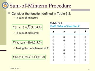
Sum-of-MintermProcedure
Consider the function defined in Table 3.2.
In sum-of-minterm:
In sum-of-maxterm:
Taking the complement of F
( , , ) (1,3,4,6)
F x y z
( , , ) (0,2,5,7)
F x y z
( , , ) ( )( )
F x y z x z x z
26.
August 26, 2025
26
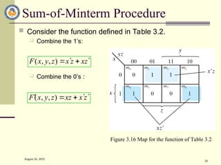
Sum-of-MintermProcedure
Consider the function defined in Table 3.2.
Combine the 1’s:
Combine the 0’s :
( , , )
F x y z x z xz
( , , )
F x y z xz x z
Figure 3.16 Map for the function of Table 3.2
'
27.
August 26, 2025
27
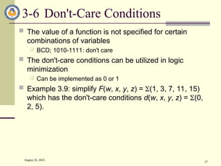
3-6Don't-Care Conditions
The value of a function is not specified for certain
combinations of variables
BCD; 1010-1111: don't care
The don't-care conditions can be utilized in logic
minimization
Can be implemented as 0 or 1
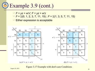
Example 3.9: simplify F(w, x, y, z) = (1, 3, 7, 11, 15)
which has the don't-care conditions d(w, x, y, z) = (0,
2, 5).
28.
August 26, 2025
28
Example3.9 (cont.)
F = yz + w'x'; F = yz + w'z
F = (0, 1, 2, 3, 7, 11, 15) ; F = (1, 3, 5, 7, 11, 15)
Either expression is acceptable
Figure 3.17 Example with don't-care Conditions
29.
August 26, 2025
29
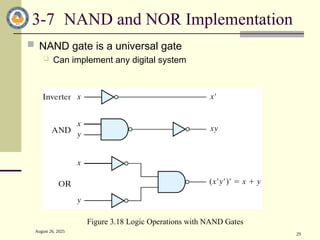
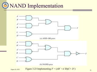
3-7NAND and NOR Implementation
NAND gate is a universal gate
Can implement any digital system
Figure 3.18 Logic Operations with NAND Gates
30.
August 26, 2025
30
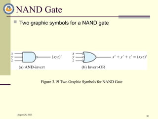
NANDGate
Two graphic symbols for a NAND gate
Figure 3.19 Two Graphic Symbols for NAND Gate
31.
August 26, 2025
31
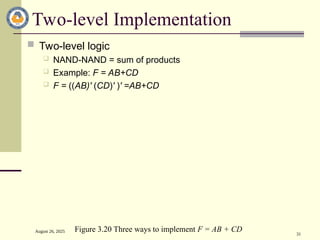
Two-levelImplementation
Two-level logic
NAND-NAND = sum of products
Example: F = AB+CD
F = ((AB)' (CD)' )' =AB+CD
Figure 3.20 Three ways to implement F = AB + CD
32.
August 26, 2025
32
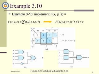
Example3.10
Example 3-10: implement F(x, y, z) =
( , , ) (1,2,3,4,5,7)
F x y z ( , , )
F x y z xy x y z
Figure 3.21 Solution to Example 3-10
33.
August 26, 2025
33
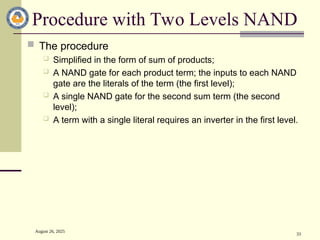
Procedurewith Two Levels NAND
The procedure
Simplified in the form of sum of products;
A NAND gate for each product term; the inputs to each NAND
gate are the literals of the term (the first level);
A single NAND gate for the second sum term (the second
level);
A term with a single literal requires an inverter in the first level.
34.
August 26, 2025
34
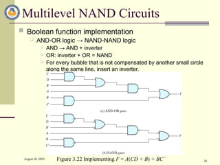
MultilevelNAND Circuits
Boolean function implementation
AND-OR logic → NAND-NAND logic
AND → AND + inverter
OR: inverter + OR = NAND
For every bubble that is not compensated by another small circle
along the same line, insert an inverter.
Figure 3.22 Implementing F = A(CD + B) + BC
August 26, 2025
36
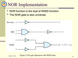
NORImplementation
NOR function is the dual of NAND function.
The NOR gate is also universal.
Figure 3.24 Logic Operation with NOR Gates
37.
August 26, 2025
37
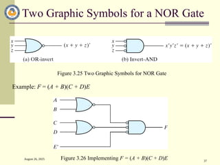
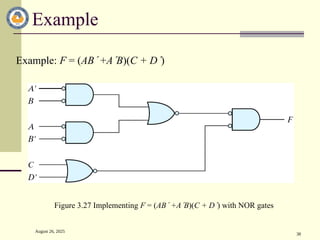
TwoGraphic Symbols for a NOR Gate
Example: F = (A + B)(C + D)E
Figure 3.26 Implementing F = (A + B)(C + D)E
Figure 3.25 Two Graphic Symbols for NOR Gate
August 26, 2025
39
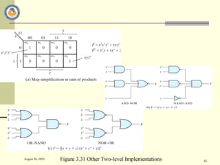
3-8Other Two-level Implementations (
Wired logic
A wire connection between the outputs of two gates
Open-collector TTL NAND gates: wired-AND logic
The NOR output of ECL gates: wired-OR logic
( ) ( ) ( ) ( )( )
( ) ( ) [( )( )]
F AB CD AB CD A B C D
F A B C D A B C D
AND-OR-INVERT function
OR-AND-INVERT function
Figure 3.28 Wired Logic
40.
August 26, 2025
40
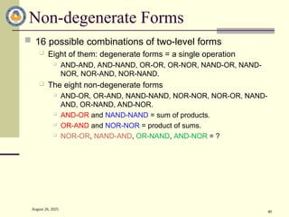
Non-degenerateForms
16 possible combinations of two-level forms
Eight of them: degenerate forms = a single operation
AND-AND, AND-NAND, OR-OR, OR-NOR, NAND-OR, NAND-
NOR, NOR-AND, NOR-NAND.
The eight non-degenerate forms
AND-OR, OR-AND, NAND-NAND, NOR-NOR, NOR-OR, NAND-
AND, OR-NAND, AND-NOR.
AND-OR and NAND-NAND = sum of products.
OR-AND and NOR-NOR = product of sums.
NOR-OR, NAND-AND, OR-NAND, AND-NOR = ?
41.
August 26, 2025
41
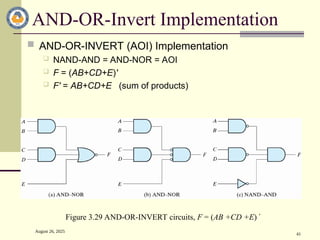
AND-OR-InvertImplementation
AND-OR-INVERT (AOI) Implementation
NAND-AND = AND-NOR = AOI
F = (AB+CD+E)'
F' = AB+CD+E (sum of products)
Figure 3.29 AND-OR-INVERT circuits, F = (AB +CD +E)
42.
August 26, 2025
42
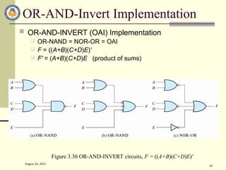
OR-AND-InvertImplementation
OR-AND-INVERT (OAI) Implementation
OR-NAND = NOR-OR = OAI
F = ((A+B)(C+D)E)'
F' = (A+B)(C+D)E (product of sums)
Figure 3.30 OR-AND-INVERT circuits, F = ((A+B)(C+D)E)'
43.
August 26, 2025
43
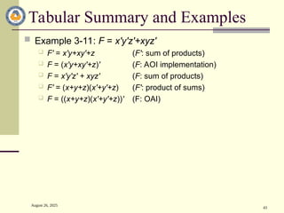
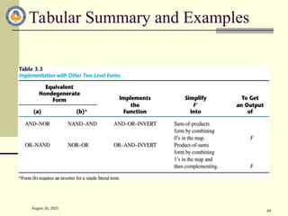
TabularSummary and Examples
Example 3-11: F = x'y'z'+xyz'
F' = x'y+xy'+z (F': sum of products)
F = (x'y+xy'+z)' (F: AOI implementation)
F = x'y'z' + xyz' (F: sum of products)
F' = (x+y+z)(x'+y'+z) (F': product of sums)
F = ((x+y+z)(x'+y'+z))' (F: OAI)
August 26, 2025
48
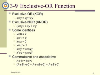
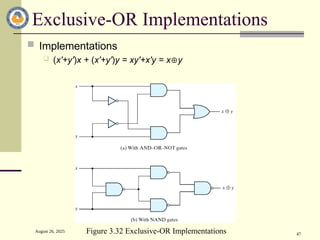
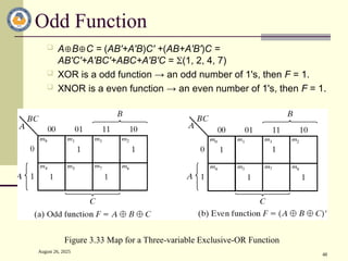
OddFunction
ABC = (AB'+A'B)C' +(AB+A'B')C =
AB'C'+A'BC'+ABC+A'B'C = (1, 2, 4, 7)
XOR is a odd function → an odd number of 1's, then F = 1.
XNOR is a even function → an even number of 1's, then F = 1.
Figure 3.33 Map for a Three-variable Exclusive-OR Function
49.
August 26, 2025
49
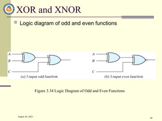
XORand XNOR
Logic diagram of odd and even functions
Figure 3.34 Logic Diagram of Odd and Even Functions
50.
August 26, 2025
50
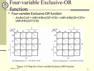
Four-variableExclusive-OR
function
Four-variable Exclusive-OR function
ABCD = (AB'+A'B)(CD'+C'D) = (AB'+A'B)(CD+C'D')+
(AB+A'B')(CD'+C'D)
Figure 3.35 Map for a Four-variable Exclusive-OR Function
51.
August 26, 2025
51
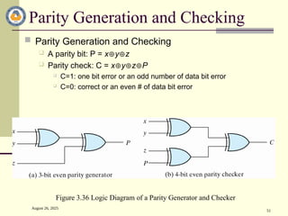
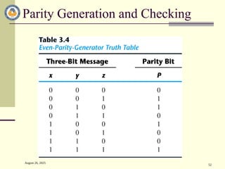
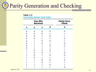
ParityGeneration and Checking
Parity Generation and Checking
A parity bit: P = xyz
Parity check: C = xyzP
C=1: one bit error or an odd number of data bit error
C=0: correct or an even # of data bit error
Figure 3.36 Logic Diagram of a Parity Generator and Checker
August 26, 2025
54
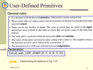
3.10HardwareDescription Language
(HDL)
Describe the design of digital systems in a textual form
Hardware structure
Function/behavior
Timing
VHDL and Verilog HDL
August 26, 2025
56
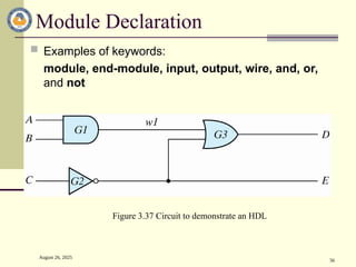
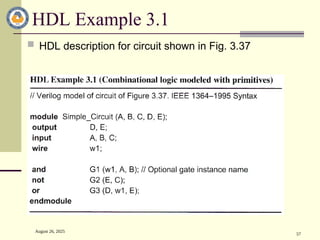
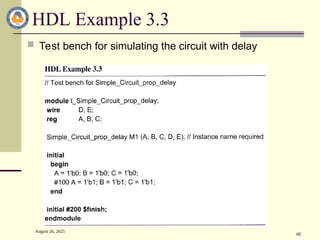
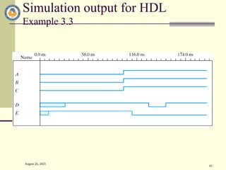
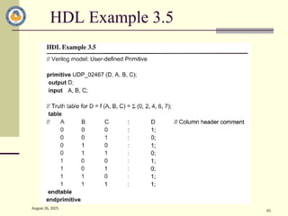
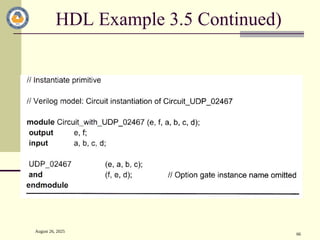
ModuleDeclaration
Examples of keywords:
module, end-module, input, output, wire, and, or,
and not
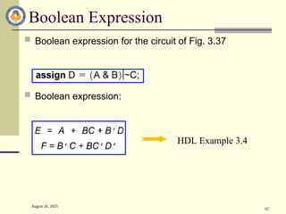
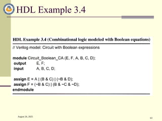
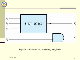
Figure 3.37 Circuit to demonstrate an HDL

![August 26, 2025
39
3-8 Other Two-level Implementations (
Wired logic
A wire connection between the outputs of two gates
Open-collector TTL NAND gates: wired-AND logic
The NOR output of ECL gates: wired-OR logic
( ) ( ) ( ) ( )( )
( ) ( ) [( )( )]
F AB CD AB CD A B C D
F A B C D A B C D
AND-OR-INVERT function
OR-AND-INVERT function
Figure 3.28 Wired Logic](https://image.slidesharecdn.com/chapter3gate-levelminimization-250826205017-a2145c29/85/Logic-Gate-Level-Minimization-techniques-39-320.jpg)