Departamento de TecnologíaElectrónica – Universidad de Sevilla 1
Unit 3. Combinational circuits
Unit 3. Combinational circuits
Digital Electronic Circuits
E.T.S.I. Informática
Universidad de Sevilla
Jorge Juan-Chico <jjchico@dte.us.es> 2010-2020
This work is licensed under the Creative Commons Attribution-ShareAlike 4.0 International License. To view a copy of this license,
visit http://creativecommons.org/licenses/by-sa/4.0/ or send a letter to Creative Commons, PO Box 1866, Mountain View, CA 94042,
USA.
2.
Departamento de TecnologíaElectrónica – Universidad de Sevilla 2
Contents
Contents
●
Logic functions
●
Boolean algebra
●
Combinational design
●
Functional analysis
●
Timing analysis
3.
Departamento de TecnologíaElectrónica – Universidad de Sevilla 3
Learning outcomes
Learning outcomes
●
Use boolean expressions and their canonical and normalized forms.
●
Represent any combinational circuit with truth tables, normalized
boolean expressions and equivalent circuits
●
Recognize combinational problems and be able to define a function
to solve them.
●
Obtain optimized boolean expressions using Karnaugh maps.
●
Implement circuits for normalized boolean expressions using logic
gates.
●
Extract the logic function from a combinational circuit schematic.
●
Represent the evolution in time of the signals in a combinational
circuit using simple delay models.
●
Understand the nature and risks of circuits presenting hazards.
4.
Departamento de TecnologíaElectrónica – Universidad de Sevilla 4
Bibliography
Bibliography
●
Recommended
– LaMeres, chapter 4.
●
Extra exercises from the course's collection 2 (in Spanish)
– Function minimization from truth table: 1
– Function minimization from min(max)terms: 4
– Function minimization with don't cares: 5 (a, b, h)
– Representations: 16
– Design exercises: 7, 10, 19, 23, 24, 25, 26, 27
– Non-standard design: 20
– Functional analysis: 2
– Timing analysis: 14
5.
Departamento de TecnologíaElectrónica – Universidad de Sevilla 5
●
Many problems can be described with digital (0,1) variables:
– on/off, active/inactive, true/false, run/stop, etc.
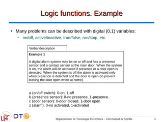
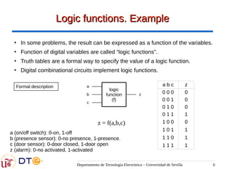
Logic functions. Example
Logic functions. Example
Example 1
A digital alarm system may be on or off and has a presence
sensor and a contact sensor at the main door. When the system
is on, the alarm will be activated if presence or a door open is
detected. When the system is off the alarm is activated only
when presence is detected and the door is open (to prevent
leaving the door open when at home).
Verbal description
a (on/off switch): 0-on, 1-off
b (presence sensor): 0-no presence, 1-presence.
c (door sensor): 0-door closed, 1-door open
z (alarm): 0-no activated, 1-activated
6.
Departamento de TecnologíaElectrónica – Universidad de Sevilla 6
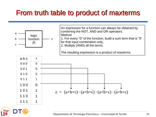
Logic functions. Example
Logic functions. Example
logic
function
(f)
a
b
c
z
a b c z
0 0 0 0
0 0 1 0
0 1 0 0
0 1 1 1
1 0 0 0
1 0 1 1
1 1 0 1
1 1 1 1
Formal description
●
In some problems, the result can be expressed as a function of the variables.
●
Function of digital variables are called “logic functions”.
●
Truth tables are a formal way to specify the value of a logic function.
●
Digital combinational circuits implement logic functions.
a (on/off switch): 0-on, 1-off
b (presence sensor): 0-no presence, 1-presence.
c (door sensor): 0-door closed, 1-door open
z (alarm): 0-no activated, 1-activated
z = f(a,b,c)
7.
Departamento de TecnologíaElectrónica – Universidad de Sevilla 7
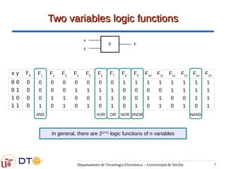
Two variables logic functions
Two variables logic functions
x y F0
F1
F2
F3
F4
F5
F6
F7
F8
F9
F10
F11
F12
F13
F14
F15
0 0 0 0 0 0 0 0 0 0 1 1 1 1 1 1 1 1
0 1 0 0 0 0 1 1 1 1 0 0 0 0 1 1 1 1
1 0 0 0 1 1 0 0 1 1 0 0 1 1 0 0 1 1
1 1 0 1 0 1 0 1 0 1 0 1 0 1 0 1 0 1
F
x
y
F
In general, there are 2(2^n)
logic functions of n variables
AND OR NAND
NOR
XOR XNOR
8.
Departamento de TecnologíaElectrónica – Universidad de Sevilla 8
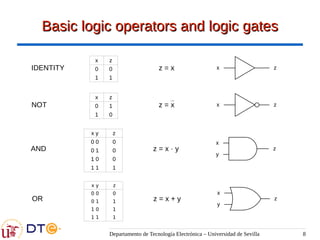
Basic logic operators and logic gates
Basic logic operators and logic gates
AND
OR
z
x
y
x y z
0 0 0
0 1 0
1 0 0
1 1 1
z = x · y
z = x + y
x
y
z
NOT x z
x z
0 1
1 0
z = x
x y z
0 0 0
0 1 1
1 0 1
1 1 1
IDENTITY x z
x z
0 0
1 1
z = x
9.
Departamento de TecnologíaElectrónica – Universidad de Sevilla 9
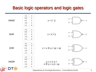
Basic logic operators and logic gates
Basic logic operators and logic gates
NAND
NOR
x
y
z
x y z
0 0 1
0 1 1
1 0 1
1 1 0
x y z
0 0 1
0 1 0
1 0 0
1 1 0
z = x · y
z = x + y
x
y
z
OR
XOR
XNOR
x
y
z
x
y
z
x y z
0 0 0
0 1 1
1 0 1
1 1 0
x y z
0 0 1
0 1 0
1 0 0
1 1 1
z = x ⊕ y = xy + xy
z = x ⊙ y =
x ⊕ y = x y + xy
10.
Departamento de TecnologíaElectrónica – Universidad de Sevilla 10
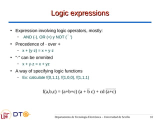
Logic expressions
Logic expressions
●
Expression involving logic operators, mostly:
– AND (·), OR (+) y NOT ( ')
●
Precedence of · over +
– x + (y·z) = x + y·z
●
"·" can be ommited
– x + y·z = x + yz
●
A way of specifying logic functions
– Ex: calculate f(0,1,1), f(1,0,0), f(1,1,1)
f(a,b,c) = (a+b+c) (a + b c) + cd (a+c)
11.
Departamento de TecnologíaElectrónica – Universidad de Sevilla 11
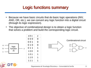
Logic functions summary
Logic functions summary
●
Because we have basic circuits that do basic logic operations (INV,
AND, OR, etc.), we can convert any logic function into a digital circuit
(through its logic expression).
●
The objective of combinational design is to obtain a logic function
that solves a problem and build the corresponding logic circuit.
a b c z
0 0 0 0
0 0 1 0
0 1 0 0
0 1 1 1
1 0 0 0
1 0 1 1
1 1 0 1
1 1 1 1
a
b
c
1
z
Combinational circuit
logic
function
(f)
a
b
c
z
12.
Departamento de TecnologíaElectrónica – Universidad de Sevilla 12
Contents
Contents
●
Logic functions
●
Boolean algebra
●
Combinational design
●
Functional analysis
●
Timing analysis
13.
Departamento de TecnologíaElectrónica – Universidad de Sevilla 13
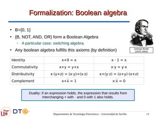
Formalization: Boolean algebra
Formalization: Boolean algebra
●
B={0, 1}
●
{B, NOT, AND, OR} form a Boolean Algebra
– A particular case: switching algebra.
●
Any boolean algebra fulfills this axioms (by definition)
Identity x+0 = x x · 1 = x
Commutativity x+y = y+x x·y = y·x
Distributivity x·(y+z) = (x·y)+(x·z) x+(y·z) = (x+y)·(x+z)
Complement x+x = 1 x·x = 0
George Boole
(1815-1864)
Duality: if an expression holds, the expression that results from
interchanging + with · and 0 with 1 also holds.
14.
Departamento de TecnologíaElectrónica – Universidad de Sevilla 14
Boolean algebra theorems
Boolean algebra theorems
Idempotence x+x = x x·x = x
Complement uniqueness x is unique
Annihilation x+1 = 1 x·0 = 0
Double complement
Absorption x+xy = x x·(x+y) = x
Consensus x+xy = x+y x·(x+y) = x·y
Associativity x+(y+z) = (x+y)+z x·(y·z) = (x·y)·z
De Morgan x·y = x+y x+y = x·y
Reduction xy+xy = x (x+y)(x+y) = x
(x) = x
15.
Departamento de TecnologíaElectrónica – Universidad de Sevilla 15
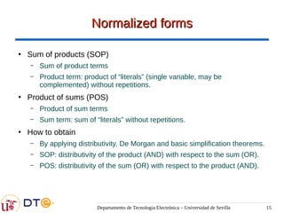
Normalized forms
Normalized forms
●
Sum of products (SOP)
– Sum of product terms
– Product term: product of “literals” (single variable, may be
complemented) without repetitions.
●
Product of sums (POS)
– Product of sum terms
– Sum term: sum of “literals” without repetitions.
●
How to obtain
– By applying distributivity, De Morgan and basic simplification theorems.
– SOP: distributivity of the product (AND) with respect to the sum (OR).
– POS: distributivity of the sum (OR) with respect to the product (AND).
16.
Departamento de TecnologíaElectrónica – Universidad de Sevilla 16
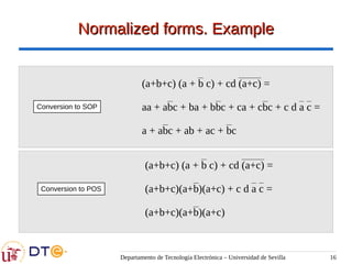
Normalized forms. Example
Normalized forms. Example
(a+b+c) (a + b c) + cd (a+c) =
aa + abc + ba + bbc + ca + cbc + c d a c =
a + abc + ab + ac + bc
Conversion to SOP
(a+b+c) (a + b c) + cd (a+c) =
(a+b+c)(a+b)(a+c) + c d a c =
(a+b+c)(a+b)(a+c)
Conversion to POS
17.
Departamento de TecnologíaElectrónica – Universidad de Sevilla 17
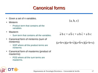
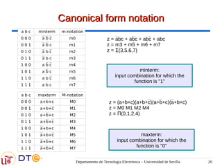
Canonical forms
Canonical forms
●
Given a set of n variables.
●
Minterm
– Product term that contains all the
variables.
●
Maxterm
– Sum term that contains all the variables.
●
Canonical form of minterms (sum of
minterms)
– SOP where all the product terms are
minterms
●
Canonical form of maxterms (product of
maxterms)
– POS where all the sum terms are
maxterms.
{a, b, c}
(a+b+c)(a+b+c)(a+b+c)(a+b+c)
a b c + a b c + a b c + a b c
18.
Departamento de TecnologíaElectrónica – Universidad de Sevilla 18
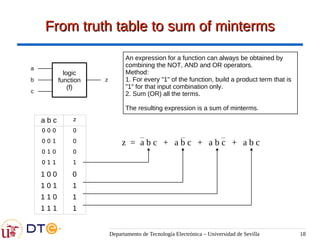
From truth table to sum of minterms
From truth table to sum of minterms
a b c z
0 0 0 0
0 0 1 0
0 1 0 0
0 1 1 1
1 0 0 0
1 0 1 1
1 1 0 1
1 1 1 1
z = a b c + a b c + a b c + a b c
An expression for a function can always be obtained by
combining the NOT, AND and OR operators.
Method:
1. For every "1" of the function, build a product term that is
"1" for that input combination only.
2. Sum (OR) all the terms.
The resulting expression is a sum of minterms.
logic
function
(f)
a
b
c
z
19.
Departamento de TecnologíaElectrónica – Universidad de Sevilla 19
From truth table to product of maxterms
From truth table to product of maxterms
a b c z
0 0 0 0
0 0 1 0
0 1 0 0
0 1 1 1
1 0 0 0
1 0 1 1
1 1 0 1
1 1 1 1
z = (a+b+c)
· ·
(a+b+c) ·
(a+b+c) (a+b+c)
An expression for a function can always be obtained by
combining the NOT, AND and OR operators.
Method:
1. For every "0" of the function, build a sum term that is "0"
for that input combination only.
2. Multiply (AND) all the terms.
The resulting expression is a product of maxterms.
logic
function
(f)
a
b
c
z
20.
Departamento de TecnologíaElectrónica – Universidad de Sevilla 20
Canonical form notation
Canonical form notation
a b c minterm m-notation
0 0 0 a b c m0
0 0 1 a b c m1
0 1 0 a b c m2
0 1 1 a b c m3
1 0 0 a b c m4
1 0 1 a b c m5
1 1 0 a b c m6
1 1 1 a b c m7
z = abc + abc + abc + abc
z = m3 + m5 + m6 + m7
z = Σ(3,5,6,7)
a b c maxterm M-notation
0 0 0 a+b+c M0
0 0 1 a+b+c M1
0 1 0 a+b+c M2
0 1 1 a+b+c M3
1 0 0 a+b+c M4
1 0 1 a+b+c M5
1 1 0 a+b+c M6
1 1 1 a+b+c M7
z = (a+b+c)(a+b+c)(a+b+c)(a+b+c)
z = M0 M1 M2 M4
z = Π(0,1,2,4)
minterm:
input combination for which the
function is "1"
maxterm:
input combination for which the
function is "0"
21.
Departamento de TecnologíaElectrónica – Universidad de Sevilla 21
Conversion between function
Conversion between function
representations
representations
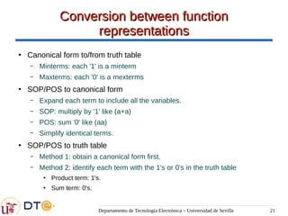
●
Canonical form to/from truth table
– Minterms: each '1' is a minterm
– Maxterms: each '0' is a mexterms
●
SOP/POS to canonical form
– Expand each term to include all the variables.
– SOP: multiply by '1' like (a+a)
– POS: sum '0' like (aa)
– Simplify identical terms.
●
SOP/POS to truth table
– Method 1: obtain a canonical form first.
– Method 2: identify each term with the 1's or 0's in the truth table
●
Product term: 1's.
●
Sum term: 0's.
22.
Departamento de TecnologíaElectrónica – Universidad de Sevilla 22
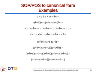
SOP/POS to canonical form
SOP/POS to canonical form
Examples
Examples
a + a b c + ac + bc =
a(b+b)(c+c)+abc+(a+a)bc =
a b c+a b c+a b c+a b c+a b c+a b c+a b c =
a b c + a b c + a b c + a b c + a b c
(a+b+c)(a+b)(a+c) =
(a+b+c)(a+b+cc)(a+c+bb) =
(a+b+c)(a+b+c)(a+b+c)(a+b+c)(a+b+c) =
(a+b+c)(a+b+c)(a+b+c)(a+b+c)
23.
Departamento de TecnologíaElectrónica – Universidad de Sevilla 23
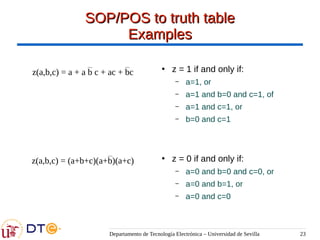
SOP/POS to truth table
SOP/POS to truth table
Examples
Examples
z(a,b,c) = a + a b c + ac + bc
●
z = 1 if and only if:
– a=1, or
– a=1 and b=0 and c=1, of
– a=1 and c=1, or
– b=0 and c=1
●
z = 0 if and only if:
– a=0 and b=0 and c=0, or
– a=0 and b=1, or
– a=0 and c=0
z(a,b,c) = (a+b+c)(a+b)(a+c)
24.
Departamento de TecnologíaElectrónica – Universidad de Sevilla 24
Contents
Contents
●
Logic functions
●
Boolean algebra
●
Combinational design
●
Functional analysis
●
Timing analysis
25.
Departamento de TecnologíaElectrónica – Universidad de Sevilla 25
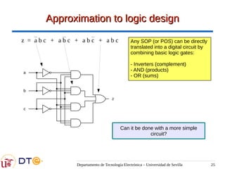
Approximation to logic design
Approximation to logic design
z = a b c + a b c + a b c + a b c
a
b
c
z
Any SOP (or POS) can be directly
translated into a digital circuit by
combining basic logic gates:
- Inverters (complement)
- AND (products)
- OR (sums)
Can it be done with a more simple
circuit?
26.
Departamento de TecnologíaElectrónica – Universidad de Sevilla 26
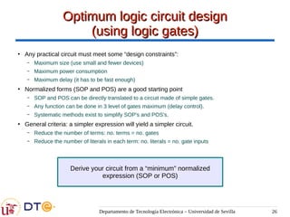
Optimum logic circuit design
Optimum logic circuit design
(using logic gates)
(using logic gates)
●
Any practical circuit must meet some “design constraints”:
– Maximum size (use small and fewer devices)
– Maximum power consumption
– Maximum delay (it has to be fast enough)
●
Normalized forms (SOP and POS) are a good starting point
– SOP and POS can be directly translated to a circuit made of simple gates.
– Any function can be done in 3 level of gates maximum (delay control).
– Systematic methods exist to simplify SOP's and POS's.
●
General criteria: a simpler expression will yield a simpler circuit.
– Reduce the number of terms: no. terms = no. gates
– Reduce the number of literals in each term: no. literals = no. gate inputs
Derive your circuit from a “minimum” normalized
expression (SOP or POS)
27.
Departamento de TecnologíaElectrónica – Universidad de Sevilla 27
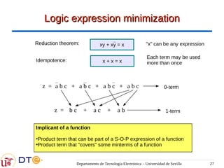
Logic expression minimization
Logic expression minimization
z = a b c + a b c + a b c + a b c
z = b c a c
+ a b
+
Implicant of a function
●
Product term that can be part of a S-O-P expression of a function
●
Product term that "covers" some minterms of a function
0-term
1-term
xy + xy = x "x" can be any expression
Reduction theorem:
Each term may be used
more than once
x + x = x
Idempotence:
28.
Departamento de TecnologíaElectrónica – Universidad de Sevilla 28
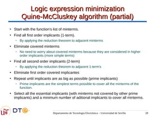
Logic expression minimization
Logic expression minimization
Quine-McCluskey algorithm (partial)
Quine-McCluskey algorithm (partial)
●
Start with the function's list of minterms.
●
Find all first order implicants (1-term).
– By applying the reduction theorem to adjacent minterms
●
Eliminate covered minterms
– No need to worry about covered minterms because they are considered in higher
order implicants (more simple terms)
●
Find all second order implicants (2-term)
– By applying the reduction theorem to adjacent 1-term's
●
Eliminate first order covered implicantes
●
Repeat until implicants are as big as possible (prime implicants)
– Prime implicants are the simplest terms possible to cover all the minterms of the
function.
●
Select all the essential implicants (with minterms not covered by other prime
implicants) and a minimum number of aditional implicants to cover all minterms.
29.
Departamento de TecnologíaElectrónica – Universidad de Sevilla 29
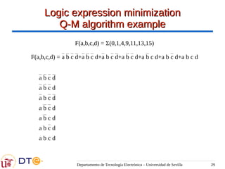
Logic expression minimization
Logic expression minimization
Q-M algorithm example
Q-M algorithm example
F(a,b,c,d) = Σ(0,1,4,9,11,13,15)
F(a,b,c,d) = a b c d+a b c d+a b c d+a b c d+a b c d+a b c d+a b c d
a b c d
a b c d
a b c d
a b c d
a b c d
a b c d
a b c d
30.
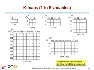
Departamento de TecnologíaElectrónica – Universidad de Sevilla 30
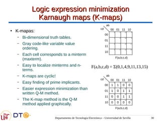
Logic expression minimization
Logic expression minimization
Karnaugh maps (K-maps)
Karnaugh maps (K-maps)
●
K-mapas:
– Bi-dimensional truth tables.
– Gray code-like variable value
ordering.
– Each cell corresponds to a minterm
(maxterm).
– Easy to localize minterms and n-
terms.
– K-maps are cyclic!
– Easy finding of prime implicants.
– Easier expression minimization than
written Q-M method.
– The K-map method is the Q-M
method applied graphically.
F(a,b,c,d) = Σ(0,1,4,9,11,13,15)
01
00
00
01
11
10
10
11
F(a,b,c,d)
cd
ab
0 4 12 8
1 5 13 9
3 7 15 11
2 6 14 10
01
00
00
01
11
10
10
11
F(a,b,c,d)
cd
ab
1
0
1
4
0
12
0
8
1
1
0
5
1
13
1
9
0
3
0
7
1
15
1
11
0
2
0
6
0
14
0
10
Departamento de TecnologíaElectrónica – Universidad de Sevilla 32
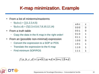
K-map minimization. Example
K-map minimization. Example
●
From a list of minterms/maxterms
– f(a,b,c) = ∑(1,2,3,4,5)
– f(a,b,c,d) = ∏(2,3,4,5,6,7,8,10,12,14)
●
From a truth table
– Copy the data in the K-map in the right order!
●
From an (possible non-minimal) expression
– Convert the expression to a SOP or POS
– Translate the expression to the K-map
– Find minimum SOP/POS
f (a ,b ,c ,d)=(a+b̄)(ac+d)+(b+c)(b̄+d)
a b c z
0 0 0 0
0 0 1 0
0 1 0 1
0 1 1 1
1 0 0 0
1 0 1 1
1 1 0 1
1 1 1 1
33.
Departamento de TecnologíaElectrónica – Universidad de Sevilla 33
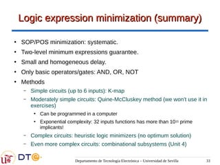
Logic expression minimization (summary)
Logic expression minimization (summary)
●
SOP/POS minimization: systematic.
●
Two-level minimum expressions guarantee.
●
Small and homogeneous delay.
●
Only basic operators/gates: AND, OR, NOT
●
Methods
– Simple circuits (up to 6 inputs): K-map
– Moderately simple circuits: Quine-McCluskey method (we won't use it in
exercises)
●
Can be programmed in a computer
●
Exponential complexity: 32 inputs functions has more than 1015 prime
implicants!
– Complex circuits: heuristic logic minimizers (no optimum solution)
– Even more complex circuits: combinational subsystems (Unit 4)
34.
Departamento de TecnologíaElectrónica – Universidad de Sevilla 34
From minimum SOP/POS to circuit
From minimum SOP/POS to circuit
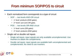
●
Each normalized form corresponds to a type of circuit
– SOP → two levels AND-OR circuit
●
1st level: products (AND gates).
●
2nd level: sum (one OR gate).
– POS → two levels OR-AND circuit
●
1st level: sums (OR gates)
●
2nd level: products (AND gates)
●
Single rail vs double rail inputs
– Single rail inputs: input signals are only available uncomplemented. Use
inverters to obtain the complements.
– Double rail inputs: input signals are available both uncomplemented and
complemented. No need to use inverters.
35.
Departamento de TecnologíaElectrónica – Universidad de Sevilla 35
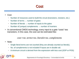
Cost
Cost
●
Cost
– Number of resources used to build the circuit (transistors, resistors, etc.)
– Number of terms → number of gates
– Number of literals → number of inputs to the gates
– Number of (unique) complements → number of inverters
●
In conventional CMOS technology, every input to a gate “costs” two
transistors. In this case, the cost can be estimated like:
●
Note:
– Single literal terms are not counted (they are already counted as literals).
– No. of complements is not included if inputs are in double rail.
– A minimum circuit is derived from the expression with less cost (SOP or POS)
cost=no.terms+no.literals+no.complements
36.
Departamento de TecnologíaElectrónica – Universidad de Sevilla 36
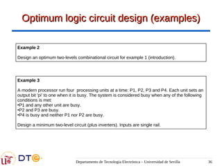
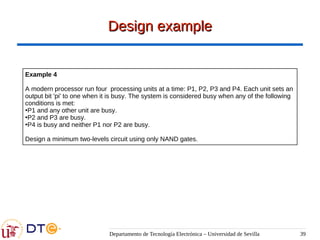
Optimum logic circuit design (examples)
Optimum logic circuit design (examples)
Example 3
A modern processor run four processing units at a time: P1, P2, P3 and P4. Each unit sets an
output bit 'pi' to one when it is busy. The system is considered busy when any of the following
conditions is met:
●
P1 and any other unit are busy.
●
P2 and P3 are busy.
●
P4 is busy and neither P1 nor P2 are busy.
Design a minimum two-level circuit (plus inverters). Inputs are single rail.
Example 2
Design an optimum two-levels combinational circuit for example 1 (introduction).
37.
Departamento de TecnologíaElectrónica – Universidad de Sevilla 37
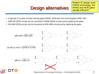
Design alternatives
Design alternatives
●
In general, it is easier to build inverting gates (NAND, NOR) than non-inverting gates (AND, OR).
●
AND-OR (SOP) circuits can be converted to NAND-NAND circuits just by replacing the gates.
●
OR-AND (POS) circuits can be converted to NOR-NOR circuits just by replacing the gates.
ab+cd=(ab)(cd)
(a+b)(c+d)=(a+b)+(c+d)
a
b
c
d
a
b
c
d
a
b
c
d
a
b
c
d
ab+c=(ab)(c)
a
b
c
a
b
c
a
b
c
a
b
c
Modern IC design uses
CMOS technology. Are
NAND and NOR gates
equally efficient?
38.
Departamento de TecnologíaElectrónica – Universidad de Sevilla 38
Optimum simple logic circuit design
Optimum simple logic circuit design
(summary)
(summary)
●
Understand the verbal description of the problem.
●
Clearly define digital inputs and outputs.
●
Make a formal description of the problem: truth table, K-map,
expression, etc.
●
Convert the description to a K-map.
●
Simplify the expression as SOP and/or POS depending on conditions.
●
Convert the expression into a circuit.
– See if you have simple or double rail (affects the cost).
– Consider the cost of SOP and POS.
– Use the appropriate gates depending on conditions: AND, OR, NAND,
NOR, etc.
●
Be clean when drawing the circuit!
39.
Departamento de TecnologíaElectrónica – Universidad de Sevilla 39
Design example
Design example
Example 4
A modern processor run four processing units at a time: P1, P2, P3 and P4. Each unit sets an
output bit 'pi' to one when it is busy. The system is considered busy when any of the following
conditions is met:
●
P1 and any other unit are busy.
●
P2 and P3 are busy.
●
P4 is busy and neither P1 nor P2 are busy.
Design a minimum two-levels circuit using only NAND gates.
40.
Departamento de TecnologíaElectrónica – Universidad de Sevilla 40
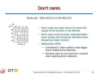
Don't cares
Don't cares
F(a,b,c,d) = Σ(0,1,4,9,11,13,15)+d(2,3,5)
– Don't cares are input values for which the
output of the function is not defined.
– Don't cares make function implementation
more simple and should be identified when
designing a logic function.
– Method (for SOP):
●
Considered '1' when useful to make bigger
(more simple) prime implicants.
●
But don't cares do not need to be “covered”
when selecting prime implicants.
01
00
00
01
11
10
10
11
F(a,b,c,d)
cd
ab
1
0
1
4
0
12
0
8
1
1
-
5
1
13
1
9
-
3
0
7
1
15
1
11
-
2
0
6
0
14
0
10
41.
Departamento de TecnologíaElectrónica – Universidad de Sevilla 41
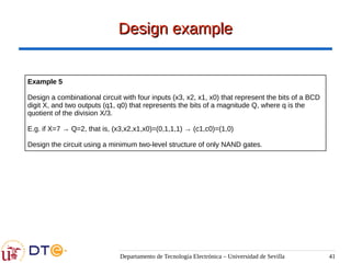
Design example
Design example
Example 5
Design a combinational circuit with four inputs (x3, x2, x1, x0) that represent the bits of a BCD
digit X, and two outputs (q1, q0) that represents the bits of a magnitude Q, where q is the
quotient of the division X/3.
E.g. if X=7 → Q=2, that is, (x3,x2,x1,x0)=(0,1,1,1) → (c1,c0)=(1,0)
Design the circuit using a minimum two-level structure of only NAND gates.
42.
Departamento de TecnologíaElectrónica – Universidad de Sevilla 42
K-map logic circuit design (summary)
K-map logic circuit design (summary)
Formalización
Identificación ent./sal.
Inespecificaciones, etc.
Minimización
“Sólo NAND” → SOP
“Sólo NOR” → POS
“Óptimo” → intentar
SOP&POS
Selección de puertas
¿AND-OR o NAND-NAND?
¿OR-AND o NOR-NOR?
¿Raíl simple o doble?
Descripción funcional
(descripción verbal)
Tabla de verdad/K-mapa
SOP/POS mínimo
Circuito
a
b
c
d
43.
Departamento de TecnologíaElectrónica – Universidad de Sevilla 43
Contents
Contents
●
Logic functions
●
Boolean algebra
●
Combinational design
●
Functional analysis
●
Timing analysis
44.
Departamento de TecnologíaElectrónica – Universidad de Sevilla 44
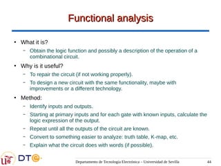
Functional analysis
Functional analysis
●
What it is?
– Obtain the logic function and possibly a description of the operation of a
combinational circuit.
●
Why is it useful?
– To repair the circuit (if not working properly).
– To design a new circuit with the same functionality, maybe with
improvements or a different technology.
●
Method:
– Identify inputs and outputs.
– Starting at primary inputs and for each gate with known inputs, calculate the
logic expression of the output.
– Repeat until all the outputs of the circuit are known.
– Convert to something easier to analyze: truth table, K-map, etc.
– Explain what the circuit does with words (if possible).
45.
Departamento de TecnologíaElectrónica – Universidad de Sevilla 45
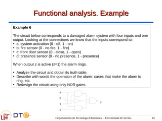
Functional analysis. Example
Functional analysis. Example
z
a
b
c
d
Example 6
The circuit below corresponds to a damaged alarm system with four inputs and one
output. Looking at the connections we know that the inputs correspond to:
●
a: system activation (0 - off, 1 - on)
●
b: fire sensor (0 - no fire, 1 - fire)
●
c: front door sensor (0 - close, 1 - open)
●
d: presence sensor (0 - no presence, 1 - presence)
When output z is active (z=1) the alarm rings.
●
Analyze the circuit and obtain its truth table.
●
Describe with words the operation of the alarm: cases that make the alarm to
ring, etc.
●
Redesign the circuit using only NOR gates.
46.
Departamento de TecnologíaElectrónica – Universidad de Sevilla 46
Contents
Contents
●
Logic functions
●
Boolean algebra
●
Combinational design
●
Functional analysis
●
Timing analysis
47.
Departamento de TecnologíaElectrónica – Universidad de Sevilla 47
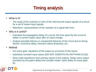
Timing analysis
Timing analysis
●
What is it?
– The study of the evolution in time of the internal and output signals of a circuit
for a set of known input signals.
– Waveform: representation of the variation of a signal with time.
●
Why is it useful?
– Calculate the propagation delay of a circuit: the time spent by the circuit to
obtain a correct output value after an input change.
– Analyze possible failures or unexpected behavior of the circuit due to timing
factors: excessive delay, transient values (hazards), etc.
●
Method
– For every gate: equations of the output as a function of the inputs.
– Substitute constant input values (DO NOT SUBSTITUTE ANYTHING ELSE)
– Draw node waveforms from primary inputs to the outputs. Delay every output
transition by the gate's delay time (simple model: same delay for every gate:
Δ).
48.
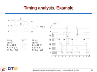
Departamento de TecnologíaElectrónica – Universidad de Sevilla 48
Timing analysis. Example
Timing analysis. Example
x
z
y
f(x,y,z)
A2
A1
I1
I2 y = 1
∆
∆
∆
I1
x
z
I2
A1
A2
f
0 10 20 30 40 50 60 70 80 90 100 t(ns)
I1 = x
I2 = z
A1 = I1 I2
A2 = x y z
f = A1 + A2
I1 = x
I2 = z
A1 = I1 I2
A2 = x z
f = A1 + A2
y = 1
49.
Departamento de TecnologíaElectrónica – Universidad de Sevilla 49
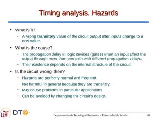
Timing analysis. Hazards
Timing analysis. Hazards
●
What is it?
– A wrong transitory value of the circuit output after inputs change to a
new value.
●
What is the cause?
– The propagation delay in logic devices (gates) when an input affect the
output through more than one path with different propagation delays.
– Their existence depends on the internal structure of the circuit.
●
Is the circuit wrong, then?
– Hazards are perfectly normal and frequent.
– Not harmful in general because they are transitory.
– May cause problems in particular applications.
– Can be avoided by changing the circuit's design.
50.
Departamento de TecnologíaElectrónica – Universidad de Sevilla 50
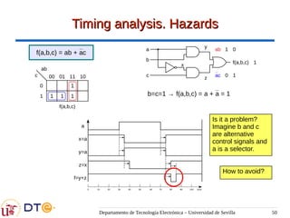
Timing analysis. Hazards
Timing analysis. Hazards
f(a,b,c) = ab + ac
01
00
0
1
10
11
f(a,b,c)
c
ab
1
1 1 1
ab
ac
1
0
0
1
1
b=c=1 → f(a,b,c) = a + a = 1
a
b
c
f(a,b,c)
x
y
z
y=a
a
x=a
z=x
f=y+z
0 10 20 30 40 50 60 70 80 90 100 t(ns)
How to avoid?
Is it a problem?
Imagine b and c
are alternative
control signals and
a is a selector.