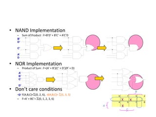
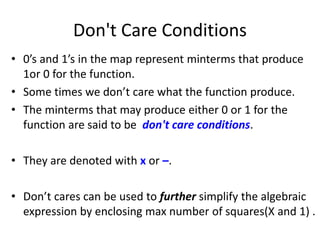
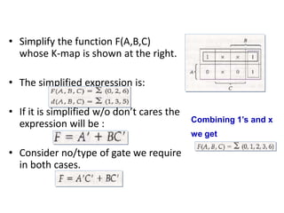
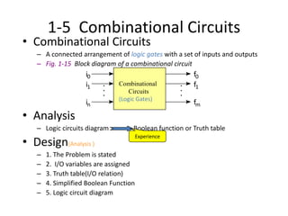
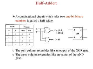
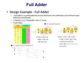
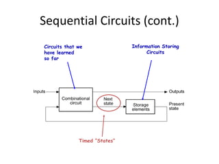
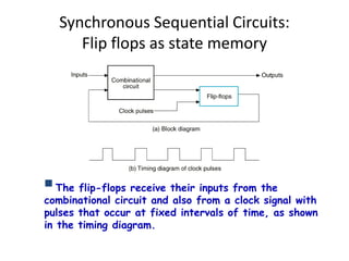
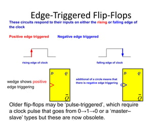
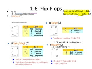
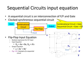
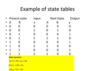
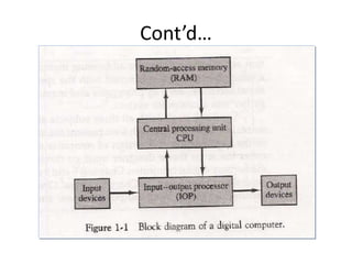
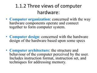
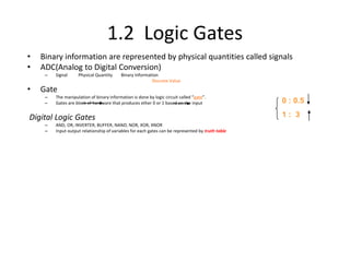
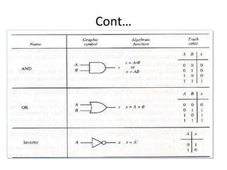
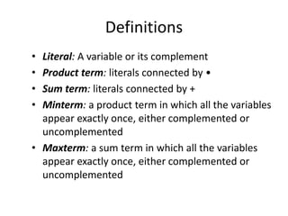
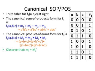
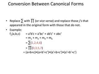
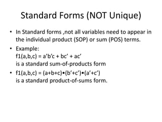
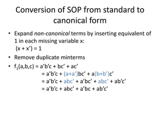
The document provides an in-depth introduction to digital logic circuits, covering the basics of digital computers, hardware and software components, and the principle of binary representation. It explains key concepts such as logic gates, Boolean algebra, and methods for simplifying Boolean expressions, including the use of truth tables and Karnaugh maps. Additionally, it discusses both canonical and standard forms of Boolean functions and their conversion techniques.

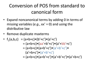
![• []
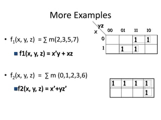
– F= AB’ + C’D + AB’ + C’D
= x + x (let x= AB’ + C’D)
= x
= AB’ + C’D
[]
F= ABC + ABC’ + A’C
= AB(C + C’) + A’C
= AB + A’C
Fig. 1-4 2 graphic symbols for NOR gate
(a) OR-invert (b) invert-OR
Fig. 1-5 2 graphic symbols for NAND gate
(a) NAND-invert (b) invert-NAND
(x+y+z)’
x
y
z
x
y
z
x
y
z
x
y
z
(x’+y’+z’)
(xyz)’
x’ y’z’](https://image.slidesharecdn.com/1stcoa-240607085751-ce28b322/85/Intoduction-to-Computer-Appl-1st_coa-pptx-14-320.jpg)
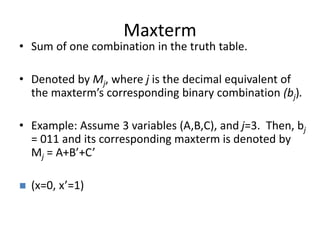
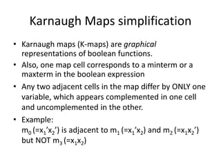
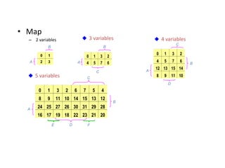
![• [] F= x + y’z
(1) Truth Table
x y z F Minterm
0 0 0 0 m0
0 0 1 1 m1
0 1 0 0 m2
0 1 1 0 m3
1 0 0 1 m4
1 0 1 1 m5
1 1 0 1 m6
1 1 1 1 m7
(2) )
7
,
6
,
5
,
4
,
1
(
)
,
,
(
z
y
x
F
(3)
z
x
y
0 1 3 2
4 5 7 6
F= x + y’z](https://image.slidesharecdn.com/1stcoa-240607085751-ce28b322/85/Intoduction-to-Computer-Appl-1st_coa-pptx-29-320.jpg)
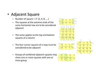
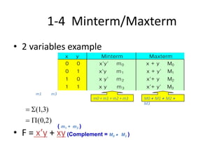
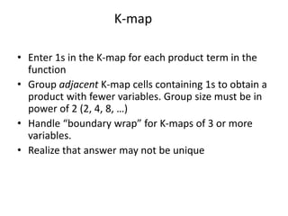
![• []
– F=AC’ + BC
)
7
,
6
,
4
,
3
(
)
,
,
(
C
B
A
F
[]
F=C’ + AB’
)
6
,
5
,
4
,
2
,
0
(
)
,
,
(
C
B
A
F
B
0 1 3 2
4 5 7 6
A
C B
0 1 3 2
4 5 7 6
A
C
A
0 1 3 2
4 5 7 6
12 13 15 14
8 9 11 10
B
C
D
[]
F=C’ + AB’
)
10
,
9
,
8
,
6
,
2
,
1
,
0
(
)
,
,
,
(
D
C
B
A
F
A
0 1 3 2
4 5 7 6
12 13 15 14
8 9 11 10
B
C
D
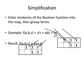
Product-of-Sums Simplification
F=B’D’ + B’C’ + A’C’D
F’=AB + CD + BD’(square marked 0’s)
F’’(F)=(A’ + B’)(C’ + D’)(B’ + D)
)
10
,
9
,
8
,
5
,
2
,
1
,
0
(
)
,
,
,
(
D
C
B
A
F
Sum of product
Product of Sum](https://image.slidesharecdn.com/1stcoa-240607085751-ce28b322/85/Intoduction-to-Computer-Appl-1st_coa-pptx-31-320.jpg)