Download to read offline
![International Refereed Journal of Engineering and Science (IRJES)
ISSN (Online) 2319-183X, (Print) 2319-1821
Volume 2, Issue 1(January 2013), PP.18-24
www.irjes.com
Hardware Implementation of BPSK System on Virtex2-Pro
FPGA Using Xilinx System Generator
Harsha .C.J1 ,Sandeep D.Hanwate2,A.S.Mali3
1(
Electronics Engineering/TKIET/Shivaji University/India)
2(
Electronics Engineering /TKIET/Shivaji University/India)
3(
Electronics Engineering /TKIET/Shivaji University/India)
Abstract: With the recent advent of hardware description languages (e.g., Verilog or VHDL) and digital
implementation for field-programmable gate arrays (FPGAs), substantial academic digital design projects
become practicable. In the present paper, the design of a digital binary-phase-shift-keying (BPSK) modulator
and detector is described. The project details the design of the components (e.g., multiplexer, FIR low pass filter
and comparator) and the simulation of the entire system. The entire system was designed using the Matlab’s
simulink program and system generator block set and implemented on a VIRTEX-2PRO Field Programmable
Gate Array (FPGA) development board. The steps taken to simulate the modulation and demodulation blocks
are shown.
Keywords: Binary phase shift keying (BPSK), Field programmable gate array (FPGA).
I. INTRODUCTION
Digital modulation is the process by which digital symbols are transmitted into waveforms that are
compatible with the characteristics of the channel [2]. The modulation process converts a baseband signal into a
band pass signal compatible with available transmission facilities. At the receiver end, demodulation must be
accomplished to recognize the signals. The process of deciding which symbol was transmitted is referred to as a
detection process. Typically, the receiver generates a signal that is phase-locked to the carrier. Binary-phase-
shift keying (BPSK) does not require but may use a coherent receiver. The coherent receiver is called the
correlation receiver because it correlates the received signal composed of the transmitted signal plus noise with
a sinusoidal signal that is phase-locked to the transmitted carrier. The purpose of the correlation receiver is to
reduce the received symbol to a single point or statistic that is used by the decision circuit to determine which
symbol was transmitted (either 0 or 1). In practice, this single point is a fixed voltage. The decision circuit is a
voltage comparator (digital number comparator) that is set so that if the input voltage (number) is above a
threshold level, the Comparator indicates a “1” is received; if the input voltage (number) is below that level, a
received “0” is indicated [2]. The current project utilizes MATLab simulink language as well as system
generator block set for simulation and implementation on Vertex 2 FPGA development board which mainly
gives the flexibility for designing, testing and makes the development very easy. This process will help in
increasing the design and testing speed of any system within a given time.
II. BPSK MODULATOR AND RECEPTOR
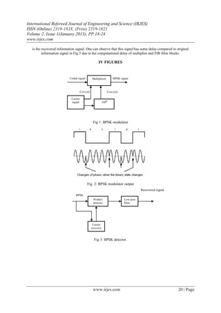
BPSK modulation is the process by which the phase of the carrier is varied in accordance with the
modulating signal.Figure1 shows a simplified block diagram of a BPSK modulator. The coded signal enters to a
multiplexer that commutes the phase of the carrier signal. Depending on the logical condition of the digital
input, the carrier is transferred to the output, either in phase or at 180° outside of phase, with the reference
carrier oscillator [2].
The input signal to the detector can be +cos (ωt) or -cos(ωt). The recovery circuit detects and
regenerates a carrier signal, as in frequency as in phase with the carrier of the original transmitter. The product
detector whose output is the product of the two inputs (the BPSK signal and the recovered carrier). Since the
only possible outputs are the signals cos 2(ωt) and –cos2 (ωt), therefore the product detector’s possible outputs
will be:
cos2 (ωt) = ½ + ½ cos (2ωt),
- cos2 (ωt) = - ½ - ½ cos (2ωt),
Figure 3 shows the blocks diagram of a BPSK receptor. Output of the product detector is given to low pass
(LPF) filter which separates the recovered binary data from the complex demodulated signal [1].
www.irjes.com 18 | Page](https://image.slidesharecdn.com/c211824-130304052020-phpapp02/85/C211824-1-320.jpg)
![International Refereed Journal of Engineering and Science (IRJES)
ISSN (Online) 2319-183X, (Print) 2319-1821
Volume 2, Issue 1(January 2013), PP.18-24
www.irjes.com
Hardware Implementation of BPSK System on Virtex2-Pro
FPGA Using Xilinx System Generator
Harsha .C.J1 ,Sandeep D.Hanwate2,A.S.Mali3
1(
Electronics Engineering/TKIET/Shivaji University/India)
2(
Electronics Engineering /TKIET/Shivaji University/India)
3(
Electronics Engineering /TKIET/Shivaji University/India)
Abstract: With the recent advent of hardware description languages (e.g., Verilog or VHDL) and digital
implementation for field-programmable gate arrays (FPGAs), substantial academic digital design projects
become practicable. In the present paper, the design of a digital binary-phase-shift-keying (BPSK) modulator
and detector is described. The project details the design of the components (e.g., multiplexer, FIR low pass filter
and comparator) and the simulation of the entire system. The entire system was designed using the Matlab’s
simulink program and system generator block set and implemented on a VIRTEX-2PRO Field Programmable
Gate Array (FPGA) development board. The steps taken to simulate the modulation and demodulation blocks
are shown.
Keywords: Binary phase shift keying (BPSK), Field programmable gate array (FPGA).
I. INTRODUCTION
Digital modulation is the process by which digital symbols are transmitted into waveforms that are
compatible with the characteristics of the channel [2]. The modulation process converts a baseband signal into a
band pass signal compatible with available transmission facilities. At the receiver end, demodulation must be
accomplished to recognize the signals. The process of deciding which symbol was transmitted is referred to as a
detection process. Typically, the receiver generates a signal that is phase-locked to the carrier. Binary-phase-
shift keying (BPSK) does not require but may use a coherent receiver. The coherent receiver is called the
correlation receiver because it correlates the received signal composed of the transmitted signal plus noise with
a sinusoidal signal that is phase-locked to the transmitted carrier. The purpose of the correlation receiver is to
reduce the received symbol to a single point or statistic that is used by the decision circuit to determine which
symbol was transmitted (either 0 or 1). In practice, this single point is a fixed voltage. The decision circuit is a
voltage comparator (digital number comparator) that is set so that if the input voltage (number) is above a
threshold level, the Comparator indicates a “1” is received; if the input voltage (number) is below that level, a
received “0” is indicated [2]. The current project utilizes MATLab simulink language as well as system
generator block set for simulation and implementation on Vertex 2 FPGA development board which mainly
gives the flexibility for designing, testing and makes the development very easy. This process will help in
increasing the design and testing speed of any system within a given time.
II. BPSK MODULATOR AND RECEPTOR
BPSK modulation is the process by which the phase of the carrier is varied in accordance with the
modulating signal.Figure1 shows a simplified block diagram of a BPSK modulator. The coded signal enters to a
multiplexer that commutes the phase of the carrier signal. Depending on the logical condition of the digital
input, the carrier is transferred to the output, either in phase or at 180° outside of phase, with the reference
carrier oscillator [2].
The input signal to the detector can be +cos (ωt) or -cos(ωt). The recovery circuit detects and
regenerates a carrier signal, as in frequency as in phase with the carrier of the original transmitter. The product
detector whose output is the product of the two inputs (the BPSK signal and the recovered carrier). Since the
only possible outputs are the signals cos 2(ωt) and –cos2 (ωt), therefore the product detector’s possible outputs
will be:
cos2 (ωt) = ½ + ½ cos (2ωt),
- cos2 (ωt) = - ½ - ½ cos (2ωt),
Figure 3 shows the blocks diagram of a BPSK receptor. Output of the product detector is given to low pass
(LPF) filter which separates the recovered binary data from the complex demodulated signal [1].
www.irjes.com 18 | Page](https://image.slidesharecdn.com/c211824-130304052020-phpapp02/75/C211824-1-2048.jpg)
![International Refereed Journal of Engineering and Science (IRJES)
ISSN (Online) 2319-183X, (Print) 2319-1821
Volume 2, Issue 1(January 2013), PP.18-24
www.irjes.com
III. SIMULINK AND SYSTEM GENERATOR.
The simulation of BPSK system was done using Simulink and the components of System Generator
[1]. The following tools are necessary for the simulation and implementation:
1.Simulink Blockset
Pulse Generator: it simulates a train of pulses.
Scope: oscilloscope used to visualize the results.
Sine Wave: it generates sine functions.
2.System Generator Blockset
Mcode: it calls a Matlab .m file and executes it inside the simulation.
Gateway In: it makes an approach to the behavior of a signal in hardware.
Gateway Out: it returns an approach of the behavior of a signal in hardware to the simulation mode.
Mult: it carries out the multiplication of its two inputs.
FIR: it simulates a FIR Filter, making a call to the Matlab FDATool.
System Generator: It provides control of the system and simulation parameters. It is used to invoke the
generated code.
Resource Estimator: it presents the resources of the device used in the simulation of the circuit.
FDATool: Filter Design and Analysis tool.
3.System Generator
It is a software tool that allows to create and to verify hardware designs for Xilinx FPGAs; it works
together with Simulink and Matlab. It also allows the inclusion of DSP tools to design with FPGAs, automatic
generation of HDL code starting from a Simulink model and allows the user to create its own libraries [6].
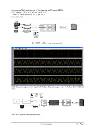
4.Simulation of BPSK modulator
The design of BPSK system using above mentioned tools and its implementation on a FPGA
development board is discussed below. The Figure 4 shows the BPSK modulator designed using matlab
simulink block sets and xilinx system generator blocks [1].
The train of pulse signal generated by pulse generator enters the BPSK multiplexer (Mcode) block that works as
multiplexer between the two Carrier signals (cos (ωt) and -cos (ωt)) depending on the binary values of the signal
to be transmitted. This Mcode block makes a call to an .m file which contains the programming of the
multiplexer. The code, allows us to obtain an output carrier signal of 00 phase shift (a cosine in this case), when
the input is a level of high voltage, and a dephased cosine signal of exit (i.e. carrier signal of 180 0 phase shift)
when the input is a level of low voltage. This high or low state is given by the signal that contains the
information. The output signal of the multiplexer is the modulated one and is ready to be thrown to the channel.
Figure 5 below shows Information signal, carrier signal with 0 0 phase shift, carrier signal with 18 00 phase shift
and BPSK Modulated signal obtained at the output of multiplexer.
5.Simulation of BPSK detector
The modulated signal is transmitted through the AWGN channel and it is given to the detector.The
demodulation is performed according to the scheme [1] shown below in Figure 6.To demodulate the signal
coming from the channel, a (Mult) block that multiplies the signal for the recovered carrier is used.The pass-low
filter FIR separates the continuous signal of ± ½ amplitude recovered from the demodulated complex signal and
allows to select the zero frequency signal (+1/2 or -1/2).
This filter is obtained making a call to the Matlab FDATool that is an interface that allows designing a pass-low
filter. Since at the output of the filter there are signals with ±½ amplitude and with ruffled border in each pulse.
The comparator block makes the call to the .m file, which contains the program of the comparator. This code,
allows us to obtain at the output a voltage level 1, when the input is higher than certain reference voltage in this
case 0V and a level voltage 0 when the input is lower than such reference voltage.
The simulated demodulated process is presented in Figure 7.The first Figure represents the modulated
signal.Second Figure represents the modulated signal after passing through the AWGN channel.Third Figure
represents the signal obtained at the output of multiplier.Fourth Figure represents the recovered signal at the
output of the pass-low filter.Finally the fifth Figure represents the signal at the output of the comparison, and it
www.irjes.com 19 | Page](https://image.slidesharecdn.com/c211824-130304052020-phpapp02/85/C211824-2-320.jpg)
![International Refereed Journal of Engineering and Science (IRJES)
ISSN (Online) 2319-183X, (Print) 2319-1821
Volume 2, Issue 1(January 2013), PP.18-24
www.irjes.com
Fig 10: Modulation-Demodulation process. Result given by development board.
V. BIT ERROR RATE CALCULATION
The bit error rate for the above BPSK design [4] is calculated by making a call to the BERtool in the
MATLAB command window.
Making use of the above tool the bit error rate curves (BER) for the various values of the signal to noise ratio
(SNR) of an Additive white Gaussian noise (AWGN) channel and sampling bits are shown in Figure 8 . BER
curves for 00, 250 ,450,600 and 900 phase shift of a reference carrier signal are shown in Figure 8. From the
Figure 8 it is clear that the bit error rate increases with the increase in the phase difference of the reference
carrier signal as well as increase in signal to noise ratio (SNR).
VI. HARDWARE IMPLEMENTATION
The modulator and detector is implemented on Virtex2-PRO development board .An FPGA consists
on arrangements of several programmable blocks (logical blocks) which are interconnected between themselves
with input/output cells by means of vertical and horizontal connection channels [5].
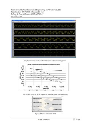
1.Program Tools for the Implementation
For the implementation of the BPSK modulator and demodulator, after simulation, a tool offered by
Xilinx, JTAG Co-Simulator is used; this block allows the co-simulation of the design in the development board.
2. JTAG-Co-simulator
It allows performing hardware Co-simulation using JTAG and a parallel cable or platform USB. When
a model is implemented for JTAG hardware Co-simulation, a new library is created that contains a custom
JTAG Co-simulation block with ports that match the gateway names from the original model, shown in Figure
9.By double-clicking in this block, one can select the most convenient simulation options. Once added to the
design, we should verify that the development board is correctly connected to the computer. Then run the
simulation.The result of the simulation is compared with the results given by the actual implementation. This
www.irjes.com 23 | Page](https://image.slidesharecdn.com/c211824-130304052020-phpapp02/85/C211824-6-320.jpg)
![International Refereed Journal of Engineering and Science (IRJES)
ISSN (Online) 2319-183X, (Print) 2319-1821
Volume 2, Issue 1(January 2013), PP.18-24
www.irjes.com
allows us to verify how close the simulation was to the real implementation. The Figure .10 shows the results of
the hardware implemented BPSK system. One can observe that the results obtained in the development board
are practically the same that those obtained in the previous simulation.
VII. CONCLUSIONS
In this project, BPSK system with modulator and demodulator has been designed and tested. While
testing the detector, the delay in the recovered data at the output of the detector is observed, and it is found that
the delay is due to the computational delay of multiplier and FIR filter blocks. The results given by the
development board exactly matches with the results obtained from simulation setup. From the above results it
may be concluded that the entire result given by the development board is same as that of the result obtained
from the simulation setup. It is also concluded that BER of the BPSK system increases with the increase in the
imperfect phase synchronization of the reference carrier signal as well as SNR of AWGN channel at the
detector. System Generator and Simulink tools offer a simplified environment for the simulation of
communication systems in general. Since the results obtained in hardware are dependent of the design in
software, it is much simpler to carry out changes in these results by means of the software, even after having
finished the design and its implementation. This fact is considered one of the most important in the development
of this type of design.
REFERENCES
[1] Johanna.S, Ruque, David.Ruiz, Carlos, “Simulation and implementation of BPSK system on a FPGA
board using system generator blockset for DSP/FPGA”, School of Electronics and Communication,
Technical university Loja 2005.
[2] B.Sklar, “DigitalCommunications Fundamentals and Applications”, 2nd ed. Englewood Cliffs, NJ:
Prentice-Hall PTR, 2001
[3] Faruque Ahamed and Frank A. Scarpino “An Educational Digital Communications Project to
Implement a BPSK Detector”, IEEE Trans. Commun., vol. COM-34, no. 5, pp. 423–429, May 2000.
[4] F. M. Gardner, “BPSK/QPSK timing-error detector for sampled receivers,” IEEE Trans. Commun., vol.
COM-34, no. 5, pp. 423–429, May 2000.
[5]. C .Britton Rorabaugh “Simulating Wireless Communication Systems”, second edition, Prentice-Hall
Publication, 2004.
[6] L.W.Couch,“Digital and Analog Communication Systems”, seventh Edition, Pearson Publication, 2007.
www.irjes.com 24 | Page](https://image.slidesharecdn.com/c211824-130304052020-phpapp02/85/C211824-7-320.jpg)

This paper presents the design and implementation of a Binary Phase Shift Keying (BPSK) modulator and detector using MATLAB Simulink and Xilinx System Generator on a Virtex-2 Pro FPGA development board. The authors detail the components involved, the simulation processes, and the results of the hardware implementation, which closely matched the simulation outcomes. The study concludes that the Bit Error Rate (BER) of the BPSK system increases with signal-to-noise ratio and imperfect phase synchronization.