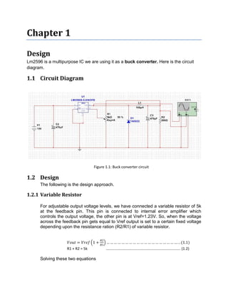
Chapter 1
Design
Lm2596 is a multipurpose IC we are using it as a buck converter. Here is the circuit
diagram.
1.1 Circuit Diagram
Figure 1.1: Buck converter circuit
1.2 Design
The following is the design approach.
1.2.1 Variable Resistor
For adjustable output voltage levels, we have connected a variable resistor of 5k
at the feedback pin. This pin is connected to internal error amplifier which
controls the output voltage, the other pin is at Vref=1.23V. So, when the voltage
across the feedback pin gets equal to Vref output is set to a certain fixed voltage
depending upon the resistance ration (R2/R1) of variable resistor.
= 1 + … … … … … … … … … … … … … … … … … … … . . (1.1)
R1 + R2 = 5k ………………………………………………………………….… (1.2)
Solving these two equations
3.3 V : R1=1.88k , R2=3.12k
5 V : R1=1.25k , R2=3.75k
12 V : R1=0.50k , R2=4.50k
1.2.2 High frequency Diode
Diode is present to provide the return path when switch is off. Since internal
oscillator is operating at 150 kHz so we need a high frequency diode. Currently
we are using 1N5822 shotkey diode (2A).
1.2.3 Input Capacitor
Input capacitor is there to smooth output voltage. Its value should be large. We
selected the value of 470uF. As we increase the value of Capacitor our input
voltage will be smoother.
1.2.4 Output Capacitor
Output capacitor is present to filter the high frequency ripple in output Voltage. As
per data sheet of LM2596
∆ = ∆ ∗ ∗ ∗ … … … … … … … … ..							(1.3)
∆ = 5 	∆ = 250 	 ≤ 0.02	 Capacitor with high voltage and
capacitance has low ESR value so selecting 470uF (50V).
1.2.5 Inductor
Inductor is used in combination of output capacitor to filter the square pulse
output of switch to DC. Since frequency is very high (150 kHz) we assume the
inductor current to be linear.
= ∆ ∗ − −
Where Vs=1.16V (Saturation voltage)
=
∆ ∗
+
Where Vd = 0.5V
1
= +
After Solving
= ( − − ) ∗
+
∗ ∆ ∗ ( − − )
= 12 	∆ = 250 	 ≥ 167
1.3 Modes of Operation
LM2596 have two modes of operations.
1.3.1 Continuous mode
In this mode the current through inductor is continuous. The switch output in this
mode is simple pulse shaped. Usually large load current exist in this mode. The
design values are same as above.
1.3.2 Discontinuous mode
In this mode the current through inductor drops to zero for some time. We can
bring the LM2596 in discontinuous mode by either inductor value below critical
value or decrease load current. When inductor current goes zero neither switch
nor diode conducts, hence a small amount of energy circulate between inductor
and diode. Stray capacitance causes ringing effect at output pin. Overall design
remains same but the value of inductor decreases to one third.
1.4 Under Voltage Lockout
This is the feature which keeps the IC off until the input voltage reaches a certain
threshold level. LM2596 ON/OFF pin serves this purpose. It remains ON if Vin is
less than 1.6V. During OFF state it consumes only 80 uA.
buck_report

buck_report

  • 1.
    Chapter 1 Design Lm2596 isa multipurpose IC we are using it as a buck converter. Here is the circuit diagram. 1.1 Circuit Diagram Figure 1.1: Buck converter circuit 1.2 Design The following is the design approach. 1.2.1 Variable Resistor For adjustable output voltage levels, we have connected a variable resistor of 5k at the feedback pin. This pin is connected to internal error amplifier which controls the output voltage, the other pin is at Vref=1.23V. So, when the voltage across the feedback pin gets equal to Vref output is set to a certain fixed voltage depending upon the resistance ration (R2/R1) of variable resistor. = 1 + … … … … … … … … … … … … … … … … … … … . . (1.1) R1 + R2 = 5k ………………………………………………………………….… (1.2) Solving these two equations
  • 2.
    3.3 V :R1=1.88k , R2=3.12k 5 V : R1=1.25k , R2=3.75k 12 V : R1=0.50k , R2=4.50k 1.2.2 High frequency Diode Diode is present to provide the return path when switch is off. Since internal oscillator is operating at 150 kHz so we need a high frequency diode. Currently we are using 1N5822 shotkey diode (2A). 1.2.3 Input Capacitor Input capacitor is there to smooth output voltage. Its value should be large. We selected the value of 470uF. As we increase the value of Capacitor our input voltage will be smoother. 1.2.4 Output Capacitor Output capacitor is present to filter the high frequency ripple in output Voltage. As per data sheet of LM2596 ∆ = ∆ ∗ ∗ ∗ … … … … … … … … .. (1.3) ∆ = 5 ∆ = 250 ≤ 0.02 Capacitor with high voltage and capacitance has low ESR value so selecting 470uF (50V). 1.2.5 Inductor Inductor is used in combination of output capacitor to filter the square pulse output of switch to DC. Since frequency is very high (150 kHz) we assume the inductor current to be linear. = ∆ ∗ − − Where Vs=1.16V (Saturation voltage) = ∆ ∗ + Where Vd = 0.5V 1 = +
  • 3.
    After Solving = (− − ) ∗ + ∗ ∆ ∗ ( − − ) = 12 ∆ = 250 ≥ 167 1.3 Modes of Operation LM2596 have two modes of operations. 1.3.1 Continuous mode In this mode the current through inductor is continuous. The switch output in this mode is simple pulse shaped. Usually large load current exist in this mode. The design values are same as above. 1.3.2 Discontinuous mode In this mode the current through inductor drops to zero for some time. We can bring the LM2596 in discontinuous mode by either inductor value below critical value or decrease load current. When inductor current goes zero neither switch nor diode conducts, hence a small amount of energy circulate between inductor and diode. Stray capacitance causes ringing effect at output pin. Overall design remains same but the value of inductor decreases to one third. 1.4 Under Voltage Lockout This is the feature which keeps the IC off until the input voltage reaches a certain threshold level. LM2596 ON/OFF pin serves this purpose. It remains ON if Vin is less than 1.6V. During OFF state it consumes only 80 uA.