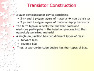
SlideShare a Scribd company logo
1 of 44
Bipolar Junction Transistor
(BJT)
CHAPTER 3
Introduction
• The basic of electronic system nowadays is
semiconductor device.
• The famous and commonly use of this device
is BJTs
(Bipolar Junction Transistors).
• It can be use as amplifier and logic switches.
• BJT consists of three terminal:
 collector : C
 base : B
emitter : E
• Two types of BJT : pnp and npn
Transistor Construction
• 3 layer semiconductor device consisting:
• 2 n- and 1 p-type layers of material  npn transistor
• 2 p- and 1 n-type layers of material pnp transistor
• The term bipolar reflects the fact that holes and
electrons participate in the injection process into the
oppositely polarized material
• A single pn junction has two different types of bias:
• forward bias
• reverse bias
• Thus, a two-pn-junction device has four types of bias.
Position of the terminals and symbol
of BJT.
• Base is located at the middle
and more thin from the level
of collector and emitter
• The emitter and collector
terminals are made of the
same type of semiconductor
material, while the base of the
other type of material
Transistor currents
-The arrow is always drawn
on the emitter
-The arrow always point
toward the n-type
-The arrow indicates the
direction of the emitter
current:
pnp:E B
npn: B E
IC=the collector current
IB= the base current
IE= the emitter current
• By imaging the analogy of diode, transistor can be
construct like two diodes that connetecd together.
• It can be conclude that the work of transistor is base on
work of diode.
Transistor Operation
• The basic operation will be described using the pnp
transistor. The operation of the pnp transistor is
exactly the same if the roles played by the electron
and hole are interchanged.
• One p-n junction of a transistor is reverse-biased,
whereas the other is forward-biased.
Forward-biased junction
of a pnp transistor
Reverse-biased junction
of a pnp transistor
• Both biasing potentials have been applied to a pnp
transistor and resulting majority and minority carrier
flows indicated.
• Majority carriers (+) will diffuse across the forward-
biased p-n junction into the n-type material.
• A very small number of carriers (+) will through n-type
material to the base terminal. Resulting IB is typically in
order of microamperes.
• The large number of majority carriers will diffuse across
the reverse-biased junction into the p-type material
connected to the collector terminal.
• Majority carriers can cross the reverse-biased
junction because the injected majority carriers will
appear as minority carriers in the n-type material.
• Applying KCL to the transistor :
IE = IC + IB
• The comprises of two components – the majority
and minority carriers
IC = ICmajority + ICOminority
• ICO – IC current with emitter terminal open and is
called leakage current.
Common-Base Configuration
• Common-base terminology is derived from the fact that
the :
- base is common to both input and output of the
configuration.
- base is usually the terminal closest to or at
ground potential.
• All current directions will refer to conventional (hole)
flow and the arrows in all electronic symbols have a
direction defined by this convention.
• Note that the applied biasing (voltage sources) are such
as to establish current in the direction indicated for each
branch.
• To describe the behavior of common-base amplifiers
requires two set of characteristics:
- Input or driving point characteristics.
- Output or collector characteristics
• The output characteristics has 3 basic regions:
- Active region –defined by the biasing arrangements
- Cutoff region – region where the collector current is 0A
- Saturation region- region of the characteristics to the left
of VCB = 0V
• The curves (output characteristics) clearly indicate
that a first approximation to the relationship between
IE and IC in the active region is given by
IC ≈IE
• Once a transistor is in the ‘on’ state, the base-emitter
voltage will be assumed to be
VBE = 0.7V
• In the dc mode the level of IC and IE due to the
majority carriers are related by a quantity called
alpha
=
IC = IE + ICBO
• It can then be summarize to IC = IE (ignore ICBO due
to small value)
• For ac situations where the point of operation moves
on the characteristics curve, an ac alpha defined by
• Alpha a common base current gain factor that shows
the efficiency by calculating the current percent from
current flow from emitter to collector.The value of 
is typical from 0.9 ~ 0.998.
E
C
I
I
E
C
I
I




Biasing
• Proper biasing CB configuration in active region by
approximation IC  IE (IB  0 uA)
Transistor as an amplifier
Simulation of transistor as an
amplifier
Common-Emitter Configuration
• It is called common-emitter configuration since :
- emitter is common or reference to both input and
output terminals.
- emitter is usually the terminal closest to or at
ground
potential.
• Almost amplifier design is using connection of CE due
to the high gain for current and voltage.
• Two set of characteristics are necessary to describe
the behavior for CE ;input (base terminal) and output
(collector terminal) parameters.
Proper Biasing common-emitter configuration in active region
Input characteristics for a
common-emitter NPN transistor
• IB is microamperes compared
to miliamperes of IC.
• IB will flow when VBE > 0.7V
for silicon and 0.3V for
germanium
• Before this value IB is very
small and no IB.
• Base-emitter junction is
forward bias
• Increasing VCE will reduce IB
for different values.
Output characteristics for a
common-emitter npn
transistor
• For small VCE (VCE < VCESAT, IC increase linearly with
increasing of VCE
• VCE > VCESAT IC not totally depends on VCE  constant IC
• IB(uA) is very small compare to IC (mA). Small increase in
IB cause big increase in IC
• IB=0 A  ICEO occur.
• Noticing the value when IC=0A. There is still some value of
current flows.
Beta () or amplification factor
• The ratio of dc collector current (IC) to the dc base current
(IB) is dc beta (dc ) which is dc current gain where IC
and IB are determined at a particular operating point, Q-
point (quiescent point).
• It’s define by the following equation:
30 < dc < 300  2N3904
• On data sheet, dc=hFE with h is derived from ac hybrid
equivalent cct. FE are derived from forward-current
amplification and common-emitter configuration
respectively.
• For ac conditions an ac beta has been defined as the
changes of collector current (IC) compared to the
changes of base current (IB) where IC and IB are
determined at operating point.
• On data sheet, ac=hfe
• It can defined by the following equation:
Example
From output characteristics of common
emitter configuration, find ac and dc with an
Operating point at IB=25 A and VCE =7.5V.
Solution:
Relationship analysis between α and β
Common – Collector Configuration
• Also called emitter-follower (EF).
• It is called common-emitter configuration since both the
signal source and the load share the collector terminal
as a common connection point.
• The output voltage is obtained at emitter terminal.
• The input characteristic of common-collector
configuration is similar with common-emitter.
configuration.
• Common-collector circuit configuration is provided with
the load resistor connected from emitter to ground.
• It is used primarily for impedance-matching purpose
since it has high input impedance and low output
impedance.
Notation and symbols used with the common-collector configuration:
(a) pnp transistor ; (b) npn transistor.
• For the common-collector configuration, the output
characteristics are a plot of IE vs VCE for a range of values of
IB.
Limits of Operation
• Many BJT transistor used as an amplifier. Thus it is
important to notice the limits of operations.
• At least 3 maximum values is mentioned in data sheet.
• There are:
a) Maximum power dissipation at collector: PCmax
or PD
b) Maximum collector-emitter voltage: VCEmax
sometimes named as VBR(CEO) or VCEO.
c) Maximum collector current: ICmax
• There are few rules that need to be followed for BJT
transistor used as an amplifier. The rules are:
i) transistor need to be operate in active region!
ii) IC < ICmax
ii) PC < PCmax
Note: VCE is at maximum and IC is at minimum (ICmax=ICEO) in the
cutoff region. IC is at maximum and VCE is at minimum
(VCE max = VCEsat = VCEO) in the saturation region. The transistor
operates in the active region between saturation and cutoff.
Refer to the fig.
Step1:
The maximum collector
power dissipation,
PD=ICmax x VCEmax (1)
= 18m x 20 = 360 mW
Step 2:
At any point on the
characteristics the product of
and must be equal to 360 mW.
Ex. 1. If choose ICmax= 5 mA,
subtitute into the (1), we get
VCEmaxICmax= 360 mW
VCEmax(5 m)=360/5=7.2 V
Ex.2. If choose VCEmax=18 V,
subtitute into (1), we get
VCEmaxICmax= 360 mW
(10) ICmax=360m/18=20 mA
Derating PDmax
• PDmax is usually specified at 25°C.
• The higher temperature goes, the less is PDmax
• Example;
• A derating factor of 2mW/°C indicates the power
dissipation is reduced 2mW each degree centigrade
increase of temperature.
Example
Transistor 2N3904 used in the circuit with
VCE=20 V. This circuit used at temperature
1250C. Calculate the new maximum IC.
Transistor 2N3904 have maximum power
dissipation is 625 mW. Derating factor is
5mW/0C.
Solution
• Step 1:
Temperature increase : 1250C – 250C = 1000C
• Step 2:
Derate transistor : 5 mW/0C x 1000C = 500 mW
• Step 3:
Maximum power dissipation at 1250C = 625 mW–500
mW=125 mW.
• Step 4:
Thus ICmax = PCmax / VCE=125m/20 = 6.25 mA.
• Step 5:
Draw the new line of power dissipation at 1250C .
Example
The parameters of transistor 2N3055 as follows:
- Maximum power dissipation @ 250C=115 W
- Derate factor=0.66 mW/0C.
This transistor used at temperature 780C.
Find the new maximum value of power dissipation.
Find the set of new maximum of IC if VCE=10V,
20V and 40 V.
Solution
• Step 1:
Temperature increase : 780C – 250C = 530C
• Step 2:
Derate transistor : 0.66mW/0C x 530C = 35 mW
• Step 3:
Maximum power dissipation at 780C = 115W– 35W=80
mW.
• Step 4:
ICmax = PCmax / VCE=80m/10 = 8 mA (point C)
ICmax = PCmax / VCE=80m/20 = 4 mA. (point B)
ICmax = PCmax / VCE=80m/40 = 2 mA (point A)
Step 5:
Draw the new line of power dissipation at 780C .
Transistor Specification Sheet
Transistor Terminal Identification
Transistor Testing
1. Curve Tracer
Provides a graph of the characteristic curves.
2. DMM
Some DMM’s will measure DC or HFE.
3. Ohmmeter

More Related Content

Similar to bjt1.ppt

BJT Basic and Biasing-Abridged(1).pptx
BJT Basic and Biasing-Abridged(1).pptxBJT Basic and Biasing-Abridged(1).pptx
BJT Basic and Biasing-Abridged(1).pptxNimishDuggal1
 
EDCbijuntiiontransitorlecturesnist1.pptx
EDCbijuntiiontransitorlecturesnist1.pptxEDCbijuntiiontransitorlecturesnist1.pptx
EDCbijuntiiontransitorlecturesnist1.pptxsharanyak0721
 
Chapter 6: Bipolar Junction Transistors (BJTs)
Chapter 6: Bipolar Junction Transistors (BJTs)Chapter 6: Bipolar Junction Transistors (BJTs)
Chapter 6: Bipolar Junction Transistors (BJTs)JeremyLauKarHei
 
Transistors handout
Transistors handoutTransistors handout
Transistors handoutEng Mahamed
 
prestationonbipolarjunciontransistor-151128084200-lva1-app6891.pptx
prestationonbipolarjunciontransistor-151128084200-lva1-app6891.pptxprestationonbipolarjunciontransistor-151128084200-lva1-app6891.pptx
prestationonbipolarjunciontransistor-151128084200-lva1-app6891.pptxShruthiShillu1
 
Bipolar junction transisitors.ppt
Bipolar junction transisitors.pptBipolar junction transisitors.ppt
Bipolar junction transisitors.pptsaba145
 
20EEG02 EDC Unit3.pptx
20EEG02 EDC Unit3.pptx20EEG02 EDC Unit3.pptx
20EEG02 EDC Unit3.pptxKARUNAKARANB6
 
BIPOLAR JUNCTION TRANSISTOR
BIPOLAR JUNCTION TRANSISTORBIPOLAR JUNCTION TRANSISTOR
BIPOLAR JUNCTION TRANSISTORssuserb29892
 
Bio-polar junction transistor (edc)
Bio-polar junction transistor  (edc)Bio-polar junction transistor  (edc)
Bio-polar junction transistor (edc)Abhinay Potlabathini
 
Unit - IV(i) BJT.pdf
Unit - IV(i) BJT.pdfUnit - IV(i) BJT.pdf
Unit - IV(i) BJT.pdfSachinNaagar4
 
Chapter-5- Transistor Characteristics-1.ppt
Chapter-5- Transistor Characteristics-1.pptChapter-5- Transistor Characteristics-1.ppt
Chapter-5- Transistor Characteristics-1.pptJeelBhanderi4
 
Lecture UGYTYDRTYUBHYUJHBIUBH 10_BJT 1.pdf
Lecture UGYTYDRTYUBHYUJHBIUBH 10_BJT 1.pdfLecture UGYTYDRTYUBHYUJHBIUBH 10_BJT 1.pdf
Lecture UGYTYDRTYUBHYUJHBIUBH 10_BJT 1.pdfpremranjanv784
 

Similar to bjt1.ppt (20)

BJT Basic and Biasing-Abridged(1).pptx
BJT Basic and Biasing-Abridged(1).pptxBJT Basic and Biasing-Abridged(1).pptx
BJT Basic and Biasing-Abridged(1).pptx
 
ADE UNIT-2.pptx
ADE UNIT-2.pptxADE UNIT-2.pptx
ADE UNIT-2.pptx
 
EDCbijuntiiontransitorlecturesnist1.pptx
EDCbijuntiiontransitorlecturesnist1.pptxEDCbijuntiiontransitorlecturesnist1.pptx
EDCbijuntiiontransitorlecturesnist1.pptx
 
Chapter 6: Bipolar Junction Transistors (BJTs)
Chapter 6: Bipolar Junction Transistors (BJTs)Chapter 6: Bipolar Junction Transistors (BJTs)
Chapter 6: Bipolar Junction Transistors (BJTs)
 
Transistors handout
Transistors handoutTransistors handout
Transistors handout
 
Unit 3
Unit 3Unit 3
Unit 3
 
prestationonbipolarjunciontransistor-151128084200-lva1-app6891.pptx
prestationonbipolarjunciontransistor-151128084200-lva1-app6891.pptxprestationonbipolarjunciontransistor-151128084200-lva1-app6891.pptx
prestationonbipolarjunciontransistor-151128084200-lva1-app6891.pptx
 
Chapter 4 bjt
Chapter 4 bjtChapter 4 bjt
Chapter 4 bjt
 
Transistor configurations
Transistor configurationsTransistor configurations
Transistor configurations
 
Bipolar junction transisitors.ppt
Bipolar junction transisitors.pptBipolar junction transisitors.ppt
Bipolar junction transisitors.ppt
 
BJT CB Configuration
BJT CB ConfigurationBJT CB Configuration
BJT CB Configuration
 
20EEG02 EDC Unit3.pptx
20EEG02 EDC Unit3.pptx20EEG02 EDC Unit3.pptx
20EEG02 EDC Unit3.pptx
 
BIPOLAR JUNCTION TRANSISTOR
BIPOLAR JUNCTION TRANSISTORBIPOLAR JUNCTION TRANSISTOR
BIPOLAR JUNCTION TRANSISTOR
 
Unit 2.pdf
Unit 2.pdfUnit 2.pdf
Unit 2.pdf
 
Bio-polar junction transistor (edc)
Bio-polar junction transistor  (edc)Bio-polar junction transistor  (edc)
Bio-polar junction transistor (edc)
 
Unit - IV(i) BJT.pdf
Unit - IV(i) BJT.pdfUnit - IV(i) BJT.pdf
Unit - IV(i) BJT.pdf
 
Chapter-5- Transistor Characteristics-1.ppt
Chapter-5- Transistor Characteristics-1.pptChapter-5- Transistor Characteristics-1.ppt
Chapter-5- Transistor Characteristics-1.ppt
 
Lecture UGYTYDRTYUBHYUJHBIUBH 10_BJT 1.pdf
Lecture UGYTYDRTYUBHYUJHBIUBH 10_BJT 1.pdfLecture UGYTYDRTYUBHYUJHBIUBH 10_BJT 1.pdf
Lecture UGYTYDRTYUBHYUJHBIUBH 10_BJT 1.pdf
 
Transistor
TransistorTransistor
Transistor
 
Chapter 4 bjt
Chapter 4 bjtChapter 4 bjt
Chapter 4 bjt
 

More from deepaMS4

the cop and the anthem.pptx
the cop and the anthem.pptxthe cop and the anthem.pptx
the cop and the anthem.pptxdeepaMS4
 
FRAME RELAY NETWORK.ppt
FRAME RELAY NETWORK.pptFRAME RELAY NETWORK.ppt
FRAME RELAY NETWORK.pptdeepaMS4
 
Chapter17.ppt
Chapter17.pptChapter17.ppt
Chapter17.pptdeepaMS4
 
time domain analysis.pptx
time domain analysis.pptxtime domain analysis.pptx
time domain analysis.pptxdeepaMS4
 
dtei-180910104911-converted.pptx
dtei-180910104911-converted.pptxdtei-180910104911-converted.pptx
dtei-180910104911-converted.pptxdeepaMS4
 
DE UNIT1.pptx
DE UNIT1.pptxDE UNIT1.pptx
DE UNIT1.pptxdeepaMS4
 
Unit 3- DC Machines.pdf
Unit 3- DC Machines.pdfUnit 3- DC Machines.pdf
Unit 3- DC Machines.pdfdeepaMS4
 
unit-1-Three phase circuits and power systems.pptx
unit-1-Three phase circuits and power systems.pptxunit-1-Three phase circuits and power systems.pptx
unit-1-Three phase circuits and power systems.pptxdeepaMS4
 
unit-1-Three phase circuits and power systems.pdf
unit-1-Three phase circuits and power systems.pdfunit-1-Three phase circuits and power systems.pdf
unit-1-Three phase circuits and power systems.pdfdeepaMS4
 
Unit 2 - Transformers.pdf
Unit 2 - Transformers.pdfUnit 2 - Transformers.pdf
Unit 2 - Transformers.pdfdeepaMS4
 
MOSFET.ppt
MOSFET.pptMOSFET.ppt
MOSFET.pptdeepaMS4
 
Synchmachine-1.ppt
Synchmachine-1.pptSynchmachine-1.ppt
Synchmachine-1.pptdeepaMS4
 
chapter 5 (1).pptx
chapter 5 (1).pptxchapter 5 (1).pptx
chapter 5 (1).pptxdeepaMS4
 

More from deepaMS4 (13)

the cop and the anthem.pptx
the cop and the anthem.pptxthe cop and the anthem.pptx
the cop and the anthem.pptx
 
FRAME RELAY NETWORK.ppt
FRAME RELAY NETWORK.pptFRAME RELAY NETWORK.ppt
FRAME RELAY NETWORK.ppt
 
Chapter17.ppt
Chapter17.pptChapter17.ppt
Chapter17.ppt
 
time domain analysis.pptx
time domain analysis.pptxtime domain analysis.pptx
time domain analysis.pptx
 
dtei-180910104911-converted.pptx
dtei-180910104911-converted.pptxdtei-180910104911-converted.pptx
dtei-180910104911-converted.pptx
 
DE UNIT1.pptx
DE UNIT1.pptxDE UNIT1.pptx
DE UNIT1.pptx
 
Unit 3- DC Machines.pdf
Unit 3- DC Machines.pdfUnit 3- DC Machines.pdf
Unit 3- DC Machines.pdf
 
unit-1-Three phase circuits and power systems.pptx
unit-1-Three phase circuits and power systems.pptxunit-1-Three phase circuits and power systems.pptx
unit-1-Three phase circuits and power systems.pptx
 
unit-1-Three phase circuits and power systems.pdf
unit-1-Three phase circuits and power systems.pdfunit-1-Three phase circuits and power systems.pdf
unit-1-Three phase circuits and power systems.pdf
 
Unit 2 - Transformers.pdf
Unit 2 - Transformers.pdfUnit 2 - Transformers.pdf
Unit 2 - Transformers.pdf
 
MOSFET.ppt
MOSFET.pptMOSFET.ppt
MOSFET.ppt
 
Synchmachine-1.ppt
Synchmachine-1.pptSynchmachine-1.ppt
Synchmachine-1.ppt
 
chapter 5 (1).pptx
chapter 5 (1).pptxchapter 5 (1).pptx
chapter 5 (1).pptx
 

Recently uploaded

Application of Residue Theorem to evaluate real integrations.pptx
Application of Residue Theorem to evaluate real integrations.pptxApplication of Residue Theorem to evaluate real integrations.pptx
Application of Residue Theorem to evaluate real integrations.pptx959SahilShah
 
Sachpazis Costas: Geotechnical Engineering: A student's Perspective Introduction
Sachpazis Costas: Geotechnical Engineering: A student's Perspective IntroductionSachpazis Costas: Geotechnical Engineering: A student's Perspective Introduction
Sachpazis Costas: Geotechnical Engineering: A student's Perspective IntroductionDr.Costas Sachpazis
 
power system scada applications and uses
power system scada applications and usespower system scada applications and uses
power system scada applications and usesDevarapalliHaritha
 
SPICE PARK APR2024 ( 6,793 SPICE Models )
SPICE PARK APR2024 ( 6,793 SPICE Models )SPICE PARK APR2024 ( 6,793 SPICE Models )
SPICE PARK APR2024 ( 6,793 SPICE Models )Tsuyoshi Horigome
 
GDSC ASEB Gen AI study jams presentation
GDSC ASEB Gen AI study jams presentationGDSC ASEB Gen AI study jams presentation
GDSC ASEB Gen AI study jams presentationGDSCAESB
 
CCS355 Neural Network & Deep Learning Unit II Notes with Question bank .pdf
CCS355 Neural Network & Deep Learning Unit II Notes with Question bank .pdfCCS355 Neural Network & Deep Learning Unit II Notes with Question bank .pdf
CCS355 Neural Network & Deep Learning Unit II Notes with Question bank .pdfAsst.prof M.Gokilavani
 
Call Girls Narol 7397865700 Independent Call Girls
Call Girls Narol 7397865700 Independent Call GirlsCall Girls Narol 7397865700 Independent Call Girls
Call Girls Narol 7397865700 Independent Call Girlsssuser7cb4ff
 
VICTOR MAESTRE RAMIREZ - Planetary Defender on NASA's Double Asteroid Redirec...
VICTOR MAESTRE RAMIREZ - Planetary Defender on NASA's Double Asteroid Redirec...VICTOR MAESTRE RAMIREZ - Planetary Defender on NASA's Double Asteroid Redirec...
VICTOR MAESTRE RAMIREZ - Planetary Defender on NASA's Double Asteroid Redirec...VICTOR MAESTRE RAMIREZ
 
complete construction, environmental and economics information of biomass com...
complete construction, environmental and economics information of biomass com...complete construction, environmental and economics information of biomass com...
complete construction, environmental and economics information of biomass com...asadnawaz62
 
Gurgaon ✡️9711147426✨Call In girls Gurgaon Sector 51 escort service
Gurgaon ✡️9711147426✨Call In girls Gurgaon Sector 51 escort serviceGurgaon ✡️9711147426✨Call In girls Gurgaon Sector 51 escort service
Gurgaon ✡️9711147426✨Call In girls Gurgaon Sector 51 escort servicejennyeacort
 
Decoding Kotlin - Your guide to solving the mysterious in Kotlin.pptx
Decoding Kotlin - Your guide to solving the mysterious in Kotlin.pptxDecoding Kotlin - Your guide to solving the mysterious in Kotlin.pptx
Decoding Kotlin - Your guide to solving the mysterious in Kotlin.pptxJoão Esperancinha
 
Internship report on mechanical engineering
Internship report on mechanical engineeringInternship report on mechanical engineering
Internship report on mechanical engineeringmalavadedarshan25
 
HARMONY IN THE NATURE AND EXISTENCE - Unit-IV
HARMONY IN THE NATURE AND EXISTENCE - Unit-IVHARMONY IN THE NATURE AND EXISTENCE - Unit-IV
HARMONY IN THE NATURE AND EXISTENCE - Unit-IVRajaP95
 
INFLUENCE OF NANOSILICA ON THE PROPERTIES OF CONCRETE
INFLUENCE OF NANOSILICA ON THE PROPERTIES OF CONCRETEINFLUENCE OF NANOSILICA ON THE PROPERTIES OF CONCRETE
INFLUENCE OF NANOSILICA ON THE PROPERTIES OF CONCRETEroselinkalist12
 
main PPT.pptx of girls hostel security using rfid
main PPT.pptx of girls hostel security using rfidmain PPT.pptx of girls hostel security using rfid
main PPT.pptx of girls hostel security using rfidNikhilNagaraju
 
chaitra-1.pptx fake news detection using machine learning
chaitra-1.pptx  fake news detection using machine learningchaitra-1.pptx  fake news detection using machine learning
chaitra-1.pptx fake news detection using machine learningmisbanausheenparvam
 

Recently uploaded (20)

★ CALL US 9953330565 ( HOT Young Call Girls In Badarpur delhi NCR
★ CALL US 9953330565 ( HOT Young Call Girls In Badarpur delhi NCR★ CALL US 9953330565 ( HOT Young Call Girls In Badarpur delhi NCR
★ CALL US 9953330565 ( HOT Young Call Girls In Badarpur delhi NCR
 
Application of Residue Theorem to evaluate real integrations.pptx
Application of Residue Theorem to evaluate real integrations.pptxApplication of Residue Theorem to evaluate real integrations.pptx
Application of Residue Theorem to evaluate real integrations.pptx
 
young call girls in Green Park🔝 9953056974 🔝 escort Service
young call girls in Green Park🔝 9953056974 🔝 escort Serviceyoung call girls in Green Park🔝 9953056974 🔝 escort Service
young call girls in Green Park🔝 9953056974 🔝 escort Service
 
Sachpazis Costas: Geotechnical Engineering: A student's Perspective Introduction
Sachpazis Costas: Geotechnical Engineering: A student's Perspective IntroductionSachpazis Costas: Geotechnical Engineering: A student's Perspective Introduction
Sachpazis Costas: Geotechnical Engineering: A student's Perspective Introduction
 
power system scada applications and uses
power system scada applications and usespower system scada applications and uses
power system scada applications and uses
 
SPICE PARK APR2024 ( 6,793 SPICE Models )
SPICE PARK APR2024 ( 6,793 SPICE Models )SPICE PARK APR2024 ( 6,793 SPICE Models )
SPICE PARK APR2024 ( 6,793 SPICE Models )
 
GDSC ASEB Gen AI study jams presentation
GDSC ASEB Gen AI study jams presentationGDSC ASEB Gen AI study jams presentation
GDSC ASEB Gen AI study jams presentation
 
CCS355 Neural Network & Deep Learning Unit II Notes with Question bank .pdf
CCS355 Neural Network & Deep Learning Unit II Notes with Question bank .pdfCCS355 Neural Network & Deep Learning Unit II Notes with Question bank .pdf
CCS355 Neural Network & Deep Learning Unit II Notes with Question bank .pdf
 
Call Girls Narol 7397865700 Independent Call Girls
Call Girls Narol 7397865700 Independent Call GirlsCall Girls Narol 7397865700 Independent Call Girls
Call Girls Narol 7397865700 Independent Call Girls
 
VICTOR MAESTRE RAMIREZ - Planetary Defender on NASA's Double Asteroid Redirec...
VICTOR MAESTRE RAMIREZ - Planetary Defender on NASA's Double Asteroid Redirec...VICTOR MAESTRE RAMIREZ - Planetary Defender on NASA's Double Asteroid Redirec...
VICTOR MAESTRE RAMIREZ - Planetary Defender on NASA's Double Asteroid Redirec...
 
Exploring_Network_Security_with_JA3_by_Rakesh Seal.pptx
Exploring_Network_Security_with_JA3_by_Rakesh Seal.pptxExploring_Network_Security_with_JA3_by_Rakesh Seal.pptx
Exploring_Network_Security_with_JA3_by_Rakesh Seal.pptx
 
complete construction, environmental and economics information of biomass com...
complete construction, environmental and economics information of biomass com...complete construction, environmental and economics information of biomass com...
complete construction, environmental and economics information of biomass com...
 
Gurgaon ✡️9711147426✨Call In girls Gurgaon Sector 51 escort service
Gurgaon ✡️9711147426✨Call In girls Gurgaon Sector 51 escort serviceGurgaon ✡️9711147426✨Call In girls Gurgaon Sector 51 escort service
Gurgaon ✡️9711147426✨Call In girls Gurgaon Sector 51 escort service
 
Decoding Kotlin - Your guide to solving the mysterious in Kotlin.pptx
Decoding Kotlin - Your guide to solving the mysterious in Kotlin.pptxDecoding Kotlin - Your guide to solving the mysterious in Kotlin.pptx
Decoding Kotlin - Your guide to solving the mysterious in Kotlin.pptx
 
Internship report on mechanical engineering
Internship report on mechanical engineeringInternship report on mechanical engineering
Internship report on mechanical engineering
 
HARMONY IN THE NATURE AND EXISTENCE - Unit-IV
HARMONY IN THE NATURE AND EXISTENCE - Unit-IVHARMONY IN THE NATURE AND EXISTENCE - Unit-IV
HARMONY IN THE NATURE AND EXISTENCE - Unit-IV
 
INFLUENCE OF NANOSILICA ON THE PROPERTIES OF CONCRETE
INFLUENCE OF NANOSILICA ON THE PROPERTIES OF CONCRETEINFLUENCE OF NANOSILICA ON THE PROPERTIES OF CONCRETE
INFLUENCE OF NANOSILICA ON THE PROPERTIES OF CONCRETE
 
main PPT.pptx of girls hostel security using rfid
main PPT.pptx of girls hostel security using rfidmain PPT.pptx of girls hostel security using rfid
main PPT.pptx of girls hostel security using rfid
 
POWER SYSTEMS-1 Complete notes examples
POWER SYSTEMS-1 Complete notes  examplesPOWER SYSTEMS-1 Complete notes  examples
POWER SYSTEMS-1 Complete notes examples
 
chaitra-1.pptx fake news detection using machine learning
chaitra-1.pptx  fake news detection using machine learningchaitra-1.pptx  fake news detection using machine learning
chaitra-1.pptx fake news detection using machine learning
 

bjt1.ppt

  • 2. Introduction • The basic of electronic system nowadays is semiconductor device. • The famous and commonly use of this device is BJTs (Bipolar Junction Transistors). • It can be use as amplifier and logic switches. • BJT consists of three terminal:  collector : C  base : B emitter : E • Two types of BJT : pnp and npn
  • 3. Transistor Construction • 3 layer semiconductor device consisting: • 2 n- and 1 p-type layers of material  npn transistor • 2 p- and 1 n-type layers of material pnp transistor • The term bipolar reflects the fact that holes and electrons participate in the injection process into the oppositely polarized material • A single pn junction has two different types of bias: • forward bias • reverse bias • Thus, a two-pn-junction device has four types of bias.
  • 4. Position of the terminals and symbol of BJT. • Base is located at the middle and more thin from the level of collector and emitter • The emitter and collector terminals are made of the same type of semiconductor material, while the base of the other type of material
  • 5. Transistor currents -The arrow is always drawn on the emitter -The arrow always point toward the n-type -The arrow indicates the direction of the emitter current: pnp:E B npn: B E IC=the collector current IB= the base current IE= the emitter current
  • 6. • By imaging the analogy of diode, transistor can be construct like two diodes that connetecd together. • It can be conclude that the work of transistor is base on work of diode.
  • 7. Transistor Operation • The basic operation will be described using the pnp transistor. The operation of the pnp transistor is exactly the same if the roles played by the electron and hole are interchanged. • One p-n junction of a transistor is reverse-biased, whereas the other is forward-biased. Forward-biased junction of a pnp transistor Reverse-biased junction of a pnp transistor
  • 8. • Both biasing potentials have been applied to a pnp transistor and resulting majority and minority carrier flows indicated. • Majority carriers (+) will diffuse across the forward- biased p-n junction into the n-type material. • A very small number of carriers (+) will through n-type material to the base terminal. Resulting IB is typically in order of microamperes. • The large number of majority carriers will diffuse across the reverse-biased junction into the p-type material connected to the collector terminal.
  • 9. • Majority carriers can cross the reverse-biased junction because the injected majority carriers will appear as minority carriers in the n-type material. • Applying KCL to the transistor : IE = IC + IB • The comprises of two components – the majority and minority carriers IC = ICmajority + ICOminority • ICO – IC current with emitter terminal open and is called leakage current.
  • 10. Common-Base Configuration • Common-base terminology is derived from the fact that the : - base is common to both input and output of the configuration. - base is usually the terminal closest to or at ground potential. • All current directions will refer to conventional (hole) flow and the arrows in all electronic symbols have a direction defined by this convention. • Note that the applied biasing (voltage sources) are such as to establish current in the direction indicated for each branch.
  • 11.
  • 12. • To describe the behavior of common-base amplifiers requires two set of characteristics: - Input or driving point characteristics. - Output or collector characteristics • The output characteristics has 3 basic regions: - Active region –defined by the biasing arrangements - Cutoff region – region where the collector current is 0A - Saturation region- region of the characteristics to the left of VCB = 0V
  • 13.
  • 14. • The curves (output characteristics) clearly indicate that a first approximation to the relationship between IE and IC in the active region is given by IC ≈IE • Once a transistor is in the ‘on’ state, the base-emitter voltage will be assumed to be VBE = 0.7V
  • 15. • In the dc mode the level of IC and IE due to the majority carriers are related by a quantity called alpha = IC = IE + ICBO • It can then be summarize to IC = IE (ignore ICBO due to small value) • For ac situations where the point of operation moves on the characteristics curve, an ac alpha defined by • Alpha a common base current gain factor that shows the efficiency by calculating the current percent from current flow from emitter to collector.The value of  is typical from 0.9 ~ 0.998. E C I I E C I I    
  • 16. Biasing • Proper biasing CB configuration in active region by approximation IC  IE (IB  0 uA)
  • 17. Transistor as an amplifier
  • 18. Simulation of transistor as an amplifier
  • 19. Common-Emitter Configuration • It is called common-emitter configuration since : - emitter is common or reference to both input and output terminals. - emitter is usually the terminal closest to or at ground potential. • Almost amplifier design is using connection of CE due to the high gain for current and voltage. • Two set of characteristics are necessary to describe the behavior for CE ;input (base terminal) and output (collector terminal) parameters.
  • 20. Proper Biasing common-emitter configuration in active region
  • 21. Input characteristics for a common-emitter NPN transistor • IB is microamperes compared to miliamperes of IC. • IB will flow when VBE > 0.7V for silicon and 0.3V for germanium • Before this value IB is very small and no IB. • Base-emitter junction is forward bias • Increasing VCE will reduce IB for different values.
  • 22. Output characteristics for a common-emitter npn transistor • For small VCE (VCE < VCESAT, IC increase linearly with increasing of VCE • VCE > VCESAT IC not totally depends on VCE  constant IC • IB(uA) is very small compare to IC (mA). Small increase in IB cause big increase in IC • IB=0 A  ICEO occur. • Noticing the value when IC=0A. There is still some value of current flows.
  • 23.
  • 24. Beta () or amplification factor • The ratio of dc collector current (IC) to the dc base current (IB) is dc beta (dc ) which is dc current gain where IC and IB are determined at a particular operating point, Q- point (quiescent point). • It’s define by the following equation: 30 < dc < 300  2N3904 • On data sheet, dc=hFE with h is derived from ac hybrid equivalent cct. FE are derived from forward-current amplification and common-emitter configuration respectively.
  • 25. • For ac conditions an ac beta has been defined as the changes of collector current (IC) compared to the changes of base current (IB) where IC and IB are determined at operating point. • On data sheet, ac=hfe • It can defined by the following equation:
  • 26. Example From output characteristics of common emitter configuration, find ac and dc with an Operating point at IB=25 A and VCE =7.5V.
  • 28.
  • 30. Common – Collector Configuration • Also called emitter-follower (EF). • It is called common-emitter configuration since both the signal source and the load share the collector terminal as a common connection point. • The output voltage is obtained at emitter terminal. • The input characteristic of common-collector configuration is similar with common-emitter. configuration. • Common-collector circuit configuration is provided with the load resistor connected from emitter to ground. • It is used primarily for impedance-matching purpose since it has high input impedance and low output impedance.
  • 31. Notation and symbols used with the common-collector configuration: (a) pnp transistor ; (b) npn transistor.
  • 32. • For the common-collector configuration, the output characteristics are a plot of IE vs VCE for a range of values of IB.
  • 33. Limits of Operation • Many BJT transistor used as an amplifier. Thus it is important to notice the limits of operations. • At least 3 maximum values is mentioned in data sheet. • There are: a) Maximum power dissipation at collector: PCmax or PD b) Maximum collector-emitter voltage: VCEmax sometimes named as VBR(CEO) or VCEO. c) Maximum collector current: ICmax • There are few rules that need to be followed for BJT transistor used as an amplifier. The rules are: i) transistor need to be operate in active region! ii) IC < ICmax ii) PC < PCmax
  • 34. Note: VCE is at maximum and IC is at minimum (ICmax=ICEO) in the cutoff region. IC is at maximum and VCE is at minimum (VCE max = VCEsat = VCEO) in the saturation region. The transistor operates in the active region between saturation and cutoff.
  • 35. Refer to the fig. Step1: The maximum collector power dissipation, PD=ICmax x VCEmax (1) = 18m x 20 = 360 mW Step 2: At any point on the characteristics the product of and must be equal to 360 mW. Ex. 1. If choose ICmax= 5 mA, subtitute into the (1), we get VCEmaxICmax= 360 mW VCEmax(5 m)=360/5=7.2 V Ex.2. If choose VCEmax=18 V, subtitute into (1), we get VCEmaxICmax= 360 mW (10) ICmax=360m/18=20 mA
  • 36. Derating PDmax • PDmax is usually specified at 25°C. • The higher temperature goes, the less is PDmax • Example; • A derating factor of 2mW/°C indicates the power dissipation is reduced 2mW each degree centigrade increase of temperature.
  • 37. Example Transistor 2N3904 used in the circuit with VCE=20 V. This circuit used at temperature 1250C. Calculate the new maximum IC. Transistor 2N3904 have maximum power dissipation is 625 mW. Derating factor is 5mW/0C.
  • 38. Solution • Step 1: Temperature increase : 1250C – 250C = 1000C • Step 2: Derate transistor : 5 mW/0C x 1000C = 500 mW • Step 3: Maximum power dissipation at 1250C = 625 mW–500 mW=125 mW. • Step 4: Thus ICmax = PCmax / VCE=125m/20 = 6.25 mA. • Step 5: Draw the new line of power dissipation at 1250C .
  • 39. Example The parameters of transistor 2N3055 as follows: - Maximum power dissipation @ 250C=115 W - Derate factor=0.66 mW/0C. This transistor used at temperature 780C. Find the new maximum value of power dissipation. Find the set of new maximum of IC if VCE=10V, 20V and 40 V.
  • 40. Solution • Step 1: Temperature increase : 780C – 250C = 530C • Step 2: Derate transistor : 0.66mW/0C x 530C = 35 mW • Step 3: Maximum power dissipation at 780C = 115W– 35W=80 mW. • Step 4: ICmax = PCmax / VCE=80m/10 = 8 mA (point C) ICmax = PCmax / VCE=80m/20 = 4 mA. (point B) ICmax = PCmax / VCE=80m/40 = 2 mA (point A)
  • 41. Step 5: Draw the new line of power dissipation at 780C .
  • 44. Transistor Testing 1. Curve Tracer Provides a graph of the characteristic curves. 2. DMM Some DMM’s will measure DC or HFE. 3. Ohmmeter