
Recommended
More Related Content
Similar to Lecture 8M.pptx
Similar to Lecture 8M.pptx (20)
Recently uploaded
Recently uploaded (20)
Lecture 8M.pptx
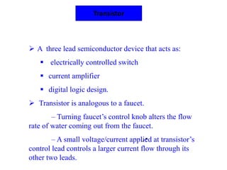
- 1. Transistor A three lead semiconductor device that acts as: electrically controlled switch current amplifier digital logic design. Transistor is analogous to a faucet. – Turning faucet’s control knob alters the flow rate of water coming out from the faucet. – A small voltage/current applied at transistor’s control lead controls a larger current flow through its other two leads.
- 3. Transistor Types Bipolar Junction Transistor (BJT) – NPN and PNP Field Effect Transistor (JFET) – N-channel and P-channel Metal Oxide Semiconductor FET (MOSFET) – Depletion type (n- and p-channel) – Enhancement type (n- and p-channel)
- 4. BJT Structure The BJT has three regions called the emitter, base, and collector. Between the regions are junctions as indicated. B (base) C(collector) n p n Base-Collector junction Base-Emitter junction E (emitter) B C p n E p npn pnp The base is a thin lightly doped region compared to the heavily doped emitter and moderately doped collector regions. The BJT is constructed with three doped semiconductors region separated by two PN junctions.
- 5. NPN PNP NPN: a small input current and a positive voltage applied @ its base (with VB>VE) allows a large current to flow from collector to emitter PNP: a small output current and a negative voltage @ its base (with VB<VE) allows a much larger current to flow from emitter to collector. BJT Types
- 7. BJT Water Analogy NPN (VB > VE)
- 8. BJT Water Analogy PNP (VB < VE)
- 9. BJT Operation In normal operation, the base-emitter is forward-biased and the base-collector is reverse-biased. npn For the pnp type, the voltages are reversed to maintain the forward-reverse bias. – + – + – + + BCreverse- biased – BE forward- biased – + + – – BCreverse- biased + BE forward- biased – + pnp For the npn type shown, the collector is more positive than the base, which is more positive than the emitter.
- 11. BJT Currents IE IE IC IB IC IB n p n p n p + – + – – + IE IC IB + – + IE IC IB + – – npn pnp The direction of conventional current is in the direction of the arrow on the emitter terminal. The emitter current is the sum of the collector current and the small base current. That is, IE = IC + IB.
- 12. Beta The common-emitter current gain is defined as a beta and it is the ratio of collector current to base current. It is represented by βDC . It is the ratio of a dc collector current (IC) to the corresponding dc base current (IB) and it is represented by βDC =IC / IB
- 13. The ratio of the dc collector current (IC) to the dc emitter current (IE) is the dc alpha (α DC ) (αDC )= IC / IE
- 14. BJT Regions of Operation Bipolar Junction transistors have the ability to operate within three different regions: 1. Active Region - the transistor operates as an amplifier and Ic = β.Ib 2. Saturation - the transistor is "fully-ON" operating as a switch and Ic = I(saturation) 3. Cut-off - the transistor is "fully-OFF" operating as a switch and Ic = 0
- 15. BJT Regions of Operation The first region is called cutoff. This is the case where the transistor is essentially inactive. In cutoff, the following behavior is noted: IB = 0 (no base current) Ic = 0 (no collector current) VBE < 0:7V (emitter-base junction is not forward biased) . Whenever we observe the terminals of a BJT and see that the emitter-base junction is not at least 0.6-0.7 volts or base lead open, the transistor is in the cutoff region. In cutoff, the transistor appears as an open circuit between the collector and emitter terminals. IB =0 – + – + ICEO RC VCC VCE ≅VCC RB
- 16. Cutoff In a BJT, cutoff is the condition in which there is no base current, which results in only an extremely small leakage current (ICEO) in the collector circuit. For practical work, this current is assumed to be zero. IB =0 – + – + ICEO RC VCC VCE ≅VCC RB In cutoff, neither the base- emitter junction, nor the base- collector junction are forward- biased. Both base-emitter junction and base-collector junction are reverse -biased
- 17. Saturation The second region is called saturation. In saturation, the following behavior is noted: VCE 0<0.2V ; In this case, VCE assumes the value VCE(sat) IB > 0; and IC > 0 VBE 0 >0.7V Saturation is where the base current has increased well beyond the point that the emitter-base junction is forward biased. In fact, the base current has increased beyond the point where it can cause the collector current flow to increase. In saturation, the transistor appears as a near short circuit between the collector and emitter terminals.
- 18. Saturation In a BJT, saturation is the condition in which there is maximum collector current. The saturation current is determined by the external circuit (VCC and RC in this case) because the collector-emitter voltage is minimum (≈ 0.2 V) In saturation, an increase of base current has no effect on the collector circuit and the relation IC = bDCIB is no longer valid. – + – + VCC VBB VCE = VCC – IC RC RB RC IB IC – + – +
- 19. Active Region The final region of operation of the BJT is the forward active region. It is in this region that the transistor can act as a fairly linear amplifier. In this region: 0:2 < VCE < Vcc ; where Vcc is the supply voltage IB > 0, and Ic > 0 VBE 0:7V
- 20. The collector characteristic curves show the relationship of the three transistor currents. The curve shown is for a fixed based current. The first region is the saturation region. BJT Characteristics IC B C A 0 0.7 V VCE(max) VCE Saturation region Active region Breakdown region As VCE is increased, IC increases until B. Then it flattens in region between points B and C, which is the active region. After C, is the breakdown region.
- 21. Active Region • Transistor is on and the collector to emitter voltage is somewhere between the cutoff and saturated states. • In this state, the transistor is able to amplify small variations in the voltage present on the base. The output is extracted at the collector. • In the forward active state, the collector current is proportional to the base current by a constant multiplier called beta, denoted by the symbol β Thus, in the forward active region we will also observe that: Ic = β*Ib
- 22. The collector characteristic curves illustrate the relationship of the three transistor currents. 0 IC VCE IB6 IB5 IB4 IB3 IB2 IB1 IB = 0 Cutoff region By setting up other values of base current, a family of collector curves is developed. bDC is the ratio of collector current to base current. BJT Characteristics It can be read from the curves. The value of bDC is nearly the same wherever it is read. C DC B I I b
- 23. What is the bDC for the transistor shown? Choose a base current near the center of the range – in this case IB3 which is 30 mA. IC VCE IB6 IB5 IB4 B3 I IB2 B1 I IB = 0 = 10 A m = 20 A m = 30 A m = 0 = 60 A m = 40 A m = 50 A m 10.0 8.0 6.0 4.0 2.0 0 (mA) Read the corresponding collector current – in this case, 5.0 mA. Calculate the ratio: C DC B 5.0 mA 30 A I I b m 167 BJT Characteristics
- 24. DC Load Line the transistor. It is drawn by connecting the saturation and cutoff points. The transistor characteristic curves are shown superimposed on the load line. The region between the saturation and cutoff points is called the active region. The DC load line represents the circuit that is external to 0 IC VCE IB =0 Cutoff VCE(sat) VCC IC(sat) Saturation
- 25. DC and AC Quantities The text uses capital letters for both AC and DC currents and voltages with rms values assumed unless stated otherwise. DC Quantities use upper case roman subscripts. Example: VCE. (The second letter in the subscript indicates the reference point.) AC Quantities and time varying signals use lower case italic subscripts. Example: Vce. Internal transistor resistances are indicated as lower case quantities with a prime and an appropriate subscript. Example: re ’. External resistances are indicated as capital R with either a capital or lower case subscript depending on if it is a DC or ac resistance. Examples: RC and Rc.