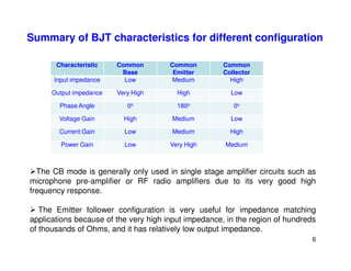
Download to read offline


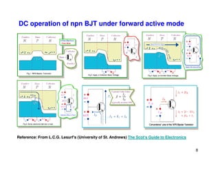
![1 2
3
4
E-field
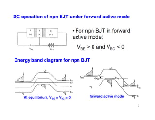
DC operation of npn BJT under forward active mode
1 . Forward bias of EBJ causes electrons to diffuse from emitter into base.
2. As base region is very thin, the majority of these electrons diffuse to the
edge of the depletion region of CBJ, and then are swept to the collector by the
electric field of the reverse-biased CBJ.
3. A small fraction of these electrons recombine with the holes in base region.
4. Holes are injected from base to emitter region. (4) (1).
9
The two-carrier flow from [(1) and (4)] forms the emitter current (IE).](https://image.slidesharecdn.com/lec-5-221021173633-93304083/85/Lec-5-pdf-9-320.jpg)

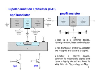
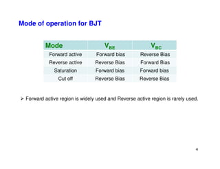
This document discusses the bipolar junction transistor (BJT). It begins by introducing the BJT as one of the most popular semiconductor devices besides diodes. It then discusses key applications of transistors as amplifiers, oscillators, and switches. The document goes on to describe the structure and doping of NPN and PNP BJT devices. It also covers the different configurations (common base, common emitter, common collector) and their characteristics. The document concludes by explaining the DC operation and forward active mode of an NPN BJT through band diagrams and equations.