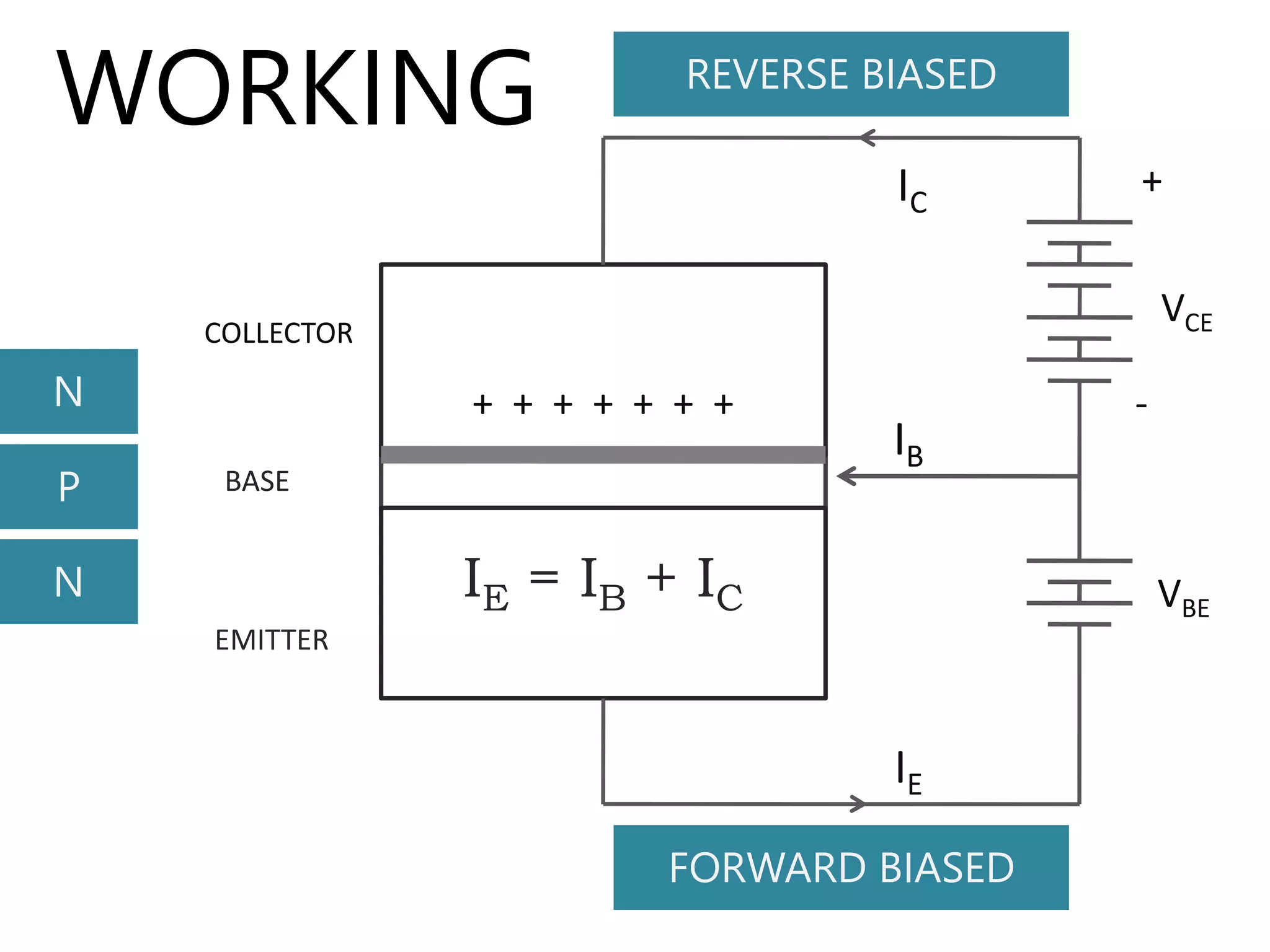
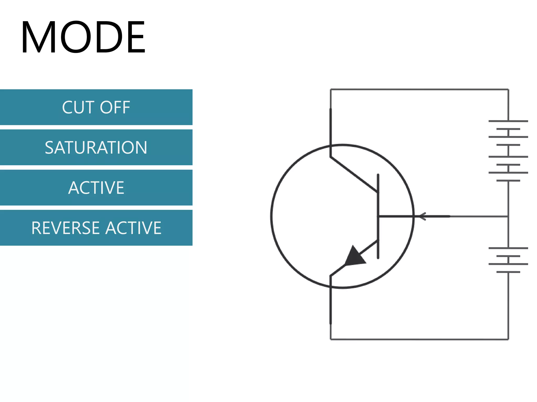
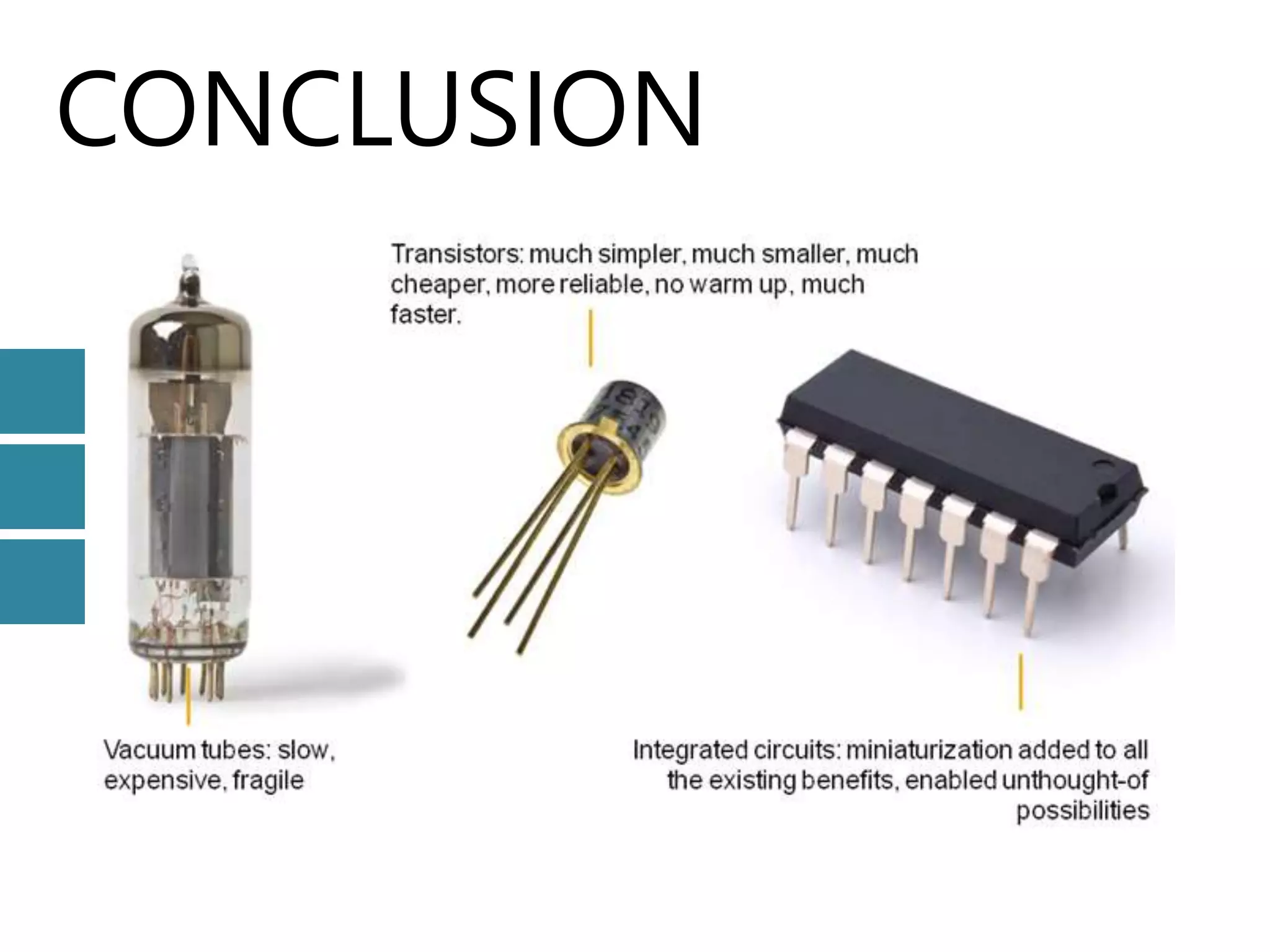
BIPOLAR JUNCTION
TRANSISTOR
THAISA JAWHLY
UNDER THE SUPERVISION OF
DR. R.C TIWARI
SCHOOL OF PHYSICAL SCIENCE
MIZORAM UNIVERSITY
TANHRIL
TRANSISTOR
IMPORTANT INVENTION OF THE
20TH CENTURY
BARDEEN , BRATTAIN &
SHOCKLEY 1947 – BELL LABS
AMPLIFY , SWITCH ELECTRONIC
DEVICES
BASE
CONSTRUCTION
P
P
N
COLLECTOR
EMITTER
PNP TRANSISTOR
LIGHTLY DOPED
HEAVILY DOPED
HEAVILY DOPED
BASE
CONSTRUCTION
N
N
P
COLLECTOR
EMITTER
NPN TRANSISTOR
WORKING
N
N
P
COLLECTOR
BASE
EMITTER
VCE
+
-
VBE
+ + + + + + +
FORWARD BIASED
REVERSE BIASED
WORKING
N
N
P
COLLECTOR
BASE
EMITTER
VCE
+
-
VBE
+ + + + + + +
FORWARD BIASED
REVERSE BIASED
IB
IC
IE
IE = IB + IC
MODE
VCE
+
-
VBE
IB
IC
IE
N
N
P
COLLECTOR
BASE
EMITTER
IE = IB + IC
MODE
CUT OFF
SATURATION
ACTIVE
REVERSE ACTIVE
MODE
CUT OFF
SATURATION
ACTIVE
REVERSE ACTIVE
SWITCH
N
N
P
AMPLIFIER
N
N
P
CONFIGURATION
COMMON
BASE
COMMON
EMITTER
COMMON
COLLECTOR
TRANSISTOR CONFIGURATION SUMMARY TABLE
TRANSISTOR CONFIGURATION COMMON BASE COMMON
COLLECTOR
(EMITTER
FOLLOWER)
COMMON EMITTER
Voltage gain High Low Medium
Current gain Low High Medium
Power gain Low Medium High
Input / output phase relationship 0° 0° 180°
Input resistance Low High Medium
Output resistance High Low Medium
CONCLUSION
REFERENCES
Kittel, C., Introduction to Solid State Physics, 6th
Ed., New York:John Wiley,
http://www.aps.org/publications/apsnews/200011
/history.cfm
http://www.radio-
electronics.com/info/data/semicond/bipolar-
transistor-bjt/operation-how-transistor-works.php
https://learn.sparkfun.com/tutorials/transistors/op
eration-modes
http://www.electronics-
tutorials.ws/transistor/tran10.gif?81223b
http://www.electronics-
tutorials.ws/transistor/tran12.gif
THANK YOU

Bipolar junction transistor

Editor's Notes

  • #3 Transistor is considered one of the most important invention of the 20th century replacing the vaccum tubes. Invented at the Bell Labs, United state by John Bardeen, Wesley Brattain and William Shockley in 1947 a transistor is used to amplify signals and acts as a switch in electronic devices
  • #4 It consists of a lightly doped n type material called the Base which is sandwiched between two heavily doped P type material. Upper p type material is made physically larger so as to handle a large amount of current and this constitutes the collector. The lower semiconductor material constitutes the emitter. This is the basic construction of a pnp type transistor which is usually represented by a round symbol consisting of three terminals with an arrow pointing towards the base in the emitter section signifying that it is a pnp type transistor
  • #5  Similarly we can have an NPN type transistor as shown in the illustration. In this case the p type material is sandwiched between two N-type material. This is again represented by the round symbol consisting of three terminals with an arrow pointing out of the base in the emitter section signifying that it is an npn-type transistor