
Downloaded 65 times

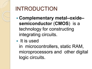
![ The words "complementary-
symmetry" refer to the fact that
the typical digital design style with
CMOS uses complementary and
symmetrical pairs of p-type and n-
type metal oxide semiconductor
field effect
transistors (MOSFETs) for logic
functions.[2]](https://image.slidesharecdn.com/bjtandcmosasaswitch-150405123624-conversion-gate01/85/Bjt-and-cmos-as-a-switch-11-320.jpg)
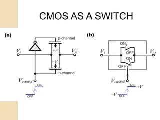
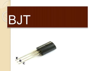
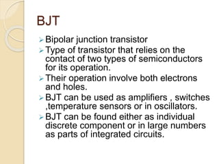
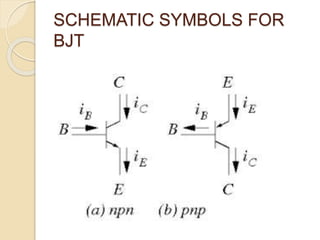
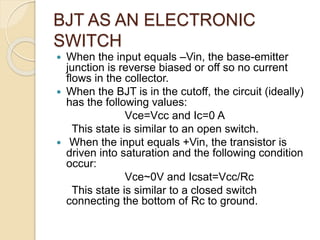
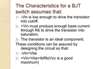
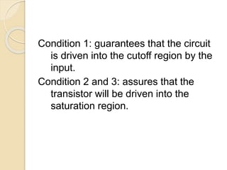
The document discusses Bipolar Junction Transistors (BJT) and CMOS as electronic switches. BJTs can be used as switches by utilizing the cutoff and saturation regions of operation. When in cutoff, the BJT is off and no current flows. When in saturation, it is on and connects the bottom of a resistor to ground. CMOS circuits use complementary pairs of PMOS and NMOS transistors for logic functions. As a switch, applying a low voltage turns on the PMOS and off the NMOS, connecting the output to the voltage source. A high voltage turns on the NMOS and off the PMOS, connecting the output to ground.


![Chp1 1 bjt [read only]](https://cdn.slidesharecdn.com/ss_thumbnails/chp11bjtread-only-130929091550-phpapp02-thumbnail.jpg?width=640&height=640&fit=bounds)


