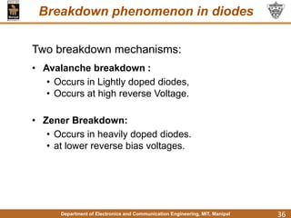
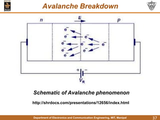
1) The document discusses diodes and their applications, covering topics like PN junction diodes, I-V characteristics, breakdown mechanisms, equivalent circuits, and Zener diodes.
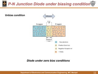
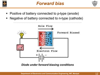
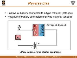
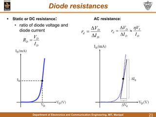
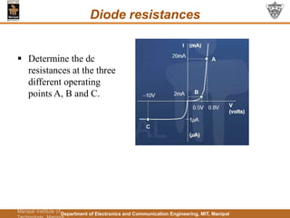
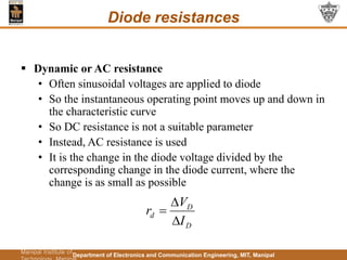
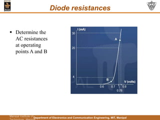
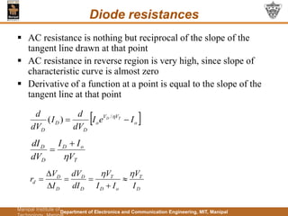
2) It describes the operation of PN junction diodes under different biasing conditions and their static and dynamic resistances.
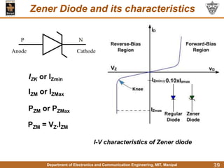
3) Zener diodes exhibit a constant voltage breakdown characteristic and are used to regulate voltage in applications like power supplies.
![Department of Electronics and Communication Engineering, MIT, Manipal
Doping in Semiconductors
6
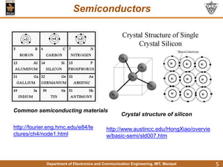
Schematic of a silicon crystal lattice doped with impurities to
produce n-type and p-type semiconductor material.
[http://www.pveducation.org/pvcdrom/pn-junction/dopingl].](https://image.slidesharecdn.com/module1diode-240312060423-a85616a0/85/Basic-engineering-electronics-Module-1_Diode-ppt-6-320.jpg)
![Department of Electronics and Communication Engineering, MIT, Manipal
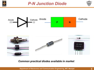
P-N Junction Diode under biasing
10
P-N junction (a) in contact (b) formation of depletion region
[http://www.imagesco.com/articles/photovoltaic/photovoltaic-pg3.html].](https://image.slidesharecdn.com/module1diode-240312060423-a85616a0/85/Basic-engineering-electronics-Module-1_Diode-ppt-10-320.jpg)

![Department of Electronics and Communication Engineering, MIT, Manipal
Ideal diode : I-V characteristics
29
I-V characteristic of Ideal diode and ideal models
[http://conceptselectronics.com/diodes/diode-equivalent-models/].](https://image.slidesharecdn.com/module1diode-240312060423-a85616a0/85/Basic-engineering-electronics-Module-1_Diode-ppt-29-320.jpg)