EC24101 BE Module 3 basic electronic by birla .pdf
1.
EE24101 Basic Electronics
Module3: Field Effect Transistors
Dr. Jyoti Sharma
BIT Mesra, Jaipur Campus
November 8, 2025
Dr. Jyoti Sharma (BIT Mesra, Jaipur Campus) EE24101 Basic Electronics November 8, 2025 1 / 85
2.
Overview
1 Introduction
2 JFET:Principle of operation, transfer characteristics
3 MOSFET: Operation of NMOS, PMOS, enhancement and depletion
type, transfer characteristics
4 CS biasing of JFET and MOSFET
Dr. Jyoti Sharma (BIT Mesra, Jaipur Campus) EE24101 Basic Electronics November 8, 2025 2 / 85
3.
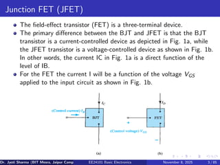
Junction FET (JFET)
Thefield-effect transistor (FET) is a three-terminal device.
The primary difference between the BJT and JFET is that the BJT
transistor is a current-controlled device as depicted in Fig. 1a, while
the JFET transistor is a voltage-controlled device as shown in Fig. 1b.
In other words, the current IC in Fig. 1a is a direct function of the
level of IB.
For the FET the current I will be a function of the voltage VGS
applied to the input circuit as shown in Fig. 1b.
Dr. Jyoti Sharma (BIT Mesra, Jaipur Campus) EE24101 Basic Electronics November 8, 2025 3 / 85
4.
Junction FET (JFET)
Justas there are npn and pnp bipolar transistors, there are n-channel
and p-channel field-effect transistors.
However, it is important to keep in mind that the BJT transistor is a
bipolar device—the prefix bi- revealing that the conduction level is a
function of two charge carriers, electrons and holes.
The FET is a unipolar device depending solely on either electron
(n-channel) or hole (p-channel) conduction.
The term field-effect in the chosen name is due to an electric field
established by the charges present that will control the conduction
path of the output circuit without the need for direct contact between
the controlling and controlled quantities.
Dr. Jyoti Sharma (BIT Mesra, Jaipur Campus) EE24101 Basic Electronics November 8, 2025 4 / 85
5.
Characteristics of JFET:
•high input impedance
• FETs are more temperature stable than BJTs
• FETs are usually smaller in construction than BJTs, making them
particularly useful in integrated-circuit (IC) chips.
Two types of FETs:
• the junction field-effect transistor (JFET) and
• the metal-oxide-semiconductor field-effect transistor (MOSFET).
The MOSFET category is further broken down into:
• depletion type MOSFET and
• enhancement type MOSFET
Dr. Jyoti Sharma (BIT Mesra, Jaipur Campus) EE24101 Basic Electronics November 8, 2025 5 / 85
6.
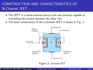
CONSTRUCTION AND CHARACTERISTICSOF
N-Channel JFET
The JFET is a three-terminal device with one terminal capable of
controlling the current between the other two.
The basic construction of the n-channel JFET is shown in Fig. 2.
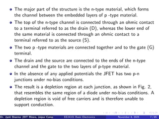
Figure 2: Junction FET
Dr. Jyoti Sharma (BIT Mesra, Jaipur Campus) EE24101 Basic Electronics November 8, 2025 6 / 85
7.
The major partof the structure is the n-type material, which forms
the channel between the embedded layers of p -type material.
The top of the n-type channel is connected through an ohmic contact
to a terminal referred to as the drain (D), whereas the lower end of
the same material is connected through an ohmic contact to a
terminal referred to as the source (S).
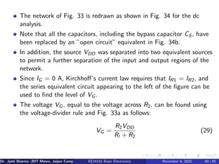
The two p -type materials are connected together and to the gate (G)
terminal.
The drain and the source are connected to the ends of the n-type
channel and the gate to the two layers of p-type material.
In the absence of any applied potentials the JFET has two p-n
junctions under no-bias conditions.
The result is a depletion region at each junction, as shown in Fig. 2,
that resembles the same region of a diode under no-bias conditions. A
depletion region is void of free carriers and is therefore unable to
support conduction.
Dr. Jyoti Sharma (BIT Mesra, Jaipur Campus) EE24101 Basic Electronics November 8, 2025 7 / 85
8.
VGS= 0 V,VDS= Some Positive Value
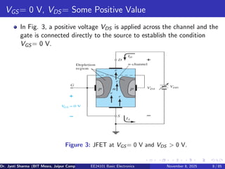
In Fig. 3, a positive voltage VDS is applied across the channel and the
gate is connected directly to the source to establish the condition
VGS = 0 V.
Figure 3: JFET at VGS = 0 V and VDS > 0 V.
Dr. Jyoti Sharma (BIT Mesra, Jaipur Campus) EE24101 Basic Electronics November 8, 2025 8 / 85
9.
The result isa gate and a source terminal at the same potential and a
depletion region in the low end of each p-material similar to the
distribution of the no-bias conditions of Fig. 2.
The instant the voltage VDD (=VDS ) is applied, the electrons are
drawn to the drain terminal, establishing the conventional current ID
with the defined direction of Fig. 3.
The path of charge flow clearly reveals that the drain and source
currents are equivalent (ID = IS ).
Under the conditions in Fig. 3, the flow of charge is relatively
uninhibited and is limited solely by the resistance of the n-channel
between drain and source.
Dr. Jyoti Sharma (BIT Mesra, Jaipur Campus) EE24101 Basic Electronics November 8, 2025 9 / 85
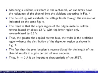
10.
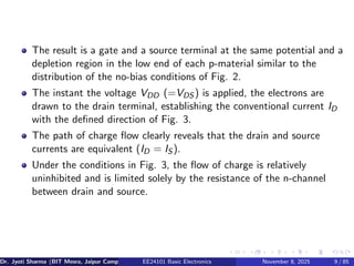
The depletion regionis wider near the top of both p-type materials.
The reason for the change in width of the region is explained with the
help of Fig. 4.
Figure 4: Varying reverse-bias potentials across the p–n junction of an n-chann
JFET.
Dr. Jyoti Sharma (BIT Mesra, Jaipur Campus) EE24101 Basic Electronics November 8, 2025 10 / 85
11.
Assuming a uniformresistance in the n-channel, we can break down
the resistance of the channel into the divisions appearing in Fig. 4.
The current ID will establish the voltage levels through the channel as
indicated on the same figure.
The result is that the upper region of the p-type material will be
reverse-biased by about 1.5 V, with the lower region only
reverse-biased by 0.5 V.
Thus, the greater the applied reverse bias, the wider is the depletion
region—hence the distribution of the depletion region as shown in
Fig. 4.
The fact that the p–n junction is reverse-biased for the length of the
channel results in a gate current of zero amperes.
Thus, IG = 0 A is an important characteristic of the JFET.
Dr. Jyoti Sharma (BIT Mesra, Jaipur Campus) EE24101 Basic Electronics November 8, 2025 11 / 85
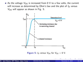
12.
As the voltageVDS is increased from 0 V to a few volts, the current
will increase as determined by Ohm’s law and the plot of ID versus
VDS will appear as shown in Fig. 5.
Figure 5: ID versus VDS for VGS = 0 V.
Dr. Jyoti Sharma (BIT Mesra, Jaipur Campus) EE24101 Basic Electronics November 8, 2025 12 / 85
13.
The relative straightnessof the plot reveals that for the region of low
values of VDS , the resistance is essentially constant.
As VDS increases and approaches a level referred to as VP in Fig. 5,
the depletion regions of Fig. 3 will widen, causing a noticeable
reduction in the channel width.
The reduced path of conduction causes the resistance to increase and
the curve in the graph of Fig. 5 to occur.
The more horizontal the curve, the higher the resistance, suggesting
that the resistance is approaching ”infinite” ohms in the horizontal
region.
Dr. Jyoti Sharma (BIT Mesra, Jaipur Campus) EE24101 Basic Electronics November 8, 2025 13 / 85
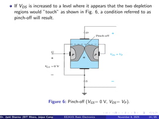
14.
If VDS isincreased to a level where it appears that the two depletion
regions would ”touch” as shown in Fig. 6, a condition referred to as
pinch-off will result.
Figure 6: Pinch-off (VGS = 0 V, VDS = VP ).
Dr. Jyoti Sharma (BIT Mesra, Jaipur Campus) EE24101 Basic Electronics November 8, 2025 14 / 85
15.
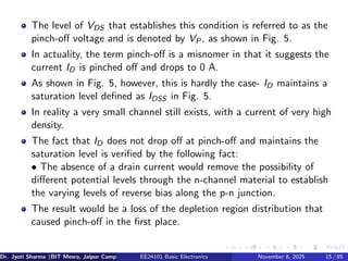
The level ofVDS that establishes this condition is referred to as the
pinch-off voltage and is denoted by VP, as shown in Fig. 5.
In actuality, the term pinch-off is a misnomer in that it suggests the
current ID is pinched off and drops to 0 A.
As shown in Fig. 5, however, this is hardly the case- ID maintains a
saturation level defined as IDSS in Fig. 5.
In reality a very small channel still exists, with a current of very high
density.
The fact that ID does not drop off at pinch-off and maintains the
saturation level is verified by the following fact:
• The absence of a drain current would remove the possibility of
different potential levels through the n-channel material to establish
the varying levels of reverse bias along the p-n junction.
The result would be a loss of the depletion region distribution that
caused pinch-off in the first place.
Dr. Jyoti Sharma (BIT Mesra, Jaipur Campus) EE24101 Basic Electronics November 8, 2025 15 / 85
16.
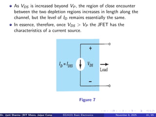
As VDS isincreased beyond VP, the region of close encounter
between the two depletion regions increases in length along the
channel, but the level of ID remains essentially the same.
In essence, therefore, once VDS > VP the JFET has the
characteristics of a current source.
Figure 7
Dr. Jyoti Sharma (BIT Mesra, Jaipur Campus) EE24101 Basic Electronics November 8, 2025 16 / 85
17.
As shown inFig. 7, the current is fixed at ID = IDSS , but the voltage
VDS (for levels > VP) is determined by the applied load.
The choice of notation IDSS is derived from the fact that it is the
drain-to-source current with a short-circuit connection from gate to
source.
As we continue to investigate the characteristics of the device we will
find that:
• IDSS is the maximum drain current for a JFET and is defined
by the conditions VGS = 0 V and VDS > |VP|.
Dr. Jyoti Sharma (BIT Mesra, Jaipur Campus) EE24101 Basic Electronics November 8, 2025 17 / 85
18.
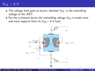
VGS < 0V
The voltage from gate to source, denoted VGS , is the controlling
voltage of the JFET.
For the n-channel device the controlling voltage VGS is made more
and more negative from its VGS = 0 V level.
Dr. Jyoti Sharma (BIT Mesra, Jaipur Campus) EE24101 Basic Electronics November 8, 2025 18 / 85
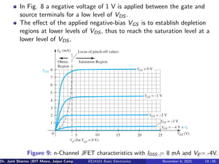
19.
In Fig. 8a negative voltage of 1 V is applied between the gate and
source terminals for a low level of VDS .
The effect of the applied negative-bias VGS is to establish depletion
regions at lower levels of VDS , thus to reach the saturation level at a
lower level of VDS ,
Figure 9: n-Channel JFET characteristics with IDSS = 8 mA and VP = -4V.
Dr. Jyoti Sharma (BIT Mesra, Jaipur Campus) EE24101 Basic Electronics November 8, 2025 19 / 85
20.
The resulting saturationlevel for ID has been reduced and in fact will
continue to decrease as VGS is made more and more negative.
The pinch-off voltage continues to drop in a parabolic manner as VGS
becomes more and more negative.
Eventually, VGS when VGS =−VP will be sufficiently negative to
establish a saturation level that is essentially 0 mA, and for all
practical purposes the device has been ”turned off”.
In summary: The level of VGS that results in ID= 0 mA is defined by
VGS = VP, with VP being a negative voltage for n-channel devices
and a positive voltage for p-channel JFETs.
Dr. Jyoti Sharma (BIT Mesra, Jaipur Campus) EE24101 Basic Electronics November 8, 2025 20 / 85
21.
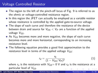
Voltage Controlled Resistor
Theregion to the left of the pinch-off locus of Fig. 9 is referred to as
the ohmic or voltage-controlled resistance region.
In this region the JFET can actually be employed as a variable resistor
whose resistance is controlled by the applied gate-to-source voltage.
The slope of each curve and therefore the resistance of the device
between drain and source for VDS < VP are a function of the applied
voltage VGS .
As VGS becomes more and more negative, the slope of each curve
becomes more and more horizontal, corresponding to an increasing
resistance level.
The following equation provides a good first approximation to the
resistance level in terms of the applied voltage VGS :
rd =
r0
(1 − VGS /VP)2
(1)
where ro is the resistance with VGS = 0 V and rd is the resistance at a
particular level of VGS .
Dr. Jyoti Sharma (BIT Mesra, Jaipur Campus) EE24101 Basic Electronics November 8, 2025 21 / 85
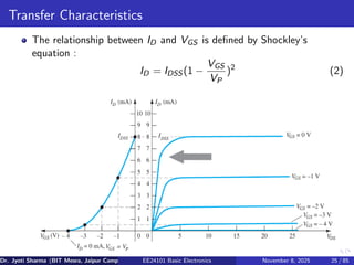
Transfer Characteristics
The relationshipbetween ID and VGS is defined by Shockley’s
equation :
ID = IDSS (1 −
VGS
VP
)2
(2)
Dr. Jyoti Sharma (BIT Mesra, Jaipur Campus) EE24101 Basic Electronics November 8, 2025 25 / 85
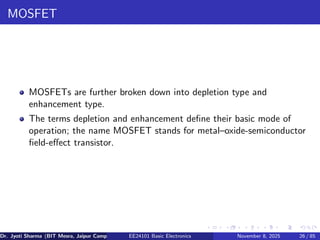
26.
MOSFET
MOSFETs are furtherbroken down into depletion type and
enhancement type.
The terms depletion and enhancement define their basic mode of
operation; the name MOSFET stands for metal–oxide-semiconductor
field-effect transistor.
Dr. Jyoti Sharma (BIT Mesra, Jaipur Campus) EE24101 Basic Electronics November 8, 2025 26 / 85
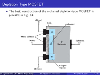
27.
Depletion Type MOSFET
Thebasic construction of the n-channel depletion-type MOSFET is
provided in Fig. 14.
Dr. Jyoti Sharma (BIT Mesra, Jaipur Campus) EE24101 Basic Electronics November 8, 2025 27 / 85
28.
A slab ofp-type material is formed from a silicon base and is referred
to as the substrate.
In some cases the substrate is internally connected to the source
terminal.
However, many discrete devices provide an additional terminal labeled
SS, resulting in a four-terminal device.
The source and drain terminals are connected through metallic
contacts to n-doped regions linked by an n-channel as shown in the
figure.
The gate is also connected to a metal contact surface but remains
insulated from the n-channel by a very thin silicon dioxide (SiO2)
layer.
SiO2 is a type of insulator referred to as a dielectric, which sets up
opposing electric fields within the dielectric when exposed to an
externally applied field.
Dr. Jyoti Sharma (BIT Mesra, Jaipur Campus) EE24101 Basic Electronics November 8, 2025 28 / 85
29.
The fact thatthe SiO2 layer is an insulating layer means that:
• There is no direct electrical connection between the gate
terminal and the channel of a MOSFET.
It is the insulating layer of SiO2 in the MOSFET construction that
accounts for the very desirable high input impedance of the device.
The reason for the label metal–oxide–semiconductor FET is: metal
for the drain, source, and gate connections; oxide for the silicon
dioxide insulating layer; and semiconductor for the basic structure on
which the n- and p-type regions are diffused.
The insulating layer between the gate and the channel has resulted in
another name for the device: insulated-gate FET, or IGFET.
Dr. Jyoti Sharma (BIT Mesra, Jaipur Campus) EE24101 Basic Electronics November 8, 2025 29 / 85
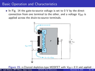
30.
Basic Operation andCharacteristics
In Fig. 14 the gate-to-source voltage is set to 0 V by the direct
connection from one terminal to the other, and a voltage VDD is
applied across the drain-to-source terminals.
Figure 15: n-Channel depletion-type MOSFET with VGS = 0 V and applied
Dr. Jyoti Sharma (BIT Mesra, Jaipur Campus) EE24101 Basic Electronics November 8, 2025 30 / 85
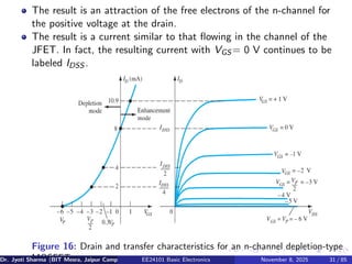
31.
The result isan attraction of the free electrons of the n-channel for
the positive voltage at the drain.
The result is a current similar to that flowing in the channel of the
JFET. In fact, the resulting current with VGS = 0 V continues to be
labeled IDSS .
Figure 16: Drain and transfer characteristics for an n-channel depletion-type
MOSFET.
Dr. Jyoti Sharma (BIT Mesra, Jaipur Campus) EE24101 Basic Electronics November 8, 2025 31 / 85
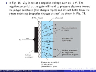
32.
In Fig. 15,VGS is set at a negative voltage such as -1 V. The
negative potential at the gate will tend to pressure electrons toward
the p-type substrate (like charges repel) and attract holes from the
p-type substrate (opposite charges attract) as shown in Fig. ??.
Dr. Jyoti Sharma (BIT Mesra, Jaipur Campus) EE24101 Basic Electronics November 8, 2025 32 / 85
33.
Depending on theand holes will occur that will reduce the number of
free electrons in the n -channel available for conduction.
The more negative the bias, the higher is the rate of recombination.
The resulting level of drain current is therefore reduced with
increasing negative bias for VGS , as shown in Fig. for VGS =-1 V, -2
V, and so on, to the pinch-off level of -6 V.
For positive values of VGS , the positive gate will draw additional
electrons (free carriers) from the p-type substrate due to the reverse
leakage current and establish new carriers through the collisions
resulting between accelerating particles.
As the gate-to-source voltage continues to increase in the positive
direction, Fig. 16 reveals that the drain current will increase at a
rapid rate for the reasons listed above.
Dr. Jyoti Sharma (BIT Mesra, Jaipur Campus) EE24101 Basic Electronics November 8, 2025 33 / 85
34.
The vertical spacingbetween the VGS = 0 V and VGS = +1 V curves
of Fig. 16 is a clear indication of how much the current has increased
for the 1-V change in VGS .
Due to the rapid rise, the user must be aware of the maximum drain
current rating since it could be exceeded with a positive gate voltage.
As revealed above, the application of a positive gate-to-source voltage
has “enhanced” the level of free carriers in the channel compared to
that encountered 0 V.
For this reason the region of positive gate voltages on the drain or
transfer with VGS characteristics is often referred to as the
enhancement region, with the region between cutoff and the
saturation level of IDSS referred to as the depletion region.
Dr. Jyoti Sharma (BIT Mesra, Jaipur Campus) EE24101 Basic Electronics November 8, 2025 34 / 85
35.
p-Channel Depletion-Type MOSFET
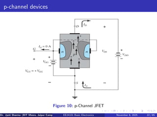
Theconstruction of a p-channel depletion-type MOSFET is exactly
the reverse of that appearing in Fig. 15.
That is, there is now an n-type substrate and a p-type channel, as
shown in Fig. 18. The terminals remain as identified, but all the
voltage polarities and the current directions are reversed, as shown in
the same figure.
Dr. Jyoti Sharma (BIT Mesra, Jaipur Campus) EE24101 Basic Electronics November 8, 2025 35 / 85
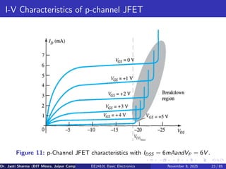
36.
p-Channel Depletion-Type MOSFET
Thedrain characteristics would appear exactly as in Fig. 16, but with
VDS having negative values, ID having positive values as indicated
(since the defined direction is now reversed), and VGS having the
opposite polarities as shown in Fig. 18b.
The reversal in VGS will result in a mirror image (about the ID axis)
for the transfer characteristics as shown in Fig. 18b. In other words,
the drain current will increase from cutoff at VGS = VP in the
positive VGS region to IDSS and then continue to increase for
increasingly negative values of VGS .
Shockley’s equation is still applicable and requires simply placing the
correct sign for both VGS and VP in the equation.
Dr. Jyoti Sharma (BIT Mesra, Jaipur Campus) EE24101 Basic Electronics November 8, 2025 36 / 85
37.
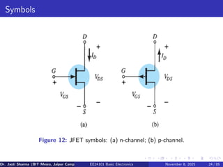
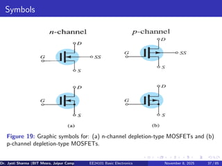
Symbols
Figure 19: Graphicsymbols for: (a) n-channel depletion-type MOSFETs and (b)
p-channel depletion-type MOSFETs.
Dr. Jyoti Sharma (BIT Mesra, Jaipur Campus) EE24101 Basic Electronics November 8, 2025 37 / 85
38.
Enhancement MOSFET
The basicconstruction of the n-channel enhancement-type MOSFET
is provided in Fig. 20.
Figure 20
Dr. Jyoti Sharma (BIT Mesra, Jaipur Campus) EE24101 Basic Electronics November 8, 2025 38 / 85
39.
Enhancement MOSFET
A slabof p-type material is formed from a silicon base and is again
referred to as the substrate.
As with the depletion-type MOSFET, the substrate is sometimes
internally connected to the source terminal, whereas in other cases a
fourth lead (labeled SS) is made available for external control of its
potential level.
The source and drain terminals are again connected through metallic
contacts to n-doped regions, but note in Fig. 20 the absence of a
channel between the two n-doped regions.
This is the primary difference between the construction of
depletion-type and enhancement-type MOSFETs—the absence of a
channel as a constructed component of the device.
The Si O2 layer is still present to isolate the gate metallic platform
from the region between the drain and source, but now it is simply
separated from a section of the p-type material.
Dr. Jyoti Sharma (BIT Mesra, Jaipur Campus) EE24101 Basic Electronics November 8, 2025 39 / 85
40.
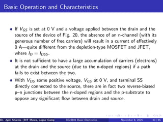
Basic Operation andCharacteristics
If VGS is set at 0 V and a voltage applied between the drain and the
source of the device of Fig. 20, the absence of an n-channel (with its
generous number of free carriers) will result in a current of effectively
0 A—quite different from the depletion-type MOSFET and JFET,
where ID = IDSS .
It is not sufficient to have a large accumulation of carriers (electrons)
at the drain and the source (due to the n-doped regions) if a path
fails to exist between the two.
With VDS some positive voltage, VGS at 0 V, and terminal SS
directly connected to the source, there are in fact two reverse-biased
p–n junctions between the n-doped regions and the p-substrate to
oppose any significant flow between drain and source.
Dr. Jyoti Sharma (BIT Mesra, Jaipur Campus) EE24101 Basic Electronics November 8, 2025 40 / 85
41.
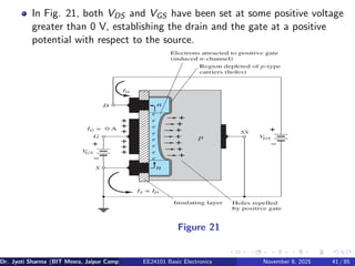
In Fig. 21,both VDS and VGS have been set at some positive voltage
greater than 0 V, establishing the drain and the gate at a positive
potential with respect to the source.
Figure 21
Dr. Jyoti Sharma (BIT Mesra, Jaipur Campus) EE24101 Basic Electronics November 8, 2025 41 / 85
42.
The positive potentialat the gate will pressure the holes (since like
charges repel) in the p-substrate along the edge of the SiO2 layer to
leave the area and enter deeper regions of the p-substrate, as shown
in the figure.
The result is a depletion region near the SiO2 insulating layer void of
holes.
However, the electrons in the p-substrate (the minority carriers of the
material) will be attracted to the positive gate and accumulate in the
region near the surface of the SiO2 layer.
The SiO2 layer and its insulating qualities will prevent the negative
carriers from being absorbed at the gate terminal.
As VGS increases in magnitude, the concentration of electrons near
the SiO2 surface increases until eventually the induced n-type region
can support a measurable flow between drain and source.
The level of VGS that results in the significant increase in drain
current is called the threshold voltage and is given the symbol VT .
Dr. Jyoti Sharma (BIT Mesra, Jaipur Campus) EE24101 Basic Electronics November 8, 2025 42 / 85
43.
Since the channelis nonexistent with VGS = 0 V and “enhanced” by
the application of a positive gate-to-source voltage, this type of
MOSFET is called an enhancement-type MOSFET.
Both depletion- and enhancement type MOSFETs have
enhancement-type regions, but the label was applied to the latter
since it is its only mode of operation.
As VGS is increased beyond the threshold level, the density of free
carriers in the induced channel will increase, resulting in an increased
level of drain current.
However, if we hold VGS constant and increase the level of VDS , the
drain current will eventually reach a saturation level as occurred for
the JFET and depletion-type MOSFET.
Dr. Jyoti Sharma (BIT Mesra, Jaipur Campus) EE24101 Basic Electronics November 8, 2025 43 / 85
44.
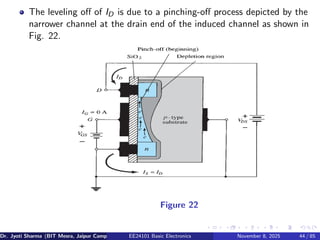
The leveling offof ID is due to a pinching-off process depicted by the
narrower channel at the drain end of the induced channel as shown in
Fig. 22.
Figure 22
Dr. Jyoti Sharma (BIT Mesra, Jaipur Campus) EE24101 Basic Electronics November 8, 2025 44 / 85
45.
Applying Kirchhoff’s voltagelaw to the terminal voltages of the
MOSFET of Fig. 22, we find that
VDG = VDS − VGS (3)
If VGS is held fixed at some value such as 8 V and VDS is increased
from 2 V to 5 V, the voltage VDG [by Eq. 3] will increase from -6 V
to -3 V and the gate will become less and less positive with respect to
the drain.
This reduction in gate-to-drain voltage will in turn reduce the
attractive forces for free carriers (electrons) in this region of the
induced channel, causing a reduction in the effective channel width.
Eventually, the channel will be reduced to the point of pinch-off and a
saturation condition will be established as described earlier for the
JFET and depletion-type MOSFET.
In other words, any further increase in VDS at the fixed value of VGS
will not affect the saturation level of ID until breakdown conditions
are encountered.
Dr. Jyoti Sharma (BIT Mesra, Jaipur Campus) EE24101 Basic Electronics November 8, 2025 45 / 85
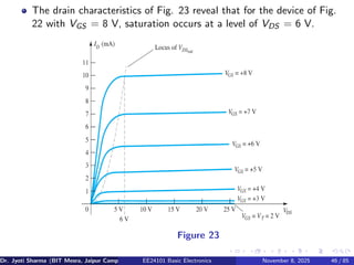
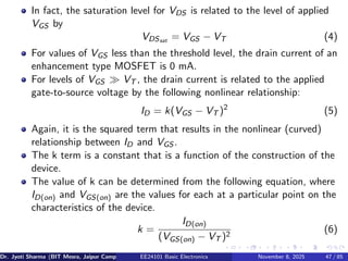
46.
The drain characteristicsof Fig. 23 reveal that for the device of Fig.
22 with VGS = 8 V, saturation occurs at a level of VDS = 6 V.
Figure 23
Dr. Jyoti Sharma (BIT Mesra, Jaipur Campus) EE24101 Basic Electronics November 8, 2025 46 / 85
47.
In fact, thesaturation level for VDS is related to the level of applied
VGS by
VDSsat = VGS − VT (4)
For values of VGS less than the threshold level, the drain current of an
enhancement type MOSFET is 0 mA.
For levels of VGS ≫ VT , the drain current is related to the applied
gate-to-source voltage by the following nonlinear relationship:
ID = k(VGS − VT )2
(5)
Again, it is the squared term that results in the nonlinear (curved)
relationship between ID and VGS .
The k term is a constant that is a function of the construction of the
device.
The value of k can be determined from the following equation, where
ID(on) and VGS(on) are the values for each at a particular point on the
characteristics of the device.
k =
ID(on)
(VGS(on) − VT )2
(6)
Dr. Jyoti Sharma (BIT Mesra, Jaipur Campus) EE24101 Basic Electronics November 8, 2025 47 / 85
48.
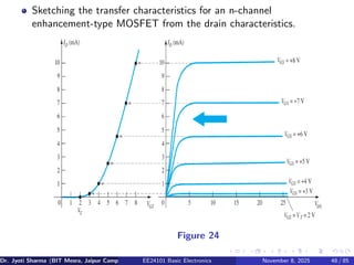
Sketching the transfercharacteristics for an n-channel
enhancement-type MOSFET from the drain characteristics.
Figure 24
Dr. Jyoti Sharma (BIT Mesra, Jaipur Campus) EE24101 Basic Electronics November 8, 2025 48 / 85
49.
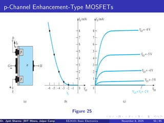
p-Channel Enhancement-Type MOSFETs
Theconstruction of a p-channel enhancement-type MOSFET is
shown in Fig. 25.
There is now an n-type substrate and p-doped regions under the drain
and source connections.
The terminals remain as identified, but all the voltage polarities and
the current directions are reversed.
The drain characteristics will appear as shown in Fig. 25c, with
increasing levels of current resulting from increasingly negative values
of VGS .
The transfer characteristics of Fig. 25b will be the mirror image
(about the ID axis) of the transfer curve of Fig. 24, with ID increasing
with increasingly negative values of VGS beyond VT , as shown in Fig.
25c.
Dr. Jyoti Sharma (BIT Mesra, Jaipur Campus) EE24101 Basic Electronics November 8, 2025 49 / 85
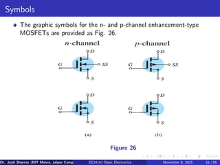
Symbols
The graphic symbolsfor the n- and p-channel enhancement-type
MOSFETs are provided as Fig. 26.
Figure 26
Dr. Jyoti Sharma (BIT Mesra, Jaipur Campus) EE24101 Basic Electronics November 8, 2025 51 / 85
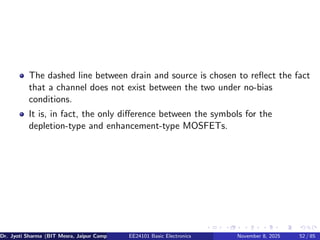
52.
The dashed linebetween drain and source is chosen to reflect the fact
that a channel does not exist between the two under no-bias
conditions.
It is, in fact, the only difference between the symbols for the
depletion-type and enhancement-type MOSFETs.
Dr. Jyoti Sharma (BIT Mesra, Jaipur Campus) EE24101 Basic Electronics November 8, 2025 52 / 85
53.
Summary
A current-controlled deviceis one in which a current defines the
operating conditions of the device, whereas a voltage-controlled device
is one in which a particular voltage defines the operating conditions.
The JFET can actually be used as a voltage-controlled resistor
because of a unique sensitivity of the drain-to-source impedance to
the gate-to-source voltage.
The maximum current for any JFET is labeled IDSS and occurs when
VGS = 0 V.
The minimum current for a JFET occurs at pinch-off defined by VGS
=VP.
The relationship between the drain current and the gate-to-source
voltage of a JFET is a nonlinear one defined by Shockley’s equation.
As the current level approaches IDSS , the sensitivity of ID to changes
in VGS increases significantly.
Dr. Jyoti Sharma (BIT Mesra, Jaipur Campus) EE24101 Basic Electronics November 8, 2025 53 / 85
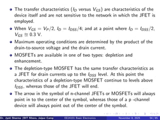
54.
The transfer characteristics(ID versus VGS ) are characteristics of the
device itself and are not sensitive to the network in which the JFET is
employed.
When VGS = VP/2, ID = IDSS /4; and at a point where ID = IDSS /2,
VGS ≊ 0.3 V.
Maximum operating conditions are determined by the product of the
drain-to-source voltage and the drain current.
MOSFETs are available in one of two types: depletion and
enhancement.
The depletion-type MOSFET has the same transfer characteristics as
a JFET for drain currents up to the IDSS level. At this point the
characteristics of a depletion-type MOSFET continue to levels above
IDSS , whereas those of the JFET will end.
The arrow in the symbol of n-channel JFETs or MOSFETs will always
point in to the center of the symbol, whereas those of a p -channel
device will always point out of the center of the symbol.
Dr. Jyoti Sharma (BIT Mesra, Jaipur Campus) EE24101 Basic Electronics November 8, 2025 54 / 85
55.
The transfer characteristicsof an enhancement-type MOSFET are not
defined by Shockley’s equation but rather by a nonlinear equation
controlled by the gate-to-source voltage, the threshold voltage, and a
constant k defined by the device employed. The resulting plot of ID
versus VGS rises exponentially with increasing values of VGS .
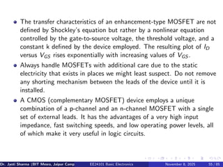
Always handle MOSFETs with additional care due to the static
electricity that exists in places we might least suspect. Do not remove
any shorting mechanism between the leads of the device until it is
installed.
A CMOS (complementary MOSFET) device employs a unique
combination of a p-channel and an n-channel MOSFET with a single
set of external leads. It has the advantages of a very high input
impedance, fast switching speeds, and low operating power levels, all
of which make it very useful in logic circuits.
Dr. Jyoti Sharma (BIT Mesra, Jaipur Campus) EE24101 Basic Electronics November 8, 2025 55 / 85
56.
CS biasing ofJFET and MOSFET
The biasing levels for a silicon transistor configuration can be
obtained using the characteristic equations VBE = 0.7 V, IC = βIB,
and IC = αIE.
The link between input and output variables is provided by β, which
is assumed to be fixed in magnitude for the analysis to be performed.
The fact that beta is a constant establishes a linear relationship
between IC and IB.
Doubling the value of IB will double the level of IC, and so on.
For the field-effect transistor, the relationship between input and
output quantities is nonlinear due to the squared term in Shockley’s
equation.
Linear relationships result in straight lines when plotted on a graph of
one variable versus the other, while nonlinear functions result in
curves as obtained for the transfer characteristics of a JFET.
Dr. Jyoti Sharma (BIT Mesra, Jaipur Campus) EE24101 Basic Electronics November 8, 2025 56 / 85
57.
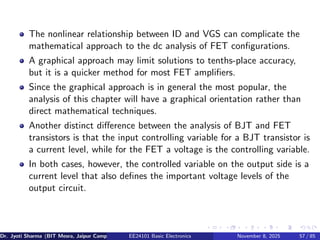
The nonlinear relationshipbetween ID and VGS can complicate the
mathematical approach to the dc analysis of FET configurations.
A graphical approach may limit solutions to tenths-place accuracy,
but it is a quicker method for most FET amplifiers.
Since the graphical approach is in general the most popular, the
analysis of this chapter will have a graphical orientation rather than
direct mathematical techniques.
Another distinct difference between the analysis of BJT and FET
transistors is that the input controlling variable for a BJT transistor is
a current level, while for the FET a voltage is the controlling variable.
In both cases, however, the controlled variable on the output side is a
current level that also defines the important voltage levels of the
output circuit.
Dr. Jyoti Sharma (BIT Mesra, Jaipur Campus) EE24101 Basic Electronics November 8, 2025 57 / 85
58.
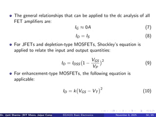
The general relationshipsthat can be applied to the dc analysis of all
FET amplifiers are:
IG ≈ 0A (7)
ID = IS (8)
For JFETs and depletion-type MOSFETs, Shockley’s equation is
applied to relate the input and output quantities:
ID = IDSS 1 −
VGS
VP
2
(9)
For enhancement-type MOSFETs, the following equation is
applicable:
ID = k VGS − VT
2
(10)
Dr. Jyoti Sharma (BIT Mesra, Jaipur Campus) EE24101 Basic Electronics November 8, 2025 58 / 85
59.
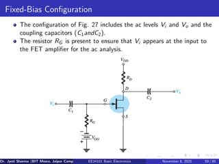
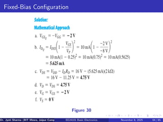
Fixed-Bias Configuration
The configurationof Fig. 27 includes the ac levels Vi and Vo and the
coupling capacitors (C1andC2).
The resistor RG is present to ensure that Vi appears at the input to
the FET amplifier for the ac analysis.
Dr. Jyoti Sharma (BIT Mesra, Jaipur Campus) EE24101 Basic Electronics November 8, 2025 59 / 85
60.
Fixed-Bias Configuration
For thedc analysis,
IG ≈ 0A (11)
VRG
= IG RG = (0A)RG = 0V (12)
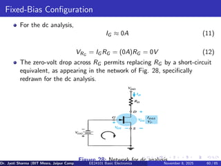
The zero-volt drop across RG permits replacing RG by a short-circuit
equivalent, as appearing in the network of Fig. 28, specifically
redrawn for the dc analysis.
Figure 28: Network for dc analysis.
Dr. Jyoti Sharma (BIT Mesra, Jaipur Campus) EE24101 Basic Electronics November 8, 2025 60 / 85
61.
Fixed-Bias Configuration
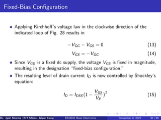
Applying Kirchhoff’svoltage law in the clockwise direction of the
indicated loop of Fig. 28 results in
−VGG − VGS = 0 (13)
VGS = −VGG (14)
Since VGG is a fixed dc supply, the voltage VGS is fixed in magnitude,
resulting in the designation “fixed-bias configuration.”
The resulting level of drain current ID is now controlled by Shockley’s
equation:
ID = IDSS 1 −
VGS
VP
2
(15)
Dr. Jyoti Sharma (BIT Mesra, Jaipur Campus) EE24101 Basic Electronics November 8, 2025 61 / 85
62.
Fixed-Bias Configuration
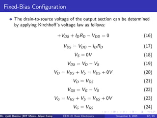
The drain-to-sourcevoltage of the output section can be determined
by applying Kirchhoff’s voltage law as follows:
+VDS + IDRD − VDD = 0 (16)
VDS = VDD − IDRD (17)
VS = 0V (18)
VDS = VD − VS (19)
VD = VDS + VS = VDS + 0V (20)
VD = VDS (21)
VGS = VG − VS (22)
VG = VGS + VS = VGS + 0V (23)
VG = VGS (24)
Dr. Jyoti Sharma (BIT Mesra, Jaipur Campus) EE24101 Basic Electronics November 8, 2025 62 / 85
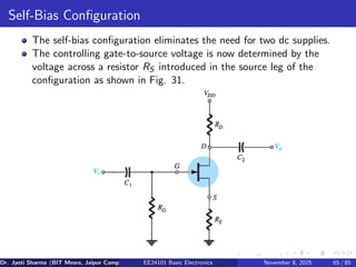
Self-Bias Configuration
The self-biasconfiguration eliminates the need for two dc supplies.
The controlling gate-to-source voltage is now determined by the
voltage across a resistor RS introduced in the source leg of the
configuration as shown in Fig. 31.
Dr. Jyoti Sharma (BIT Mesra, Jaipur Campus) EE24101 Basic Electronics November 8, 2025 65 / 85
66.
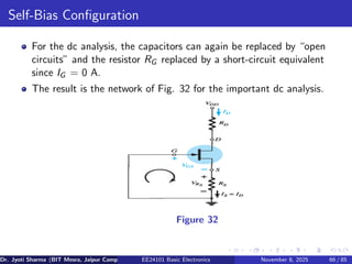
Self-Bias Configuration
For thedc analysis, the capacitors can again be replaced by “open
circuits” and the resistor RG replaced by a short-circuit equivalent
since IG = 0 A.
The result is the network of Fig. 32 for the important dc analysis.
Figure 32
Dr. Jyoti Sharma (BIT Mesra, Jaipur Campus) EE24101 Basic Electronics November 8, 2025 66 / 85
67.
Self-Bias Configuration
The currentthrough RS is the source current IS , but IS = ID and
VRS
= IDRS (25)
For the indicated closed loop of Fig. 32, we find that
−VGS − VRS
= 0 (26)
VGS = −VRS
(27)
VGS = −IDRS (28)
Note in this case that VGS is a function of the output current ID and
not fixed in magnitude as occurred for the fixed-bias configuration.
Dr. Jyoti Sharma (BIT Mesra, Jaipur Campus) EE24101 Basic Electronics November 8, 2025 67 / 85
68.
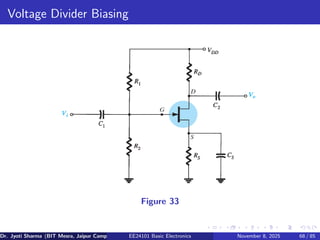
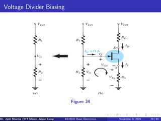
Voltage Divider Biasing
Figure33
Dr. Jyoti Sharma (BIT Mesra, Jaipur Campus) EE24101 Basic Electronics November 8, 2025 68 / 85
69.
The network ofFig. 33 is redrawn as shown in Fig. 34 for the dc
analysis.
Note that all the capacitors, including the bypass capacitor CS , have
been replaced by an ”open circuit” equivalent in Fig. 34b.
In addition, the source VDD was separated into two equivalent sources
to permit a further separation of the input and output regions of the
network.
Since IG = 0 A, Kirchhoff’s current law requires that IR1 = IR2, and
the series equivalent circuit appearing to the left of the figure can be
used to find the level of VG .
The voltage VG , equal to the voltage across R2, can be found using
the voltage-divider rule and Fig. 33a as follows:
VG =
R2VDD
R! + R2
(29)
Dr. Jyoti Sharma (BIT Mesra, Jaipur Campus) EE24101 Basic Electronics November 8, 2025 69 / 85
70.
Voltage Divider Biasing
Figure34
Dr. Jyoti Sharma (BIT Mesra, Jaipur Campus) EE24101 Basic Electronics November 8, 2025 70 / 85
71.
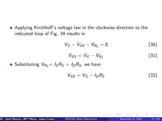
Applying Kirchhoff’s voltagelaw in the clockwise direction to the
indicated loop of Fig. 34 results in
VG − VGS − VRS
= 0 (30)
VGS = VG − VRS
(31)
Substituting VRS
= IS RS = IDRS , we have
VGS = VG − IDRS (32)
Dr. Jyoti Sharma (BIT Mesra, Jaipur Campus) EE24101 Basic Electronics November 8, 2025 71 / 85
72.
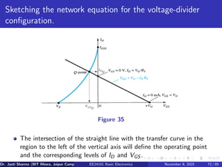
Sketching the networkequation for the voltage-divider
configuration.
Figure 35
The intersection of the straight line with the transfer curve in the
region to the left of the vertical axis will define the operating point
and the corresponding levels of ID and VGS .
Dr. Jyoti Sharma (BIT Mesra, Jaipur Campus) EE24101 Basic Electronics November 8, 2025 72 / 85
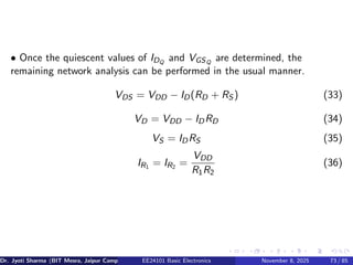
73.
• Once thequiescent values of IDQ
and VGSQ
are determined, the
remaining network analysis can be performed in the usual manner.
VDS = VDD − ID(RD + RS ) (33)
VD = VDD − IDRD (34)
VS = IDRS (35)
IR1 = IR2 =
VDD
R1R2
(36)
Dr. Jyoti Sharma (BIT Mesra, Jaipur Campus) EE24101 Basic Electronics November 8, 2025 73 / 85
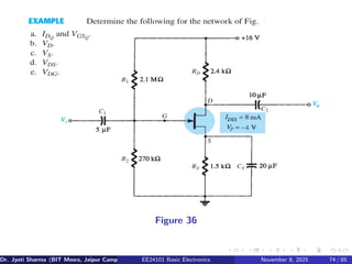
74.
Figure 36
Dr. JyotiSharma (BIT Mesra, Jaipur Campus) EE24101 Basic Electronics November 8, 2025 74 / 85
75.
Biasing of Depletion-TypeMOSFETs
The similarities in appearance between the transfer curves of JFETs
and depletion-type MOSFETs permit a similar analysis of each in the
dc domain.
The primary difference between the two is the fact that depletion-type
MOSFETs permit operating points with positive values of VGS and
levels of ID that exceed IDSS .
In fact, for all the configurations discussed thus far, the analysis is the
same if the JFET is replaced by a depletion-type MOSFET.
Dr. Jyoti Sharma (BIT Mesra, Jaipur Campus) EE24101 Basic Electronics November 8, 2025 75 / 85
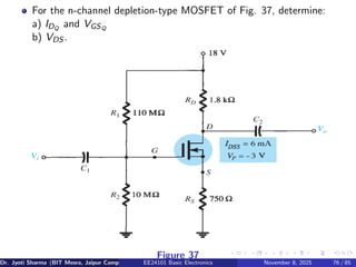
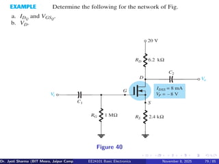
76.
For the n-channeldepletion-type MOSFET of Fig. 37, determine:
a) IDQ
and VGSQ
b) VDS .
Figure 37
Dr. Jyoti Sharma (BIT Mesra, Jaipur Campus) EE24101 Basic Electronics November 8, 2025 76 / 85
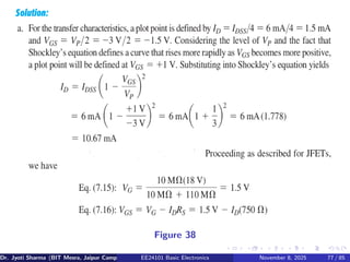
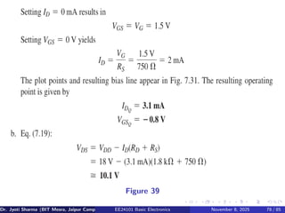
77.
Figure 38
Dr. JyotiSharma (BIT Mesra, Jaipur Campus) EE24101 Basic Electronics November 8, 2025 77 / 85
78.
Figure 39
Dr. JyotiSharma (BIT Mesra, Jaipur Campus) EE24101 Basic Electronics November 8, 2025 78 / 85
79.
Figure 40
Dr. JyotiSharma (BIT Mesra, Jaipur Campus) EE24101 Basic Electronics November 8, 2025 79 / 85
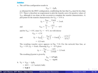
80.
Dr. Jyoti Sharma(BIT Mesra, Jaipur Campus) EE24101 Basic Electronics November 8, 2025 80 / 85
81.
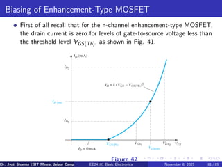
Biasing of Enhancement-TypeMOSFET
First of all recall that for the n-channel enhancement-type MOSFET,
the drain current is zero for levels of gate-to-source voltage less than
the threshold level VGS(Th), as shown in Fig. 41.
Figure 42
Dr. Jyoti Sharma (BIT Mesra, Jaipur Campus) EE24101 Basic Electronics November 8, 2025 81 / 85
82.
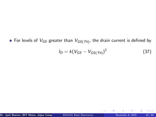
For levels ofVGS greater than VGS(Th), the drain current is defined by
ID = k(VGS − VGS(Th))2
(37)
Dr. Jyoti Sharma (BIT Mesra, Jaipur Campus) EE24101 Basic Electronics November 8, 2025 82 / 85
83.
Voltage Divider Biasof EMOSFET
Dr. Jyoti Sharma (BIT Mesra, Jaipur Campus) EE24101 Basic Electronics November 8, 2025 83 / 85
84.
PYQ
Define pinch-off voltagein JFET.
List out the advantages of the FET over conventional BJT?
Determine the relation between the drain resistance,
transconductance and amplification factor of FET.
With the help of neat sketches explain the construction and operation
of p-channel enhancement type MOSFET.
Explain the construction, operation and drain characteristics of
n-channel JFET.
What are the two main types of field effect transistor? What are the
advantages of the FET over a conventional transistor?
Give basic construction, symbol, characteristic curves for the
N-channel depletion type MOSFET and explain its operation.
Define pinch-off voltage for a JFET. Also explain the operation of
n-channel enhancement-type MOSFET with the help of neat sketches.
Dr. Jyoti Sharma (BIT Mesra, Jaipur Campus) EE24101 Basic Electronics November 8, 2025 84 / 85
85.
END OF MODULE3
Dr. Jyoti Sharma (BIT Mesra, Jaipur Campus) EE24101 Basic Electronics November 8, 2025 85 / 85


![Applying Kirchhoff’s voltage law to the terminal voltages of the
MOSFET of Fig. 22, we find that
VDG = VDS − VGS (3)
If VGS is held fixed at some value such as 8 V and VDS is increased
from 2 V to 5 V, the voltage VDG [by Eq. 3] will increase from -6 V
to -3 V and the gate will become less and less positive with respect to
the drain.
This reduction in gate-to-drain voltage will in turn reduce the
attractive forces for free carriers (electrons) in this region of the
induced channel, causing a reduction in the effective channel width.
Eventually, the channel will be reduced to the point of pinch-off and a
saturation condition will be established as described earlier for the
JFET and depletion-type MOSFET.
In other words, any further increase in VDS at the fixed value of VGS
will not affect the saturation level of ID until breakdown conditions
are encountered.
Dr. Jyoti Sharma (BIT Mesra, Jaipur Campus) EE24101 Basic Electronics November 8, 2025 45 / 85](https://image.slidesharecdn.com/ec24101bemodule3-251130025810-d16e7d41/85/EC24101-BE-Module-3-basic-electronic-by-birla-pdf-45-320.jpg)